Note: Descriptions are shown in the official language in which they were submitted.
CA 02526436 2005-12-06
Method and System for Programming and Driving
Active Matrix Light Emitting Device Pixel
FIELD OF INVENTION
[0001 ] The present invention relates to a light emitting device displays, and
more
specifically to a driving technique for the light emitting device displays.
BACKGROUND OF THE INVENTION
[0002] Recently active-matrix organic light-emitting diode (AMOLED) displays
with
amorphous silicon (a-Si), poly-silicon, organic, or other driving backplane
have
become more attractive due to advantages over active matrix liquid crystal
displays. An
AMOLED display using a-Si backplanes, for example, has the advantages which
include low temperature fabrication that broadens the use of different
substrates and
makes flexible displays feasible, and its low cost fabrication that yields
high resolution
displays with a wide viewing angle.
[0003] The AMOLED display includes an array of rows and columns of pixels,
each
having an organic light-emitting diode (OLED) and backplane electronics
arranged in
the array of rows and columns. Since the OLED is a current driven device, the
pixel
circuit of the AMOLED should be capable of providing an accurate and constant
drive
current.
[0004] Figure 1 shows a pixel circuit as disclosed in U.S. Patent. No.
5,748,160. The
pixel circuit of Figure 1 includes an OLED 10, a driving thin film transistor
(TFT) 11,
a switch TFT 13, and a storage capacitor 14. The drain terminal of the driving
TFT 11
is connected to the OLED 10. The gate terminal of the driving TFT 11 is
connected to
a column line 12 through the switch TFT 13. The storage capacitor 14, which is
connected between the gate terminal of the driving TFT 11 and the ground, is
used to
maintain the voltage at the gate terminal of the driving TFT 11 when the pixel
circuit is
disconnected from the column line 12. The current through the OLED 10 strongly
depends on the characteristic parameters of the driving TFT 11. Since the
characteristic
parameters of the driving TFT 11, in particular the threshold voltage under
bias stress,
vary by time, and such changes may differ from pixel to pixel, the induced
image
distortion may be unacceptably high.
CA 02526436 2005-12-06
[0005] U.S. Patent No. 6,229,508 discloses a voltage-programmed pixel circuit
which
provides, to an OLED, a current independent of the threshold voltage of a
driving TFT.
In this pixel, the gate-source voltage of the driving TFT is composed of a
programming
voltage and the threshold voltage of the driving TFT. A drawback of U.S.
Patent No.
6,229,508 is that the pixel circuit requires extra transistors, and is
complex, which
results in a reduced yield, reduced pixel aperture, and reduced lifetime for
the display.
[0006] Another method to make a pixel circuit less sensitive to a shift in the
threshold
voltage of the driving transistor is to use current programmed pixel circuits,
such as
pixel circuits disclosed in U.S. Patent No. 6,734,636. In the conventional
current
to programmed pixel circuits, the gate-source voltage of the driving TFT is
self adjusted
based on the current that flows through it in the next frame, so that the OLED
current is
less dependent on the current-voltage characteristics of the driving TFT. A
drawback
of the current-programmed pixel circuit is that an overhead associated with
low
programming current levels arises from the column line charging time due to
the large
15 line capacitance.
SUMMARY OF THE INVENTION
[0007] It is an object of the invention to provide a method and system that
obviates or
mitigates at least one of the disadvantages of existing systems.
[0008] In accordance with an aspect to the present invention there is provided
a method
20 of programming and driving a display system, the display system includes: a
display
array having a plurality of pixel circuits arranged in row and column, each
pixel circuit
having: a light emitting device having a first terminal and a second terminal,
the first
terminal of the lighting device being connected to a voltage supply electrode;
a
capacitor having a first terminal and a second terminal; a switch transistor
having a gate
2s terminal, a first terminal and a second terminal, the gate terminal of the
switch transistor
being connected to a select line, the first terminal of the switch transistor
being
connected to a signal line for transfernng voltage data, the second terminal
of the switch
transistor being connected to the first terminal of the capacitor; and a
driving transistor
having a gate terminal, a first terminal and a second terminal, the gate
terminal of the
3o driving transistor being connected to the second terminal of the switch
transistor and the
first terminal of the capacitor at a first node (A), the first terminal of the
driving
CA 02526436 2005-12-06
transistor being connected to the second terminal of the light emitting device
and the
second terminal of the capacitor at a second node (B), the second terminal of
the driving
transistor being connected to a controllable voltage supply line; a driver for
driving the
select line, the controllable voltage supply line and the signal line to
operate the display
array; the method including the steps o~ at a programming cycle, at a first
operating
cycle, charging the second node at a first voltage defined by (VREF-VT) or
(-VREF+VT), where VREF represents a reference voltage and VT represents a
threshold voltage of the driving transistor; at a second operating cycle,
charging the first
node at a second voltage defined by (VREF+VP) or (-VREF+VP) so that the
difference
between the first and second node voltages is stored in the storage capacitor,
where VP
represents a programming voltage; at a driving cycle, applying the voltage
stored in the
storage capacitor to the gate terminal of the driving transistor.
[0009] In accordance with a further aspect to the present invention there is
provided a
method of programming and driving a display system, the display system
includes: a
display array having a plurality of pixel circuits arranged in row and column,
each pixel
circuit having: a light emitting device having a first terminal and a second
terminal, the
first terminal of the lighting device being connected to a voltage supply
electrode; a first
capacitor and a second capacitor, each having a first terminal and a second
terminal; a
first switch transistor having a gate terminal, a first terminal and a second
terminal, the
gate terminal of the first switch transistor being connected to a first select
line, the first
terminal of the first switch transistor being connected to the second terminal
of the light
emitting device, the second terminal of the first switch being connected to
the first
terminal of the first capacitor; a second switch transistor having a gate
terminal, a first
terminal and a second terminal, the gate terminal of the second switch
transistor being
connected to a second select line, the first terminal of the second switch
transistor being
connected to a signal line for transfernng voltage data; a driving transistor
having a gate
terminal, a first terminal and a second terminal, the first terminal of the
driving
transistor being connected to the second terminal of the light emitting device
at a first
node (A), the gate terminal of the driving transistor being connected to the
second
terminal of the first switch transistor and the first terminal of the first
capacitor at a
second node (B), the second terminal of the driving transistor being connected
to a
controllable voltage supply line; the second terminal of the second switch
transistor
CA 02526436 2005-12-06
being connected to the second terminal of the first capacitor and the first
terminal of the
second capacitor at a third node (C); a driver for driving the first and
second select line,
the controllable voltage supply line and the signal line to operate the
display array, the
method including the steps of at a programming cycle, at a first operating
cycle,
controlling the voltage of each of the first node and the second node so as to
store
(VT+VP) or -(VT+VP) in the first storage capacitor, where VT represents a
threshold
voltage of the driving transistor, VP represents a programming voltage; at a
second
operating cycle, discharging the third node; at a driving cycle, applying the
voltage
stored in the storage capacitor to the gate terminal of the driving
transistor.
io [0010] In accordance with a further aspect to the present invention there
is provided a
display system including: a display array having a plurality of pixel circuits
arranged in
row and column, each pixel circuit having: a light emitting device having a
first
terminal and a second terminal, the first terminal of the lighting device
being connected
to a voltage supply electrode; a capacitor having a first terminal and a
second terminal;
15 a switch transistor having a gate terminal, a first terminal and a second
terminal, the
gate terminal of the switch transistor being connected to a select line, the
first terminal
of the switch transistor being connected to a signal line for transfernng
voltage data, the
second terminal of the switch transistor being connected to the first terminal
of the
capacitor; and a driving transistor having a gate terminal, a first terminal
and a second
2o terminal, the gate terminal of the driving transistor being connected to
the second
terminal of the switch transistor and the first terminal of the capacitor at a
first node (A),
the first terminal of the driving transistor being connected to the second
terminal of the
light emitting device and the second terminal of the capacitor at a second
node (B), the
second terminal of the driving transistor being connected to a controllable
voltage
25 supply line; a driver for driving the select line, the controllable voltage
supply line and
the signal line to operate the display array; and a controller for
implementing a
programming cycle and a driving cycle on each row of the display array using
the
driver; wherein the programming cycle includes a first operating cycle and a
second
operating cycle, wherein at the first operating cycle, the second node is
charged at a first
30 voltage defined by (VREF-VT) or (-VREF+VT), where VREF represents a
reference
voltage and VT represents a threshold voltage of the driving transistor, at
the second
operating cycle, the first node is charged at a second voltage defined by
(VREF+VP) or
CA 02526436 2005-12-06
(-VREF+VP) so that the difference between the first and second node voltages
is stored
in the storage capacitor, where VP represents a programming voltage; wherein
at the
driving cycle, the voltage stored in the storage capacitor is applied to the
gate terminal
of the driving transistor.
[0011] In accordance with a further aspect to the present invention there is
provided a
display system including: a display array having a plurality of pixel circuits
arranged in
row and column, each pixel circuit having: a light emitting device having a
first
terminal and a second terminal, the first terminal of the lighting device
being connected
to a voltage supply electrode; a first capacitor and a second capacitor, each
having a first
1o terminal and a second terminal; a first switch transistor having a gate
terminal, a first
terminal and a second terminal, the gate terminal of the first switch
transistor being
connected to a first select line, the first terminal of the first switch
transistor being
connected to the second terminal of the light emitting device, the second
terminal of the
first switch being connected to the first terminal of the first capacitor; a
second switch
15 transistor having a gate terminal, a first terminal and a second terminal,
the gate
terminal of the second switch transistor being connected to a second select
line, the first
terminal of the second switch transistor being connected to a signal line for
transferring
voltage data; a driving transistor having a gate terminal, a first terminal
and a second
terminal, the first terminal of the driving transistor being connected to the
second
2o terminal of the light emitting device at a first node (A), the gate
terminal of the driving
transistor being connected to the second terminal of the first switch
transistor and the
first terminal of the first capacitor at a second node (B), the second
terminal of the
driving transistor being connected to a controllable voltage supply line; the
second
terminal of the second switch transistor being connected to the second
terminal of the
z5 first capacitor and the first terminal of the second capacitor at a third
node (C); a driver
for driving the first and second select line, the controllable voltage supply
line and the
signal line to operate the display array; and a controller for implementing a
programming cycle and a driving cycle on each row of the display array using
the
driver; wherein the programming cycle includes a first operating cycle and a
second
30 operating cycle, wherein at the first operating cycle, the voltage of each
of the first node
and the second node is controlled so as to store (VT+VP) or -(VT+VP) in the
first
storage capacitor, where VT represents a threshold voltage of the driving
transistor, VP
CA 02526436 2005-12-06
represents a programming voltage, at the second operating cycle, the third
node is
discharged, wherein at the driving cycle, the voltage stored in the storage
capacitor is
applied to the gate terminal of the driving transistor.
[0012] This summary of the invention does not necessarily describe all
features of the
invention.
[0013] Other aspects and features of the present invention will be readily
apparent to
those skilled in the art from a review of the following detailed description
of preferred
embodiments in conjunction with the accompanying drawings.
BRIEF DESCRIPTION OF THE DRAWINGS
[0014] These and other features of the invention will become more apparent
from the
following description in which reference is made to the appended drawings
wherein:
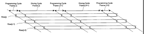
[001 S] Figure 1 is a diagram showing a conventional 2-TFT voltage programmed
pixel
circuit;
[0016] Figure 2 is a timing diagram showing an example of programming and
driving
cycles in accordance with an embodiment of the present invention, which is
applied to
a display array;
[0017] Figure 3 is a diagram showing a pixel circuit to which programming and
driving
technique in accordance with an embodiment of the present invention is
applied;
[0018] Figure 4 is a timing diagram showing an example of waveforms for
programming and driving the pixel circuit of Figure 3;
[0019] Figure 5 is a diagram showing a lifetime test result for the pixel
circuit of Figure
3;
[0020] Figure 6 is a diagram showing a display system having the pixel circuit
of Figure
3;
z5 [0021] Figure 7(a) is a diagram showing an example of the array structure
having top
emission pixels which are applicable to the array of Figure 6;
6
CA 02526436 2005-12-06
[0022] Figure 7(b) is a diagram showing an example of the array structure
having
bottom emission pixels which are applicable to the array of Figure 6;
[0023] Figure 8 is a diagram showing a pixel circuit to which programming and
driving
technique in accordance with a further embodiment of the present invention is
applied;
[0024] Figure 9 is a timing diagram showing an example of waveforms for
programming and driving the pixel circuit of Figure 8;
[0025] Figure 10 is a diagram showing a pixel circuit to which programming and
driving technique in accordance with a further embodiment of the present
invention is
applied;
to [0026] Figure 11 is a timing diagram showing an example of waveforms for
programming and driving the pixel circuit of Figure 10;
[0027] Figure 12 is a diagram showing a pixel circuit to which programming and
driving technique in accordance with a further embodiment of the present
invention is
applied;
15 [0028] Figure 13 is a timing diagram showing an example of waveforms for
programming and driving the pixel circuit of Figure 12;
[0029] Figure 14 is a diagram showing a pixel circuit to which programming and
driving technique in accordance with a further embodiment of the present
invention is
applied;
20 [0030] Figure 15 is a timing diagram showing an example of waveforms for
programming and driving the pixel circuit of Figure 14;
[0031 ] Figure 16 is a diagram showing a display system having the pixel
circuit of
Figure 14;
[0032] Figure 17 is a diagram showing a pixel circuit to which programming and
25 driving technique in accordance with a further embodiment of the present
invention is
applied;
CA 02526436 2005-12-06
[0033] Figure 18 is a timing diagram showing an example of waveforms for
programming and driving the pixel circuit of Figure 17;
[0034] Figure 19 is a diagram showing a pixel circuit to which programming and
driving technique in accordance with a further embodiment of the present
invention is
applied;
[0035] Figure 20 is a timing diagram showing an example of waveforms for
programming and driving the pixel circuit of Figure 19;
[0036] Figure 21 is a diagram showing a pixel circuit to which programming and
driving technique in accordance with a further embodiment of the present
invention is
to applied; and
[0037] Figure 22 is a timing diagram showing an example of waveforms for
programming and driving the pixel circuit of Figure 21;
DETAILED DESCRIPTION OF THE PREFERRED EMBODIMENTS OF THE
INVENTION
15 [0038] Embodiments of the present invention are described using a pixel
having an
organic light emitting diode (OLED) and a driving thin film transistor (TFT).
However,
the pixel may include any light emitting device other than OLED, and the pixel
may
include any driving transistor other than TFT. It is noted that in the
description, "pixel
circuit" and "pixel" may be used interchangeably.
2o [0039] Figure 2 is a diagram showing programming and driving cycles in
accordance
with an embodiment of the present invention. In Figure 2, each of ROW(j),
ROW(j+1 ),
and ROW(j+2) represents a row of the display array where a plurality of pixel
circuits
are arranged in row and column.
[0040] The programming and driving cycle for a frame occurs after the
programming
25 and driving cycle for a next frame. The programming and driving cycles for
the frame
at a ROW overlaps with the programming and driving cycles for the same frame
at a
next ROW. As described below, during the programming cycle, the time depending
parameters) of the pixel circuit is extracted to generate a stable pixel
current.
CA 02526436 2005-12-06
[0041 ] Figure 3 illustrates a pixel circuit 200 to which programming and
driving
technique in accordance with an embodiment of the present invention is
applied. The
pixel circuit 200 includes an OLED 20, a storage capacitor 21, a driving
transistor 24,
and a switch transistor 26. The pixel circuit 200 is a voltage programmed
pixel circuit.
Each of the transistors 24 and 26 has a gate terminal, a first terminal and a
second
terminal. In the description, the first terminal (second terminal) may be, but
not limited
to, a drain terminal or a source terminal (a source terminal or a drain
terminal).
[0042] The transistors 24 and 26 are n-type TFTs. However, the transistors 24
and 26
may be p-type transistors. As described below, the driving technique applied
to the
1o pixel circuit 200 is also applicable to a complementary pixel circuit
having p-type
transistors as shown in Figure 14. The transistors 24 and 26 may be fabricated
using
amorphous silicon, nano/micxo crystalline silicon, poly silicon, organic
semiconductors
technologies (e.g. organic TFT), NMOS/PMOS technology or CMOS technology (e.g.
MOSFET).
15 [0043] The first terminal of the driving transistor 24 is connected to a
controllable
voltage supply line VDD. The second terminal of the driving transistor 24 is
connected
to the anode electrode of the OLED 20. The gate terminal of the driving
transistor 24 is
connected to a signal line VDATA through the switch transistor 26. The storage
capacitor 21 is connected between the source and gate terminals of the driving
transistor
20 24.
[0044] The gate terminal of the switch transistor 26 is connected to a select
line SEL.
The first terminal of the switch transistor 26 is connected to the signal line
VDATA.
The second terminal of the switch transistor 26 is connected to the gate
terminal of the
driving transistor 24. The cathode electrode of the OLED 20 is connected to a
ground
25 voltage supply electrode.
[0045] The transistors 24 and 26 and the storage capacitor 21 are connected at
node A1.
The transistor 24, the OLED 20 and the storage capacitor 21 are connected at
node B 1.
[0046] Figure 4 illustrates a timing diagram showing an example of waveforms
for
programming and driving the pixel circuit 200 of Figure 3. Refernng to Figures
3 and
30 4, the operation of the pixel circuit 200 includes a programming cycle
having three
9
CA 02526436 2005-12-06
d
operating cycles X11, X12 and X13, and a driving cycle having one operating
cycle
X14.
[0047] During the programming cycle, node B 1 is charged to the negative
threshold
voltage of the driving transistor 24, and node A1 is charged to a programming
voltage
VP.
[0048] As a result, the gate-source voltage of the driving transistor 24 goes
to:
VGS=VP-(-VT)=VP+VT ...(1)
where VGS represents the gate-source voltage of the driving transistor 24, and
VT
represents the threshold voltage of the driving transistor 24.
[0049] Since the driving transistor 24 is in saturation regime of operation,
its current is
defined mainly by its gate-source voltage. As a result the current of the
driving
transistor 24 remains constant even if the OLED voltage changes, since its
gate-source
voltage is stored in the storage capacitor 21.
[0050] In the first operating cycle X11: VDD goes to a compensating voltage
VCOMPB, and VDATA goes to a high positive compensating voltage VCOMPA, and
SEL is high. As a result, node A1 is charged to VCOMPA and node Bl is charged
to
VCOMPB.
[0051] In the second operating cycle X12: While VDATA goes to a reference
voltage
VREF, node B1 is discharged through the driving transistor 24 until the
driving
2o transistor 24 turns off. As a result, the voltage of node B1 reaches (VREF-
VT). VDD
has a positive voltage VH to increase the speed of this cycle X12. For optimal
setting
time, VH can be set to be equal to the operating voltage which is the voltage
on VDD
during the driving cycle.
[0052] In the third operating cycle X13: VDD goes to its operating voltage.
While SEL
is high, node A1 is charged to (VP+VREF). Because the capacitance 22 of the
OLED
20 is large, the voltage at node B1 stays at the voltage generated in the
previous cycle
X12. Thus, the voltage of node B 1 is (VREF-VT). Therefore, the gate-source
voltage
io
CA 02526436 2005-12-06
of the driving transistor 24 is (VP+VT), and this gate-source voltage is
stored in the
storage capacitor 21.
[0053] In the fourth operating cycle X14: SEL and VDATA go to zero. VDD is the
same as that of the third operating cycle X13. However, VDD may be higher than
that
of the third operating cycle X13. The voltage stored in the storage capacitor
21 is
applied to the gate terminal of the driving transistor 24. Since the gate-
source voltage
of the driving transistor 24 include its threshold voltage and also is
independent of the
OLED voltage, the degradation of the OLED 20 and instability of the driving
transistor
24 does not affect the amount of current flowing through the driving
transistor 24 and
1 o the OLED 20.
[0054] It is noted that the pixel circuit 200 can be operated with different
values of
VCOMPB, VCOMPA, VP, VREF and VH. VCOMPB, VCOMPA, VP, VREF and VH
define the lifetime of the pixel circuit 200. Thus, these voltages can be
defined in
accordance with the pixel specifications.
[0055] Figure 5 illustrates a lifetime test result for the pixel circuit and
waveform
shown in Figures 3 and 4. In the test, a fabricated pixel circuit was put
under the
operation for a long time while the current of the driving transistor (24 of
Figure 3) was
monitored to investigate the stability of the driving scheme. The result shows
that
OLED current is stable after 120-hour operation. The VT shift of the driving
transistor
2o is 0.7 V.
[0056] Figure 6 illustrates a display system having the pixel circuit 200 of
Figure 3.
VDD1 and VDD2 of Figure 6 correspond to VDD of Figure 3. SEL1 and SEL2 of
Figure 6 correspond to SEL of Figure 3. VDATAl and VDATA2 of Figure 6
correspond to VDATA of Figure 3. The array of Figure 6 is an active matrix
light
emitting diode (AMOLED) display having a plurality of the pixel circuits 200
of Figure
3. The pixel circuits are arranged in rows and columns, and interconnections
41, 42 and
43 (VDATA1, SELL, VDD1). VDATA1 (or VDATA 2) is shared between the
common column pixels while SEL1 (or SEL2) and VDD1 (or VDD2) are shared
between common row pixels in the array structure.
11
CA 02526436 2005-12-06
[0057] A driver 300 is provided for driving VDATA1 and VDATA2. A driver 302 is
provided for driving VDD1, VDD2, SEL1 and SEL 2, however, the driver for VDD
and
SEL lines can also be implemented separately. A controller 304 controls the
drivers
300 and 302 to programming and driving the pixel circuits as described above.
The
timing diagram for programming and driving the display array of Figure 6 is as
shown
in Figure 2. Each programming and driving cycle may be the same as that of
Figure 4.
[0058] Figure 7(a) illustrates an example of array structure having top
emission pixels
are arranged. Figure 7(b) illustrates an example of array structure having
bottom
emission pixels are arranged. The array of Figure 6 may have array structure
shown in
1o Figure 7(a) or 7(b). In Figure 7(a), 400 represents a substrate, 402
represents a pixel
contact, 403 represents a (top emission) pixel circuit, and 404 represents a
transparent
top electrode on the OLEDs. In Figure 7(b), 410 represents a transparent
substrate, 411
represents a (bottom emission) pixel circuit, and 412 represents a top
electrode. All of
the pixel circuits including the TFTs, the storage capacitor, the SEL, VDATA,
and
15 VDD lines are fabricated together. After that, the OLEDs are fabricated for
all pixel
circuits. The OLED is connected to the corresponding driving transistor using
a via
(e.g. B 1 of Figure 3) as shown in Figures 7(a) and 7(b). The panel is
finished by
deposition of the top electrode on the OLEDs which can be a continuous layer,
reducing
the complexity of the design and can be used to turn the entire display ON/OFF
or
2o control the brightness.
[0059] Figure 8 illustrates a pixel circuit 202 to which programming and
driving
technique in accordance with a further embodiment of the present invention is
applied.
The pixel circuit 202 includes an OLED 50, two storage capacitors 52 and 53, a
driving
transistor 54, and switch transistors 56 and 58. The pixel circuit 202 is a
top emission,
25 voltage programmed pixel circuit. This embodiment principally works in the
same
manner as that of Figure 3. However, in the pixel circuit 202, the OLED 50 is
connected to the drain terminal of the driving transistor 54. As a result, the
circuit can
be connected to the cathode of the OLED 50. Thus, the OLED deposition can be
started
with the cathode.
30 [0060] The transistors 54, 56 and 58 are n-type TFTs. However, the
transistors 54, 56
and 58 may be p-type transistors The driving technique applied to the pixel
circuit 202
12
CA 02526436 2005-12-06
is also applicable to a complementary pixel circuit having p-type transistors
as shown in
Figure 17. The transistors 54, 56 and 58 may be fabricated using amorphous
silicon,
nano/micro crystalline silicon, poly silicon, organic semiconductors
technologies (e.g.
organic TFT), NMOS/PMOS technology or CMOS technology (e.g. MOSFET).
[0061 ] The first terminal of the driving transistor 54 is connected to the
cathode
electrode of the OLED 50. The second terminal of the driving transistor 54 is
connected
to a controllable voltage supply line VSS. The gate terminal of the driving
transistor 54
is connected to its first line (terminal) through the switch transistor 56.
The storage
capacitors 52 and 53 are in series, and are connected between the gate
terminal of the
to driving transistor 54 and a common ground. The voltage on the voltage
supply line
VSS is controllable. The common ground may be connected to VSS.
[0062] The gate terminal of the switch transistor 56 is connected to a first
select line
SELL. The first terminal of the switch transistor 56 is connected to the drain
terminal
of the driving transistor 54. The second terminal of the switch transistor 56
is
15 connected to the gate terminal of the driving transistor 54.
[0063] The gate terminal of the switch transistor 58 is connected to a second
select line
SEL2. The first terminal of the switch transistor 58 is connected to a signal
line
VDATA. The second terminal of the switch transistor 58 is connected to the
shared
terminal of the storage capacitors 52 and 53 (i.e. node C2). The anode
electrode of the
2o OLED 50 is connected to a voltage supply electrode VDD.
[0064] The OLED 50 and the transistors 54 and 56 are connected at node A2. The
storage capacitor 52 and the transistors 54 and 56 are connected at node B2.
[0065] Figure 9 illustrates a timing diagram showing an example of waveforms
for
programming and driving the pixel circuit 202 of Figure 8. Refernng to Figures
8 and
25 9, the operation of the pixel circuit 202 includes a programming cycle
having four
operating cycles X21, X22, X23 and X24, and a driving cycle having one
operating
cycle X25.
[0066] During the programming cycle, a programming voltage plus the threshold
voltage of the driving transistor 54 is stored in the storage capacitor 52.
The source
13
CA 02526436 2005-12-06
terminal of the driving transistor 54 goes to zero, and the second storage
capacitor 53 is
charged to zero.
[0067] As a result, the gate-source voltage of the driving transistor 54 goes
to:
VGS=VP+VT ...(2)
where VGS represents the gate-source voltage of the driving transistor 54, VP
represents the programming voltage, and VT represents the threshold voltage of
the
driving transistor 54.
[0068] In the first operating cycle X21: VSS goes to a high positive voltage,
and
VDATA is zero. SEL1 and SEL2 are high. Therefore, nodes AZ and B2 are charged
to
l0 a positive voltage.
[0069] In the second operating cycle X22: While SEL1 is low and the switch
transistor
56 is off, VDATA goes to a high positive voltage. As a result, the voltage at
node BZ
increases (i.e. bootstrapping) and node A2 is charged to the voltage of VSS.
At this
voltage, the OLED 50 is off.
[0070] In the third operating cycle X23: VSS goes to a reference voltage VREF.
VDATA goes to (VREF-VP). At the beginning of this cycle, the voltage of node
B2
becomes almost equal to the voltage of node A2 because the capacitance 51 of
the
OLED 50 is bigger than that of the storage capacitor 52. After that, the
voltage of node
B2 and the voltage of node AZ are discharged through the driving transistor 54
until the
driving transistor 54 turns off. As a result, the gate-source voltage of the
driving
transistor 54 is (VREF+VT), and the voltage stored in storage capacitor 52 is
(VP+VT).
[0071] In the fourth operating cycle X24: SEL1 is low. Since SEL2 is high, and
VDATA is zero, the voltage at node C2 goes to zero.
[0072] In the fifth operating cycle X25: VSS goes to its operating voltage
during the
driving cycle. In Figure 5, the operating voltage of VSS is zero. However, it
may be
any voltage other than zero. SEL2 is low. The voltage stored in the storage
capacitor
52 is applied to the gate terminal of the driving transistor 54. Accordingly,
a current
independent of the threshold voltage VT of the driving transistor 54 and the
voltage of
14
CA 02526436 2005-12-06
the OLED 50 flows through the driving transistor 54 and the OLED 50. Thus, the
degradation of the OLED 50 and instability of the driving transistor 54 does
not affect
the amount of the current flowing through the driving transistor 54 and the
OLED 50.
[0073] Figure 10 illustrates a pixel circuit 204 to which programming and
driving
technique in accordance with a further embodiment of the present invention is
applied.
The pixel circuit 204 includes an OLED 60, two storage capacitors 62 and 63, a
driving
transistor 64, and switch transistors 66 and 68. The pixel circuit 204 is a
top emission,
voltage programmed pixel circuit. The pixel circuit 204 principally works
similar to
that of in Figure 8. However, one common select line is used to operate the
pixel circuit
l0 204, which can increase the available pixel area and aperture ratio.
[0074] The transistors 64, 66 and 68 are n-type TFTs. However, The transistors
64, 66
and 68 may be p-type transistors. The driving technique applied to the pixel
circuit 204
is also applicable to a complementary pixel circuit having p-type transistors
as shown in
Figure 19. The transistors 64, 66 and 68 may be fabricated using amorphous
silicon,
15 nano/micro crystalline silicon, poly silicon, organic semiconductors
technologies (e.g.
organic TFT), NMOS/PMOS technology or CMOS technology (e.g. MOSFET).
[0075] The first terminal of the driving transistor 64 is connected to the
cathode
electrode of the OLED 60. The second terminal of the driving transistor 64 is
connected
to a controllable voltage supply line VSS. The gate terminal of the driving
transistor
2o 64 is connected to its first line (terminal) through the switch transistor
66. The storage
capacitors 62 and 63 are in series, and are connected between the gate
terminal of the
driving transistor 64 and the common ground. The voltage of the voltage supply
line
VSS is controllable. The common ground may be connected to VSS.
[0076] The gate terminal of the switch transistor 66 is connected to a select
line SEL.
25 The first terminal of the switch transistor 66 is connected to the first
terminal of the
driving transistor 64. The second terminal of the switch transistor 66 is
connected to the
gate terminal of the driving transistor 64.
[0077] The gate terminal of the switch transistor 68 is connected to the
select line SEL.
The first terminal of the switch transistor 68 is connected to a signal line
VDATA. The
3o second terminal is connected to the shared terminal of storage capacitors
62 and 63 (i.e.
r5
CA 02526436 2005-12-06
node C3). The anode electrode of the OLED 60 is connected to a voltage supply
electrode VDD.
[0078] The OLED 60 and the transistors 64 and 66 are connected at node A3. The
storage capacitor 62 and the transistors 64 and 66 are connected at node B3.
[0079] Figure 11 illustrates a timing diagram showing an example of waveforms
for
programming and driving the pixel circuit 204 of Figure 10. Referring to
Figures 10
and 11, the operation of the pixel circuit 204 includes a programming cycle
having three
operating cycles X31, X32 and X33, and a driving cycle includes one operating
cycle
X34.
[0080] During the programming cycle, a programming voltage plus the threshold
voltage of the driving transistor 64 is stored in the storage capacitor 62.
The source
terminal of the driving transistor 64 goes to zero and the storage capacitor
63 is charged
to zero.
[0081 ] As a result, the gate-source voltage of the driving transistor 64 goes
to:
VGS=VP+VT ...(3)
where VGS represents the gate-source voltage of the driving transistor 64, VP
represents the programming voltage, and VT represents the threshold voltage of
the
driving transistor 64.
[0082] In the first operating cycle X31: VSS goes to a high positive voltage,
and
2o VDATA is zero. SEL is high. As a result, nodes A3 and B3 are charged to a
positive
voltage. The OLED 60 turns off.
[0083] In the second operating cycle X32: While SEL is high, VSS goes to a
reference
voltage VREF. VDATA goes to (VREF-VP). As a result, the voltage at node B3 and
the voltage of node A3 are discharged through the driving transistor 64 until
the driving
transistor 64 turns off. The voltage of node B3 is (VREF+VT), and the voltage
stored
in the storage capacitor 62 is (VP+VT).
[0084] In the third operating cycle X33: SEL goes to VM. VM is an intermediate
voltage in which the switch transistor 66 is off and the switch transistor 68
is on.
16
CA 02526436 2005-12-06
VDATA goes to zero. Since SEL is VM and VDATA is zero, the voltage of node C3
goes to zero.
[0085] VM is defined as
VT3 «VM<VREF + VT1+VT2 ...(a)
where VT 1 represents the threshold voltage of the driving transistor 64, VT2
represents
the threshold voltage of the switch transistor 66, and VT3 represents the
threshold
voltage of the switch transistor 68.
[0086] The condition (a) forces the switch transistor 66 to be off and the
switch
transistor 68 to be on. The voltage stored in the storage capacitor 62 remains
intact.
to [0087] In the fourth operating cycle X34: VSS goes to its operating voltage
during the
driving cycle. In Figure 11, the operating voltage of VSS is zero. However,
the
operating voltage of VSS may be any voltage other than zero. SEL is low. The
voltage
stored in the storage capacitor 62 is applied to the gate of the driving
transistor 64. The
driving transistor 64 is ON. Accordingly, a current independent of the
threshold voltage
VT of the driving transistor 64 and the voltage of the OLED 60 flows through
the
driving transistor 64 and the OLED 60. Thus, the degradation of the OLED 60
and
instability of the driving transistor 64 does not affect the amount of the
current flowing
through the driving transistor 64 and the OLED 60.
[0088] Figure 12 illustrates a pixel circuit 206 to which programming and
driving
2o technique in accordance with a further embodiment of the present invention
is applied.
The pixel circuit 206 includes an OLED 70, two storage capacitors 72 and 73, a
driving
transistor 74, and switch transistors 76 and 78. The pixel circuit 206 is a
top emission,
voltage programmed pixel circuit.
[0089] The transistors 74, 76 and 78 are n-type TFTs. However, the transistors
74, 76
and 78 may be p-type transistors. The driving technique applied to the pixel
circuit 206
is also applicable to a complementary pixel circuit having p-type transistors
as shown in
Figure 21. The transistors 74, 76 and 78 may be fabricated using amorphous
silicon,
nano/micro crystalline silicon, poly silicon, organic semiconductors
technologies (e.g.
organic TFT), NMOS/PMOS technology or CMOS technology (e.g. MOSFET).
17
CA 02526436 2005-12-06
[0090] The first terminal of the driving transistor 74 is connected to the
cathode
electrode of the OLED 70. The second terminal of the driving transistor 74 is
connected
to a common ground. The gate terminal of the driving transistor 74 is
connected to its
first line (terminal) through the switch transistor 76. The storage capacitors
72 and 73
are in series, and are connected between the gate terminal of the driving
transistor 74
and the common ground.
[0091] The gate terminal of the switch transistor 76 is connected to a select
line SEL.
The first terminal of the switch transistor 76 is connected to the first
terminal of the
driving transistor 74. The second terminal of the switch transistor 76 is
connected to the
1o gate terminal of the driving transistor 74.
[0092] The gate terminal of the switch transistor 78 is connected to the
select line SEL.
The first terminal of the switch transistor 78 is connected to a signal line
VDATA. The
second terminal is connected to the shared terminal of storage capacitors 72
and 73 (i.e.
node C4). The anode electrode of the OLED 70 is connected to a voltage supply
15 electrode VDD. The voltage of the voltage electrode VDD is controllable.
[0093] The OLED 70 and the transistors 74 and 76 are connected at node A4. The
storage capacitor 72 and the transistors 74 and 76 are connected at node B4.
[0094] Figure 13 illustrates a timing diagram showing an example of waveforms
for
programming and driving the pixel circuit 206 of Figure 12. Refernng to
Figures 12
2o and 13, the operation of the pixel circuit 206 includes a programming cycle
having four
operating cycles X41, X42, X43 and X44, and a driving cycle having one driving
cycle
45.
[0095] During the programming cycle, a programming voltage plus the threshold
voltage of the driving transistor 74 is stored in the storage capacitor 72.
The source
25 terminal of the driving transistor 74 goes to zero and the storage
capacitor 73 is charged
to zero.
[0096] As a result, the gate-source voltage of the driving transistor 74 goes
to:
VGS=VP+VT ...(4)
CA 02526436 2005-12-06
where VGS represents the gate-source voltage of the driving transistor 74, VP
represents the programming voltage, and VT represents the threshold voltage of
the
driving transistor 74.
[0097] In the first operating cycle X41: SEL is high. VDATA goes to a low
voltage.
While VDD is high, node B4 and node A4 are charged to a positive voltage.
[0098] In the second operating cycle X42: SEL is low, and VDD goes to a
reference
voltage VREF where the OLED 70 is off.
[0099] In the third operating cycle X43: VDATA goes to (VREF2-VP) where VREF2
is a reference voltage. It is assumed that VREF2 is zero. However, VREF2 can
be any
to voltage other than zero. SEL is high. Therefore, the voltage of node B4 and
the voltage
of node A4 become equal at the beginning of this cycle. It is noted that the
first storage
capacitor 72 is large enough so that its voltage becomes dominant. After that,
node B4
is discharged through the driving transistor 74 until the driving transistor
74 turns off.
[00100] As a result, the voltage of node B4 is VT (i.e. the threshold voltage
of
the driving transistor 74). The voltage stored in the first storage capacitor
72 is
(VP-VREF2+VT)=(VP+VT) where VREF2=0.
[00101 ] In the fourth operating cycle X44: SEL goes to VM where VM is an
intermediate voltage at which the switch transistor 76 is off and the switch
transistor 78
is on. VM satisfies the following condition:
2o VT3 «VM< VP+VT . . . (b)
where VT3 represents the threshold voltage of the switch transistor 78.
[00102] VDATA goes to VREFZ (=0). The voltage of node C4 goes to VREF2
(=0).
[00103] This results in that the gate-source voltage VGS of the driving
transistor
74 is (VP+VT). Since VM<VP+VT, the switch transistor 76 is off, and the
voltage
stored in the storage capacitor 72 stays at VP+VT.
19
CA 02526436 2005-12-06
,r.
[00104] In the fifth operating cycle X45: VDD goes to the operating voltage.
SEL is low. The voltage stored in the storage capacitor 72 is applied to the
gate of the
driving transistor 74. Accordingly, a current independent of the threshold
voltage VT
of the driving transistor 74 and the voltage of the OLED 70 flows through the
driving
transistor 74 and the OLED 70. Thus, the degradation of the OLED 70 and
instability
of the driving transistor 74 does not affect the amount of the current flowing
through the
driving transistor 74 and the OLED 70.
[00105] Figure 14 illustrates a pixel circuit 208 to which programming and
driving technique in accordance with a further embodiment of the present
invention is
to applied. The pixel circuit 208 includes an OLED 80; a storage capacitor 81,
a driving
transistor 84 and a switch transistor 86. The pixel circuit 208 corresponds to
the pixel
circuit 200 of Figure 3, and a voltage programmed pixel circuit.
[00106] The transistors 84 and 86 are p-type TFTs. The transistors 84 and 86
may be fabricated using amorphous silicon, nano/micro crystalline silicon,
poly silicon,
organic semiconductors technologies (e.g. organic TFT), CMOS technology (e.g.
MOSFET) and any other technology which provides p-type transistors.
[00107] The first terminal of the driving transistor 84 is connected to a
controllable voltage supply line VSS. The second terminal of the driving
transistor 84
is connected to the cathode electrode of the OLED 80. The gate terminal of the
driving
2o transistor 84 is connected to a signal line VDATA through the switch
transistor 86. The
storage capacitor 81 is connected between the second terminal and the gate
terminal of
the driving transistor 84.
[00108] The gate terminal of the switch transistor 86 is connected to a select
line
SEL. The first terminal of the switch transistor 86 is connected to the signal
line
VDATA. The second terminal of the switch transistor 86 is connected to the
gate
terminal of the driving transistor 84. The anode electrode of the OLED 80 is
connected
to a ground voltage supply electrode.
[00109] The storage capacitor 81 and the transistors 84 and 85 are connected
at
node AS. The OLED 80, the storage capacitor 81 and the driving transistor 84
are
3o connected at node B5.
CA 02526436 2005-12-06
[00110] Figure 15 illustrates a timing diagram showing an example of
waveforms for programming and driving the pixel circuit 208 of Figure. Figure
15
corresponds to Figure 4. VDATA and VSS are used to programming and
compensating
for a time dependent parameter of the pixel circuit 208, which are similar to
VDATA
and VDD of Figure 4. Refernng to Figures 14 and 15, the operation of the pixel
circuit
208 includes a programming cycle having three operating cycles X51, X52 and
X53,
and a driving cycle having one operating cycle X54.
[00111] During the programming cycle, node BS is charged to a positive
threshold voltage of the driving transistor 84, and node A5 is charged to a
negative
programming voltage.
[00112] As a result, the gate-source voltage of the driving transistor 84 goes
to:
VGS=-VP+(-~VT~)=-VP-~VT~ ...(5)
where VGS represents the gate-source voltage of the driving transistor 84, VP
represents the programming voltage, and VT represents the threshold voltage of
the
driving transistor 84.
[00113] In the first operating cycle X51: VSS goes to a positive compensating
voltage VCOMPB, and VDATA goes to a negative compensating voltage
(-VCOMPA), and SEL is low. As a result, the switch transistor 86 is on. Node
AS is
charged to (-VCOMPA). Node B5 is charged to VCOMPB.
[00114] In the second operating cycle X52: VDATA goes to a reference voltage
VREF. Node B5 is discharged through the driving transistor 84 until the
driving
transistor 84 turns off. As a result, the voltage of node BS reaches
VREF+~VT~. VSS
goes to a negative voltage VL to increase the speed of this cycle X52. For the
optimal
setting time, VL is selected to be equal to the operating voltage which is the
voltage of
VSS during the driving cycle.
[00115] In the third operating cycle X53: While VSS is in the VL level, and
SEL
is low, node AS is charged to (VREF-VP). Because the capacitance 82 of the
OLED 80
is large, the voltage of node BS stays at the positive threshold voltage of
the driving
21
CA 02526436 2005-12-06
transistor 84. Therefore, the gate-source voltage of the driving transistor 84
is
(-VP-~VT~), which is stored in storage capacitor 81.
[00116] In the fourth operating cycle X54: SEL and VDATA go to zero. VSS
goes to a high negative voltage (i.e. its operating voltage). The voltage
stored in the
storage capacitor 81 is applied to the gate terminal of the driving transistor
84.
Accordingly, a current independent of the voltage of the OLED 80 and the
threshold
voltage of the driving transistor 84 flows through the driving transistor 84
and the
OLED 80. Thus, the degradation of the OLED 80 and instability of the driving
transistor 84 does not affect the amount of the current flowing through the
driving
transistor 84 and the OLED 80.
[00117] It is noted that the pixel circuit 208 can be operated with different
values
of VCOMPB, VCOMPA, VL, VREF and VP. VCOMPB, VCOMPA, VL, VREF and
VP define the lifetime of the pixel circuit. Thus, these voltages can be
defined in
accordance with the pixel specifications.
[00118] Figure 16 illustrates a display system having the pixel circuit 208 of
Figure 14. VSS1 and VSS2 of Figure 16 correspond to VSS of Figure 14. SEL1 and
SEL2 of Figure 16 correspond to SEL of Figure 14. VDATA1 and VDATA2 of Figure
16 correspond to VDATA of Figure 14. The array of Figure 16 is an active
matrix light
emitting diode (AMOLED) display having a plurality of the pixel circuits 208
of Figure
14. The pixel circuits 208 are arranged in rows and columns, and
interconnections 91,
92 and 93 (VDATAl, SEL2, VSS2). VDATA1 (or VDATA 2) is shared between the
common column pixels while SEL1 (or SEL2) and VSS1 (or VSS2) are shared
between
common row pixels in the array structure.
[00119] A driver 310 is provided for driving VDATAl and VDATA2. A driver
312 is provided for driving VSS1, VSS2, SEL1 and SEL2. A controller 314
controls
the drivers 310 and 312 to implement the programming and driving cycles
described
above. The timing diagram for programming and driving the display array of
Figure 6
is as shown in Figure 2. Each programming and driving cycle may be the same as
that
of Figure 15.
22
CA 02526436 2005-12-06
[00120] The array of Figure 16 may have array structure shown in Figure 7(a)
or
7(b). The array of Figure 16 is produced in a manner similar to that of Figure
6. All of
the pixel circuits including the TFTs, the storage capacitor, the SEL, VDATA,
and VSS
lines are fabricated together. After that, the OLEDs are fabricated for all
pixel circuits.
The OLED is connected to the corresponding driving transistor using a via
(e.g. BS of
Figure 14). The panel is finished by deposition of the top electrode on the
OLEDs which
can be a continuous layer, reducing the complexity of the design and can be
used to turn
the entire display ON/OFF or control the brightness.
[00121] Figure 17 illustrates a pixel circuit 210 to which programming and
to driving technique in accordance with a further embodiment of the present
invention is
applied. The pixel circuit 210 includes an OLED 100, two storage capacitors
102 and
103, a driving transistor 104, and switch transistors 106 and 108. The pixel
circuit 210
corresponds to the pixel circuit 202 of Figure 8.
[00122] The transistors 104, 106 and 108 are p-type TFTs. The transistors 84
and 86 may be fabricated using amorphous silicon, nano/micro crystalline
silicon, poly
silicon, organic semiconductors technologies (e.g, organic TFT), CMOS
technology
(e.g. MOSFET) and any other technology which provides p-type transistors.
[00123] In Figure 17, one of the terminals of the driving transistor 104 is
connected to the anode electrode of the OLED 100, while the other terminal is
2o connected to a controllable voltage supply line VDD. The storage capacitors
102 and
103 are in series, and are connected between the gate terminal of the driving
transistor
104 and a voltage supply electrode V2. Also, V2 may be connected to VDD. The
cathode electrode of the OLED 100 is connected to a ground voltage supply
electrode.
[00124] The OLED 100 and the transistors 104 and 106 are connected at node
A6. The storage capacitor 102 and the transistors 104 and 106 are connected at
node
B6. The transistor 108 and the storage capacitors 102 and 103 are connected at
node
C6.
[00125] Figure 18 illustrates a timing diagram showing an example of
3o waveforms for programming and driving the pixel circuit 210 of Figure 17.
Figure 18
23
CA 02526436 2005-12-06
corresponds to Figure 9. VDATA and VDD are used to programming and
compensating for a time dependent parameter of the pixel circuit 210, which
are similar
to VDATA and VSS of Figure 9. Refernng to Figures 17 and 18, the operation of
the
pixel circuit 210 includes a programming cycle having four operating cycles
X61, X62,
X63 and X64, and a driving cycle having one operating cycle X65.
[00126] During the programming cycle, a negative programming voltage plus
the negative threshold voltage of the driving transistor 104 is stored in the
storage
capacitor 102, and the second storage capacitor 103 is discharged to zero.
[00127] As a result, the gate-source voltage of the driving transistor 104
goes to:
to VGS=-VP-~VT~ ...(6)
where VGS represents the gate-source voltage of the driving transistor 104, VP
represents the programming voltage, and VT represents the threshold voltage of
the
driving transistor 104.
[00128] In the first operating cycle X61: VDD goes to a high negative voltage,
and VDATA is set to V2. SEL1 and SEL2 are low. Therefore, nodes A6 and B6 are
charged to a negative voltage.
[00129] In the second operating cycle X62: While SEL1 is high and the switch
transistor 106 is off, VDATA goes to a negative voltage. As a result, the
voltage at node
B6 decreases, and the voltage of node A6 is charged to the voltage of VDD. At
this
2o voltage, the OLED 100 is off.
[00130] In the third operating cycle X63: VDD goes to a reference voltage
VREF. VDATA goes to (V2-VREF+VP) where VREF is a reference voltage. It is
assumed that VREF is zero. However, VREF may be any voltage other than zero.
At
the beginning of this cycle, the voltage of node B6 becomes almost equal to
the voltage
of node A6 because the capacitance 101 of the OLED 100 is bigger than that of
the
storage capacitor 102. After that, the voltage of node B6 and the voltage of
node A6 are
charged through the driving transistor 104 until the driving transistor 104
turns off. As
a result, the gate-source voltage of the driving transistor 104 is (-VP-~VT~),
which is
stored in the storage capacitor 102.
24
CA 02526436 2005-12-06
[00131 ] In the fourth operating cycle X64: SELL is high. Since SEL2 is low,
and
VDATA goes to V2, the voltage at node C6 goes to V2.
[00132] In the fifth operating cycle X65: VDD goes to its operating voltage
during the driving cycle. In Figure 18, the operating voltage of VDD is zero.
However,
the operating voltage of VDD may be any voltage. SEL2 is high. The voltage
stored in
the storage capacitor 102 is applied to the gate terminal of the driving
transistor 104.
Thus, a current independent of the threshold voltage VT of the driving
transistor 104
and the voltage of the OLED 100 flows through the driving transistor 104 and
the
OLED 100. Accordingly, the degradation of the OLED 100 and instability of the
to driving transistor 104 do not affect the amount of the current flowing
through the
driving transistor 54 and the OLED 100.
[00133] Figure 19 illustrates a pixel circuit 212 to which programming and
driving technique in accordance with a further embodiment of the present
invention is
applied. The pixel circuit 212 includes an OLED 110, two storage capacitors
112 and
113, a driving transistor 114, and switch transistors 116 and 118. The pixel
circuit 212
corresponds to the pixel circuit 204 of Figure 10.
[00134] The transistors 114, 116 and 118 are p-type TFTs. The transistors 84
and 86 may be fabricated using amorphous silicon, nano/micro crystalline
silicon, poly
silicon, organic semiconductors technologies (e.g. organic TFT), CMOS
technology
(e.g. MOSFET) and any other technology which provides p-type transistors.
[04135] In Figure 19, one of the terminals of the driving transistor 114 is
connected to the anode electrode of the OLED 110, while the other terminal is
connected to a controllable voltage supply line VDD. The storage capacitors
112 and
113 are in series, and are connected between the gate terminal of the driving
transistor
114 and a voltage supply electrode V2. Also, V2 may be connected to VDD. The
cathode electrode of the OLED 100 is connected to a ground voltage supply
electrode.
[00136] The OLED 110 and the transistors 114 and 116 are connected at node
A7. The storage capacitor 112 and the transistors 114 and 116 are connected at
node
CA 02526436 2005-12-06
B7. The transistor 118 and the storage capacitors 112 and 113 are connected at
node
C7.
[00137] Figure 20 illustrates a timing diagram showing an example of
waveforms for programming and driving the pixel circuit 212 of Figure 19.
Figure 20
corresponds to Figure 11. VDATA and VDD are used to programming and
compensating for a time dependent parameter of the pixel circuit 212, which
are similar
to VDATA and VSS of Figure 11. Refernng to Figures 19 and 20, the operation of
the
pixel circuit 212 includes a programming cycle having four operating cycles
X71, X72
and X73, and a driving cycle having one operating cycle X74.
to [00138] During the programming cycle, a negative programming voltage plus
the negative threshold voltage of the driving transistor 114 is stored in the
storage
capacitor 112. The storage capacitor 113 is discharged to zero.
[00139] As a result, the gate-source voltage of the driving transistor 114
goes to:
VGS=-VP-~VT~ ...(7)
where VGS represents the gate-source voltage of the driving transistor 114, VP
represents the programming voltage, and VT represents the threshold voltage of
the
driving transistor 1 I4.
[00140] 1n the first operating cycle X71: VDD goes to a negative voltage. SEL
is low. Node A7 and node B7 are charged to a negative voltage.
[00141] In the second operating cycle X72: VDD goes to a reference voltage
VREF. VDATA goes to (V2-VREF+VP). The voltage at node B7 and the voltage of
node A7 are changed until the driving transistor 114 turns off. The voltage of
B7 is
(-VREF-VT), and the voltage stored in the storage capacitor 112 is (-VP-~VT~).
[00142] In the third operating cycle X73: SEL goes to VM. VM is an
intermediate voltage in which the switch transistor 106 is off and the switch
transistor
118 is on. VDATA goes to V2. The voltage of node C7 goes to V2. The voltage
stored
in the storage capacitor 112 is the same as that of X72.
26
CA 02526436 2005-12-06
[00143] In the fourth operating cycle X74: VDD goes to its operating voltage.
SEL is high. The voltage stored in the storage capacitor 112 is applied to the
gate of the
driving transistor 114. The driving transistor 114 is on. Accordingly, a
current
independent of the threshold voltage VT of the driving transistor 114 and the
voltage of
the OLED 110 flows through the driving transistor 114 and the OLED 110.
[00144] Figure 21 illustrates a pixel circuit 214 to which programming and
driving technique in accordance with a further embodiment of the present
invention is
applied. The pixel circuit 214 includes an OLED 120, two storage capacitors
122 and
123, a driving transistor 124, and switch transistors 126 and 128. The pixel
circuit 212
corresponds to the pixel circuit 206 of Figure 12.
[00145] The transistors 124, 126 and 128 are p-type TFTs. The transistors 84
and 86 may be fabricated using amorphous silicon, nano/micro crystalline
silicon, poly
silicon, organic semiconductors technologies (e.g. organic TFT), CMOS
technology
(e.g. MOSFET) and any other technology which provides p-type transistors.
[00146] In Figure 21, one of the terminals of the driving transistor 124 is
connected to the anode electrode of the OLED 120, while the other terminal is
connected to a voltage supply line VDD. The storage capacitors 122 and 123 are
in
series, and are connected between the gate terminal of the driving transistor
124 and
VDD. The cathode electrode of the OLED 120 is connected to a controllable
voltage
2o supply electrode VSS.
[00147] The OLED 120 and the transistors 124 and 126 are connected at node
A8. The storage capacitor 122 and the transistors 124 and 126 are connected at
node
B8. The transistor 128 and the storage capacitors 122 and 123 are connected at
node
C8.
[00148] Figure 22 illustrates a timing diagram showing an example of
waveforms for programming and driving the pixel circuit 214 of Figure 21.
Figure 22
corresponds to Figure 13. VDATA and VSS are used to programming and
compensating for a time dependent parameter of the pixel circuit 214, which
are similar
to VDATA and VDD of Figure 13. Referring to Figures 21 and 22, the programming
27
CA 02526436 2005-12-06
of the pixel circuit 214 includes a programming cycle having four operating
cycles X81,
X82, X83 and X84, and a driving cycle having one driving cycle X85.
[00149] During the programming cycle, a negative programming voltage plus
the negative threshold voltage of the driving transistor 124 is stored in the
storage
capacitor 122. The storage capacitor 123 is discharged to zero.
[00150] As a result, the gate-source voltage of the driving transistor 124
goes to:
VGS=-VP-~VT~ ...(8)
where VGS represents the gate-source voltage of the driving transistor 114, VP
represents the programming voltage, and VT represents the threshold voltage of
the
1 o driving transistor 124.
[00151] In the first operating cycle X81: VDATA goes to a high voltage. SEL is
low. Node A8 and node B8 are charged to a positive voltage.
[00152] In the second operating cycle X82: SEL is high. VSS goes to a
reference voltage VREF1 where the OLED 60 is off.
[00153] In the third operating cycle X83: VDATA goes to (VREF2+VP) where
VREF2 is a reference voltage. SEL is low. Therefore, the voltage of node B8
and the
voltage of node A8 become equal at the beginning of this cycle. It is noted
that the first
storage capacitor 112 is large enough so that its voltage becomes dominant.
After that,
node B8 is charged through the driving transistor 124 until the driving
transistor 124
2o turns off. As a result, the voltage of node B8 is (VDD-~VT~). The voltage
stored in the
first storage capacitor 122 is (-VREF2-VP-~VT~).
[00154] In the fourth operating cycle X84: SEL goes to VM where VM is an
intermediate voltage at which the switch transistor 126 is off and the switch
transistor
128 is on. VDATA goes to VREF2. The voltage of node C8 goes to VREF2.
[00155] This results in that the gate-source voltage VGS of the driving
transistor
124 is (-VP-~VT~). Since VM<-VP-VT, the switch transistor 126 is off, and the
voltage
stored in the storage capacitor 122 stays at -(VP+~VT~).
28
CA 02526436 2005-12-06
[00156] In the fifth operating cycle X85: VSS goes to the operating voltage.
SEL is low. The voltage stored in the storage capacitor 122 is applied to the
gate of the
driving transistor 124.
[00157] It is noted that a system for operating an array having the pixel
circuit of
Figure 8, 10,12, 17,19 or 21 may be similar to that of Figure 6 or 16. The
array having
the pixel circuit of Figure 8, 10, 12, 17, 19 or 21 may have array structure
shown in
Figure 7(a) or 7(b).
[00158] It is noted that each transistor can be replaced with p-type or n-type
transistor based on concept of complementary circuits.
[00159] According to the embodiments of the present invention, the driving
transistor is in saturation regime of operation. Thus, its current is defined
mainly by its
gate-source voltage VGS. As a result, the current of the driving transistor
remains
constant even if the OLED voltage changes since its gate-source voltage is
stored in the
storage capacitor.
[00160] According to the embodiments of the present invention, the overdrive
voltage providing to a driving transistor is generated by applying a waveform
independent of the threshold voltage of the driving transistor and/or the
voltage of a
light emitting diode voltage.
[00161 ] According to the embodiments of the present invention, a stable
driving
technique based on bootstrapping is provided (e.g. Figures 2-12 and 16-20).
[00162] The shifts) of the characteristics) of a pixel elements) (e.g. the
threshold voltage shift of a driving transistor and the degradation of a light
emitting
device under prolonged display operation) is compensated for by voltage stored
in a
storage capacitor and applying it to the gate of the driving transistor. Thus,
the pixel
circuit can provide a stable current though the light emitting device without
any effect
of the shifts, which improves the display operating lifetime. Moreover,
because of the
circuit simplicity, it ensures higher product yield, lower fabrication cost
and higher
resolution than conventional pixel circuits.
[00163] All citations are hereby incorporated by reference.
29
CA 02526436 2005-12-06
[00164] The present invention has been described with regard to one or more
embodiments. However, it will be apparent to persons skilled in the art that a
number
of variations and modifications can be made without departing from the scope
of the
invention as defined in the claims.