Note: Descriptions are shown in the official language in which they were submitted.
CA 02526782 2005-12-15
Method and System for Programming, Calibrating and Driving a Light Emitting
Device
Display
FIELD OF INVENTION
[0001] The present invention relates to display technologies, more
specifically a
method and system for programming, calibrating and driving a light emitting
device
display.
BACKGROUND OF THE INVENTION
[0002] Recently active-matrix organic light-emitting diode (AMOLED) displays
with
to amorphous silicon (a-Si), poly-silicon, organic, or other driving backplane
have
become more attractive due to advantages over active matrix liquid crystal
displays.
For example, the advantages include: with a-Si besides its low temperature
fabrication
that broadens the use of different substrates and makes feasible flexible
displays, its low
cost fabrication, high resolution, and a wide viewing angle.
15 [0003] An AMOLED display includes an array of rows and columns of pixels,
each
having an organic light-emitting diode (OLED) and backplane electronics
arranged in
the array of rows and columns. Since the OLED is a current driven device, the
pixel
circuit of the AMOLED should be capable of providing an accurate and constant
drive
current.
20 [0004] U.S. patent No. 6,594, 606 discloses a method and system for
calibrating
passive pixels. U.S. patent No. 6,594, 606 measures data line voltage and uses
the
measurement for pre-charge. However, this technique does not provide the
accuracy
needed for active matrix, since the active matrix calibration should work for
both
backplane aging and OLED aging. Further, after pre-charge, current programming
25 must be performed. Current-programming of current driven pixels is slow due
to
parasitic line capacitances and suffers from non-uniformity for large
displays. The
speed may be an issue when programming with small currents.
[0005] Other compensation techniques have been introduced. However, there is
still a
need to provide a method and system which is capable of providing constant
brightness,
3o achieving high accuracy and reducing the effect of the aging of the pixel
circuit.
-1-
CA 02526782 2005-12-15
SUMMARY OF THE INVENTION
[0006] It is an object of the invention to provide a method and system that
obviates or
mitigates at least one of the disadvantages of existing systems.
[0007] In accordance with an aspect of the present invention there is provided
a method
of real-time calibration for a display array having a plurality of pixel
circuits arranged in
row and column, including the steps of: generating a priority list of pixels,
which is used
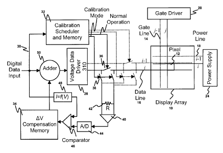
to prioritize pixels for calibration based on display and previous calibration
data, the
priority list being used to select one or more (n) pixels which are programmed
with
currents higher than a threshold current for calibration; selecting n pixels
in a selected
to column of the display array from the linked list; implementing programming
to the
pixels in the selected column, including: monitoring a pixel current for the n
pixels and
obtaining calibration data; updating a compensation memory based on the
calibration
data for calibration; sorting the priority list for the next programming.
[0008] In accordance with a further aspect of the present invention there is
provided a
15 system for real-time calibration for a display array having a plurality of
pixel circuits
arranged in row and column, each pixel circuit having a light emitting device
and a
driving transistor, the system including: a calibration scheduler for
controlling
programming and calibration of the display array, including: a priority list
for listing
one or more pixels for calibration based on display data; module for enabling,
during a
2o programming cycle, calibration mode for one or more pixels in the selected
column,
which are selected from the priority list, and during a programming cycle,
enabling
normal operation mode for the rest of the pixels in the selected column; a
monitor for
monitoring a pixel current for the pixels in the calibration mode through the
selected
column; a generator for generating a calibration data based on the monitoring
result; a
25 memory for storing calibration data; and an adjuster for adjusting a
programming data
applied to the display array based on the calibration data when the pixel on
the normal
operation mode is programmed.
[0009] In accordance with a further aspect of the present invention there is
provided a
system for a display array having a pixel circuit, the pixel circuit being
programmed
3o through a data line, the system including: a data source for providing a
programming
-2-
CA 02526782 2005-12-15
data into the pixel circuit; a current-controlled voltage source associated
with the
voltage source for converting a current on the data line to a voltage
associated with the
current to extract a time dependent parameter of the pixel circuit.
[0010] In accordance with a further aspect of the present invention there is
provided a
system for a display array including a plurality of pixel circuits, each pixel
circuit
including a driving transistor, at least one switch transistor, a storage
capacitor and a
light emitting device, the system including: a monitor for monitoring a
current or
voltage on the pixel circuit; a data process unit for controlling the
operation of the
display array, the data process unit extracting information on an aging of the
pixel
to circuit, based on the monitored current or voltage and determining a state
of the pixel
circuit; a driver controlled by the data process unit and for providing
programming and
calibration data to the pixel circuit, based on the state of the pixel
circuit.
[0011] In accordance with a further aspect of the present invention there is
provided a
method of driving a display array, the display array including a plurality of
pixel circuits,
15 each pixel circuit including a driving transistor, at least one switch
transistor, a storage
capacitor and a light emitting device, the method including the steps of-.
applying a
current or voltage to the pixel circuit; monitoring a current or voltage
flowing through
the pixel circuit; extracting information on an aging of the pixel circuit,
based on the
monitored current or voltage and determining the state of the pixel circuit;
providing
20 operation voltage to the pixel circuit, including determining programming
and
calibration data for the pixel circuit based on the state of the pixel
circuit.
[0012] In accordance with a further aspect of the present invention there is
provided a
method of driving a display array, the display array including a plurality of
pixel circuits,
each pixel circuit including a driving transistor, at least one switch
transistor, a storage
25 capacitor and a light emitting device, the method including the steps of-.
applying a
current or voltage to the light emitting device; monitoring a current or
voltage flowing
through the light emitting device; predicting a shift in the voltage of the
light emitting
device, based on the monitored current or voltage and determining the state of
the pixel
circuit; and providing, to the light emitting device, a bias associated with
the shift in the
3o voltage of the light emitting device.
-3-
CA 02526782 2005-12-15
[0013] In accordance with a further aspect of the present invention there is
provided a
system for driving a display array, the display array including a plurality of
pixel circuits,
each pixel circuit including a driving transistor, at least one switch
transistor, a storage
capacitor and a light emitting device, the system including: a monitor for
monitoring a
current or voltage on the pixel circuit; a data process unit for predicting a
shift in the
voltage of the light emitting device, based on the monitored current or
voltage and
determining the state of the pixel circuit; and a circuit for providing, to
the light
emitting device, a bias associated with the shift in the voltage of the light
emitting
device.
[0014) In accordance with an aspect of the present invention there is provided
a system
for a display array including a plurality of pixel circuits, each pixel
circuit having a
driving transistor, at least one switch transistor, a storage capacitor and a
light emitting
device, the light emitting device being located at a programming path for
programming
the pixel circuit, the system including: a controller for controlling the
operation of the
display array; a driver for providing operation voltage to the pixel circuit
based on the
control of the controller; and the driver providing the operation voltage to
the pixel
circuit during a programming cycle such that the light emitting device being
removed
from the programming path.
[0015] This summary of the invention does not necessarily describe all
features of the
invention.
[0016] Other aspects and features of the present invention will be readily
apparent to
those skilled in the art from a review of the following detailed description
of preferred
embodiments in conjunction with the accompanying drawings.
BRIEF DESCRIPTION OF THE DRAWINGS
[0017] These and other features of the invention will become more apparent
from the
following description in which reference is made to the appended drawings
wherein:
[0018] Figure 1 is a flow chart showing a process for calibration-scheduling
in
accordance with an embodiment of the present invention;
-4-
CA 02526782 2005-12-15
[0019] Figure 2 is a diagram showing an example of a system structure for
implementing the calibration-scheduling of Figure 1;
[0020] Figure 3 is a diagram showing a system architecture for a voltage-
extracting,
programming and driving in accordance with an embodiment of the present
invention;
[0021 ] Figure 4 is a diagram showing an example of the extracting,
programming and
driving system of Figure 3 and a pixel circuit;
[0022] Figure 5 is a diagram showing a further example of the extracting,
programming
and driving system of Figure 3 and a pixel circuit;
[0023] Figure 6 is a diagram showing a further example of the extracting,
programming
and driving system of Figure 3 and a pixel circuit;
[0024] Figure 7 is a diagram showing a further example of the extracting,
programming
and driving system of Figure 3 and a pixel circuit;
[0025] Figure 8 is a diagram showing a pixel circuit to which a step-
calibration driving
in accordance with an embodiment of the present invention is applied;
[0026] Figure 9 is a diagram showing an example of a driver and extraction
block and
the driving transistor of Figure 8;
[0027] Figure 10 is a diagram showing an example of an extraction algorithm
implemented by a DPU block of Figure 9;
[0028] Figure 11 is a diagram showing a further example of the extraction
algorithm
2o implemented by the DPU block of Figure 9;
[0029] Figure 12 is a timing diagram showing an example of waveforms for the
step-calibration driving;
[0030] Figure 13 is a timing diagram showing a further example of waveforms
for the
step-calibration driving;
[0031 ] Figure 14 is a diagram showing a pixel circuit to which the step-
calibration
driving is applicable;
-5-
CA 02526782 2005-12-15
[0032] Figure 15 is a graph showing the results of simulation for the step-
calibration
driving;
[0033] Figure 16 is a diagram showing an example of a system architecture for
the
step-calibration driving with a display array;
[0034] Figure 17 is a timing diagram showing an example of waveforms applied
to the
system architecture of Figure 16;
[0035] Figure 18 is a timing diagram showing an example of waveforms for a
voltage/current extraction;
[0036] Figure 19 is a timing diagram showing a further example of waveforms
for the
voltage/current extraction;
[0037] Figure 20 is a diagram showing a pixel circuit to which the
voltage/current
extraction of Figure 19 is applicable;
[0038] Figure 21 is a timing diagram showing a further example of waveforms
for the
voltage/current extraction;
[0039] Figure 22 is a diagram showing a pixel circuit to which the
voltage/current
extraction of Figure 21 is applicable;
[0040] Figure 23 is a diagram showing a mirror based pixel circuit to which
OLED
removing in accordance with an embodiment of the present invention is applied;
[0041 ] Figure 24 is a diagram showing a programming path of Figure 23 when
applying
the OLED removing;
[0042] Figure 25 is a diagram showing an example of a system architecture for
the
OLED removing; and
[0043] Figure 26 is a graph showing the simulation result for the voltage on
IDATA
line for different threshold voltage.
DETAILED DESCRIPTION OF THE PREFERRED EMBODIMENTS OF THE
INVENTION
-6-
CA 02526782 2005-12-15
[0044] Embodiments of the present invention are described using a pixel
including a
light emitting device and a plurality of transistors. The light emitting
device may be an
organic light emitting diode (OLED). It is noted that "pixel" and "pixel
circuit" may be
used interchangeably.
[0045] Real-time calibration-scheduling for a display array having a plurality
of pixels
is described in detail. Figure 1 illustrates a process for a calibration-
scheduling in
accordance with an embodiment of the present invention. According to this
technique,
the pixels are calibrated based on their aging and/or usage during the normal
operation
of the display array.
[0046] A linked list of pixels is generated in step S2. The linked list
contains an
identification of a pixel with high brightness for calibration. The linked
list is used to
schedule the priority in calibration.
[0047] In step S4, "n" is chosen based on the display size and expected
instability with
time (e.g. shift in characteristics of transistors and light emitting device).
"n" represents
the number of pixels that are calibrated in each programming cycle. "n" may be
one or
more than one.
[0048] Then programming cycle starts at step S6. The step S6 includes steps S8-
516.
The steps S8-S 16 are implemented on a selected column of the display array.
[0049] In step S8, "n" pixels in the selected column are selected from the
beginning of
2o the linked list, hereinafter referred to as "Selected Pixels".
[0050] In step S 10, "Calibration Mode" is enabled for the Selected Pixels,
and "Normal
Operation Mode" is enabled for the rest of the pixels in the selected column
of the
display array.
[0051] In step 512, all pixels in the selected column are programmed by a
voltage
source driver (e.g. 28 of Figure 2) which is connected to a data line of the
pixel.
[0052] For the Selected Pixels, current flowing through the data line is
monitored
during the programming cycle. For the pixels other than the Selected Pixels in
the
selected column, the corresponding programming voltage is boosted using data
stored
CA 02526782 2005-12-15
in a memory (e.g. 34 of Figure 2), hereinafter referred to as "0V compensation
memory".
[0053] In step S14, the monitored current is compared with the expected
current that
must flow through the data line. Then, a calibration data curve for the
Selected Pixels
is generated. The OV compensation memory is updated based on the calibration
data
curve.
[0054] The calibration data curve stored in the OV compensation memory for a
pixel
will be used to boost programming voltage for that pixel in the next
programming
cycles when that pixel is in the Normal Operation Mode.
[0055] In step 516, the identifications of the Selected Pixels are sent to the
end of the
linked list. The Selected Pixels have the lowest priority in the linked list
for calibration.
[0056] During display operation (S6-S16), the linked list will provide a
sorted priority
list of pixels that must be calibrated. It is noted that in the description,
the term "linked
list" and the term "priority list" may be used interchangeably.
[0057] The operation goes back (S18) to the step S8. The next programming
cycle
starts. A new column in the display array is activated (selected), and, new
"n" pixels in
the new activated column are selected from the top of the linked list. The 0V
compensation memory is updated using the calibration data obtained for the new
Selected Pixels.
[0058] The number of the Selected Pixels, "n", is now described in detail. As
described
above, the number "n" is determined based on the display size and expected
instability
in device characteristics with time. It is assumed that the total number of
pixels N is N
= 3xm1xm2, where ml and m2 are the number of rows and columns in the display,
respectively.
[0059] The highest rate in characteristics shift is K (=~I/Ot.I). Each
programming cycle
takes t=1/f.mz. The maximum expected shift in characteristics after the entire
display is
calibrated is DI/I = K.t.N/n < e, where a is the allowed error. After this the
calibration
can be redone from the beginning, and the error is eliminated. This shows that
n >
K.t.N/e or n > 3.K.m1/f.e. For instance, if K =1 %/hr, ml = 1024, f = 60 Hz,
and a
_g_
CA 02526782 2005-12-15
=0.1 %, then n > 0.14, which implies that it is needed to calibrate once in 5
programming
cycles. This is achievable with one calibration unit, which operates only one
time in 5
programming cycles. Each calibration unit enables calibration of one pixel at
a
programming cycle. If a = 0.01%, n > 1.4. This means that two calibration
units
calibrating two pixels in each programming cycle are required. This shows that
it is
feasible to implement this calibration system with very low cost.
[0060] The frequency of calibration can be reduced automatically as the
display ages,
since shifts in characteristics will become slower as the time progresses. In
addition,
the pixels that are selected for calibration can be programmed with different
currents
to depending on display data. The only condition is that their programming
current is
larger than a reference current. Therefore, the calibration can be performed
at multiple
brightness levels for one pixel to achieve higher accuracy.
[0061] The linked list is described in detail. In the linked list, the pixels
with high
brightness for calibration are listed. The display data is used to determine
the pixels
with high brightness for calibration. Calibration at low currents is slow and
often not
accurate. In addition, maximum shift in characteristics occurs for pixels with
high
current. Thus, in order to improve the accuracy and speed of calibration, the
pixels,
which must be programmed with currents higher than a threshold current ITH,
are
selected and stored in the linked list.
[0062] ITH is a variable and may be "0". For ITH = 0, all pixels are listed in
the linked
list, and the calibration is performed for all pixels irrespective of their
programming
current.
[0063] The calibration-scheduling technique described above is applicable to
any
current programmed pixels, for example, but not limited to, a current mirror
based
pixel.
[0064] Figure 2 illustrates an example of a system structure for implementing
the
calibration-scheduling of Figure 1. A system 30 of Figure 2 for implementing
calibration-scheduling algorithm is provided to a display array 10 having a
plurality of
pixel circuits 12. The pixel circuit 12 is a current programmed pixel circuit,
such as, but
-9-
CA 02526782 2005-12-15
not limited to a current mirror based pixel. The pixel circuits 12 are
arranged in row and
column.
[0065] The pixel circuit 12 may include an OLED and a plurality of transistors
(e.g.
TFTs). The transistor may be fabricated using amorphous silicon, nano/micro
crystalline silicon, poly silicon, organic semiconductors technologies (e.g.
organic
TFT), NMOS/PMOS technology or CMOS technology (e.g. MOSFET). The display
array 10 may be an AMOLED display array.
[0066] The pixel circuit 12 is operated by a gate line 14 connected to a gate
driver 20,
a data line 16 connected to a voltage data driver 28, and a power line
connected to a
power supply 24. In Figure 2, two data lines, two gate lines and two power
lines are
shown as an example. It is apparent that more than two data lines, two gate
lines and
two power lines may be provided to the display array 10.
[0067] The system 30 includes a calibration scheduler and memory block 32 for
controlling programming and calibration of the display array 10, and a 0V
compensation memory 34 for storing 4V compensation voltage (value). In each
programming cycle, a column of the display array 10 is selected. The
calibration
scheduler and memory block 32 enables Normal Operation Mode or Calibration
Mode
for the selected column (i.e., data line) during that programming cycle.
[0068] The system 30 further includes a monitoring system for monitoring and
measuring a pixel current. The monitoring system includes switches 36 and 38
and a
voltage sensor 40 with an accurate resistor 42. In Figure 2, the switches 36
and 38 are
provided for each data line as an example.
[0069] The system 30 further includes a generator for generating OV
compensation
voltage based on the monitoring result. The generator includes an
analog/digital
converter (A/D) 44, a comparator 46, and a translator 48. The A/D 44 converts
the
analog output of the voltage sensor 40 into a digital output. The comparator
46
compares the digital output to an output from the translator 48. The
translator 48
implements function f(V) on a digital data input 52. The translator 48
converts the
current data input 52 to the voltage data input through f(v). The result of
the
3o comparison by the comparator 46 is stored in the OV compensation memory 34.
-t 4
CA 02526782 2005-12-15
[0070] The system 30 further includes an adder 50 for adding the digital data
input 52
and the 0V compensation voltage stored in the OV compensation memory 34. The
voltage data driver 28 drives a data line based on the output of the adder 50.
The
programming data for the data line is adjusted by adding the 0V compensation
voltage.
[0071 ] When the calibration scheduler and memory block 32 enables the Normal
Operation Mode for a selected data line, the switch 36 is activated. The
voltage output
from the voltage data driver 28 is directly applied to the pixel on that data
line.
[0072] When the calibration scheduler and memory block 32 enables the
Calibration
Mode for that data line, the switch 38 is activated. The voltage is applied to
the pixel
on that data line through the accurate resistor 42. The voltage drop across
the resistor
42 at the final stages of the programming time (i.e. when initial transients
are finished)
is measured by the voltage sensor 40. The voltage drop monitored by the
voltage sensor
40 is converted to digital data by the A/D 44. The resulting value of the
voltage drop is
proportional to the current flowing through the pixel if the pixel is a
current
programmed pixel circuit. This value is compared by the comparator 46 to the
expected
value obtained by the translator 48.
[0073] The difference between the expected value and the measured value is
stored in
the 0V compensation memory 34, and will be used for a subsequent programming
cycle. The difference will be used to adjust the data voltage for programming
of that
2o pixel in future.
[0074] The calibration scheduler and memory block 32 may include the linked
list
described above. In the beginning, the linked list is generated automatically.
It may be
just a list of pixels. However, during the operation it is modified.
[0075] The calibration of the pixel circuits with high brightness guarantees
the high
speed and accurate calibration that is needed in large or small area displays.
[0076] Since the display array 10 is driven using a voltage programming
technique, it is
fast and can be used for high-resolution and large area displays.
CA 02526782 2005-12-15
[0077] Due to speed, accuracy, and ease of implementation, the applications of
the
calibration-scheduling technique ranges from electroluminescent devices used
for
cellphones, personal organizers, monitors, TVs, to large area display boards.
[0078] The system 30 monitors and measures voltage drop which depends on time
dependent parameters of the pixel, and generates a desirable programming data.
However, the time dependent parameters of the pixel may be extracted by any
mechanisms other than that of Figure 2.
[0079] A further technique for programming, extracting time dependent
parameters of
a pixel and driving the pixel is described in detail with reference to Figures
3-7. This
technique includes voltage-extracting for calibration. Programming data is
calibrated
with the extracted information, resulting in a stable pixel current over time.
Using this
technique, the aging of the pixel is extracted.
[0080] Figure 3 illustrates a system architecture for implementing a voltage-
extracting,
programming and driving in accordance with an embodiment of the present
invention.
The system of Figure 3 implements the voltage-extracting and programming to a
current mode pixel circuit 60. The pixel circuit 60 includes a light emitting
device and
a plurality of transistors having a driving transistor (not shown). The
transistors may be
TFTs.
[0081] The pixel circuit 60 is selected by a select line SEL and is driven by
DATA on
2o a data line 61. A voltage source 62 is provided to write a programming
voltage VP into
the pixel circuit 60. A current-controlled voltage source (CCVS) 63 having a
positive
node and a negative node is provided to convert the current on the data line
61 to a
voltage Vext. A display controller and scheduler 64 operates the pixel circuit
60. The
display controller and scheduler 64 monitors an extracted voltage Vext output
from the
CCVS 63 and then controls the voltage source 62.
[0082] The resistance of CCVS 63 is negligible. Thus the current on the data
line 61 is
written as:
_ 2
lLine lpiexl -~ (VP-VT) ...(1)
CA 02526782 2005-12-15
where ILi"e represents the current on the data line 61, Ip;eX; represents a
pixel current, VT
represents the threshold voltage of the driving transistor included in the
pixel circuit 60,
and (3 represents the gain parameter in the TFT characteristics.
[0083] As the threshold voltage of the driving TFT increases during the time,
the
current on the data line 61 decreases. By monitoring the extracted voltage
Vext, the
display controller and scheduler 64 determines the amount of shift in the
threshold
voltage.
[0084] The threshold voltage VT of the driving transistor can be calculate as:
VT - VP-~ILine~y0.5 ...~2~
[0085] The programming voltage VP is modified with the extracted information.
The
extraction procedure can be implemented for one or several pixels during each
frame
time.
[0086] Figure 4 illustrates an example of a system for the voltage-extracting,
programming and driving of Figure 3, which is employed with a top-emission
current-cell pixel circuit 70. The pixel circuit 70 includes an OLED 71, a
storage
capacitor 72, a driving transistor 73 and switch transistors 74 and 75.
[0087] The transistors 73, 74 and 75 may be n-type TFTs. However, these
transistors
73, 74 and 75 may be p-type transistors. The voltage-extracting and
programming
technique applied to the pixel circuit 70 is also applicable to a pixel
circuit having
2o p-type transistors.
[0088] The driving transistor 73 is connected to a data line 76 through the
switch
transistor 75, and is connected to the OLED 71, and also is connected to the
storage
capacitor 72 through the switch transistor 74. The gate terminal of the
driving transistor
73 is connected to the storage capacitor 72. The gate terminals of the switch
transistors
74 and 75 are connected to a select line SEL. The OLED 71 is connected to a
voltage
supply electrode or line VDD. The pixel circuit 70 is selected by the select
line SEL and
is driven by DATA on the data line 76.
~3
CA 02526782 2005-12-15
[0089] A current conveyor (CC) 77 has X, Y and Z terminals, and is used to
extract a
current on the data line 76 without loading it. A voltage source 78 applies
programming
voltage to the Y terminal of the CC 77. In the CC 77, the X terminal is forced
by
feedback to have the same voltage as that of the Y terminal. Also, the current
on the
X terminal is duplicated into the Z terminal of the CC 77. A current-
controlled voltage
source (CCVS) 79 has a positive node and a negative node. The CCVS 79 converts
the
current on the Z terminal of the CC 77 into a voltage Vext.
[0090] Vext is provided to the display controller and scheduler 64 of Figure
3, where
the threshold voltage of the driving transistor 73 is extracted. The display
controller
to and scheduler 64 controls the voltage source 78 based on the extracted
threshold
voltage.
[0091] Figure 5 illustrates a further example of a system for the voltage-
extracting,
programming, and driving of Figure 3, which is employed with a bottom-emission
current-cell pixel circuit 80. The pixel circuit 80 includes an OLED 81, a
storage
capacitor 82, a driving transistor 83, and switch transistors 84 and 85. The
transistors
83, 84 and 85 may be n-type TFTs. However, these transistors 83, 84 and 85 may
be
p-type transistors.
[0092] The driving transistor 83 is connected to a data line 86 through the
switch
transistor 85, and is connected to the OLED 81, and also is connected to the
storage
2o capacitor 82. The gate terminal of the driving transistor 83 is connected
to a voltage
supply line VDD through the switch transistor 84. The gate terminals of the
switch
transistors 84 and 85 are connected to a select line SEL. The pixel circuit 80
is selected
by the select line SEL and is driven by DATA on the data line 86.
[0093] A current conveyor (CC) 87 has X, Y and Z terminals, and is used to
extract a
current on the data line 86 without loading it. A voltage source 88 applies a
negative
programming voltage at the Y terminal of the CC 87. In the CC 87, the X
terminal is
forced by feedback to have the same voltage as that of the Y terminal. Also,
the current
on the X terminal is duplicated into the Z terminal of the CC 87. A current-
controlled
voltage source (CCVS) 89 has a positive node and a negative node. The CCVS 89
converts the current of the Z terminal of the CC 87 into a voltage Vext.
CA 02526782 2005-12-15
[0094] Vext is provided to the display controller and scheduler 64 of Figure
3, where
the threshold voltage of the driving transistor 83 is extracted. The display
controller
and scheduler 64 controls the voltage source 88 based on the extracted
threshold
voltage.
[0095] Figure 6 illustrates a further example of a system for the voltage-
extracting,
programming and driving of Figure 3, which is employed with a top-emission
current-mirror pixel circuit 90. The pixel circuit 90 includes an OLED 91, a
storage
capacitor 92, mirror transistors 93 and 94, and switch transistors 95 and 96.
The
transistors 93, 94, 95 and 96 may be n-type TFTs. However, these transistors
93, 94, 95
to and 96 may be p-type transistors.
[0096] The mirror transistor 93 is connected to a data line 97 through the
switch
transistor 95, and is connected to the storage capacitor 92 through the switch
transistor
96. The gate terminals of the mirror transistors 93 and 94 are connected to
the storage
capacitor 92 and the switch transistor 96. The mirror transistor 94 is
connected to a
voltage supply electrode or line VDD through the OLED 91. The gate terminals
of the
switch transistors 85 and 86 are connected to a select line SEL. The pixel
circuit 90 is
selected by the select line SEL and is driven by DATA on the data line 97.
[0097] A current conveyor (CC) 98 has X, Y and Z terminals, and is used to
extract the
current of the data line 97 without loading it. A voltage source 99 applies a
positive
2o programming voltage at the Y terminal of the CC 98. In the CC 98, the X
terminal is
forced by feedback to have the same voltage as the voltage of the Y terminal.
Also, the
current on the X terminal is duplicated into the Z terminal of the CC 98. A
current-controlled voltage source (CCVS) 100 has a positive node and a
negative node.
The CCVS 100 converts a current on the Z terminal of the CC 98 into a voltage
Vext.
[0098] Vext is provided to the display controller and scheduler 64 of Figure
3, where
the threshold voltage of the driving transistor 93 is extracted. The display
controller
and scheduler 64 controls the voltage source 99 based on the extracted
threshold
voltage.
[0099] Figure 7 illustrates a further example of a system for the voltage-
extracting,
3o programming and driving of Figure 3, which is employed with a bottom-
emission
CA 02526782 2005-12-15
current-mirror pixel circuit 110. The pixel circuit 110 includes an OLED 111,
a storage
capacitor 112, mirror transistors 113 and 116, and switch transistors 114 and
115. The
transistors 113, 114, 115 and 116 may be n-type TFTs. However, these
transistors 113,
114, 115 and 116 may be p-type transistors.
[00100] The mirror transistor 113 is connected to a data line 117 through the
switch transistor 114, and is connected to the storage capacitor 112 through
the switch
transistor 115. The gate terminals of the mirror transistors 113 and 116 are
connected
to the storage capacitor 112 and the switch transistor 115. The mirror
transistor 116 is
connected to a voltage supply line VDD. The mirror transistors 113, 116 and
the
1o storage capacitor 112 are connected to the OLED 111. The gate terminals of
the switch
transistors 114 and 115 are connected to a select line SEL. The pixel circuit
110 is
selected by the select line SEL and is driven by DATA on the data line 117.
[00101] A current conveyor (CC) 118 has X, Y and Z terminals, and is used to
extract the current of the data line 117 without loading it. A voltage source
119 applies
a positive programming voltage at the Y terminal of the CC 118. In the CC 118,
the X
terminal is forced by feedback to have the same voltage as the voltage of the
Y terminal
of the CC 118. Also, the current on the X terminal is duplicated into the Z
terminal of
the CC 118. A current-controlled voltage source (CCVS) 120 has a positive node
and
a negative node. The 120 converts the current on the Z terminal of the CC 118
into a
voltage Vext.
[00102] Vext is provided to the display controller and scheduler 64 of Figure
3,
where the threshold voltage of the driving transistor 113 is extracted. The
display
controller and scheduler 64 controls the voltage source 119 based on the
extracted
threshold voltage.
[00103] Refernng to Figures 3-7, using the voltage-extracting technique, time
dependent parameters of a pixel (e.g. threshold shift) can be extracted. Thus,
the
programming voltage can be calibrated with the extracted information,
resulting in a
stable pixel current over time. Since the voltage of the OLED (i.e. 71 of
Figure 4, 81 of
Figure 5, 91 of Figure 6, 111 of Figure 7) affects the current directly, the
~6
CA 02526782 2005-12-15
voltage-extracting driving technique described above can also be used to
extract OLED
degradation as well as the threshold shift.
[00104] The voltage-extracting technique described above can be used with any
current-mode pixel circuit, including current-mirror and current-cell pixel
circuit
architectures, and are applicable to the display array 10 of Figure 2. A
stable current
independent of pixel aging under prolonged display operation can be provided
using the
extracted information. Thus, the display operating lifetime is efficiently
improved.
[00105] It is noted that the transistors in the pixel circuits of Figures 3-7
may be
fabricated using amorphous silicon, nano/micro crystalline silicon, poly
silicon, organic
to semiconductors technologies (e.g. organic TFT), NMOS/PMOS technology or
CMOS
technology (e.g. MOSFET). The pixel circuits of Figures 3-7 may form AMOLED
display arrays.
[00106] A further technique for programming, extracting time dependent
parameters of a pixel and driving the pixel is described in detail with
reference to
15 Figures 8-17. The technique includes a step-calibration driving technique.
In the
step-calibration driving technique, information on the aging of a pixel (e.g.
threshold
shift) is extracted. The extracted information will be used to generate a
stable pixel
current/luminance. Despite using the one-bit extraction technique, the
resolution of the
extracted aging is defined by display drivers. Also, the dynamic effects are
2o compensated since the pixel aging is extracted under operating condition,
which is
similar to the driving cycle.
[00107] Figure 8 illustrates a pixel circuit 160 to which a step-calibration
driving
in accordance with an embodiment of the present invention is applied. The
pixel circuit
160 includes an OLED 161, a storage capacitor 162, and a driving transistor
163 and
25 switch transistors 164 and 165. The pixel circuit 160 is a current-
programmed, 3-TFT
pixel circuit. A plurality of the pixel circuits 160 may form an AMOLED
display.
[00108] The transistors 163, 164 and 165 are n-type TFTs. However, the
transistors 163, 164 and 165 may be p-type TFTs. The step-calibration driving
technique applied to the pixel circuit 160 is also applicable to a pixel
circuit having
3o p-type transistors. The transistors 163, 164 and 165 may be fabricated
using amorphous
CA 02526782 2005-12-15
silicon, nano/micro crystalline silicon, poly silicon, organic semiconductors
technologies (e.g. organic TFT), NMOS/PMOS technology or CMOS technology (e.g.
MOSFET).
[00109] The gate terminal of the driving transistor 163 is connected to a
signal
line VDATA through the switch transistor 164, and also connected to the
storage
capacitor 162. The source terminal of the driving transistor 163 is connected
to a
common ground. The drain terminal of the driving transistor 163 is connected
to a
monitor line MONITOR through the switch transistor 165, and also is connected
to the
cathode electrode of the OLED 161.
[00110] The gate terminal of the switch transistor 164 is connected to a
select
line SEL1. The source terminal of the switch transistor 164 is connected to
the gate
terminal of the driving transistor 163, and is connected to the storage
capacitor 162.
The drain terminal of the switch transistor 164 is connected to VDATA.
[00111 ] The gate terminal of the switch transistor 165 is connected to a
select
line SEL2. The source terminal of the switch transistor 165 is connected to
MONITOR.
The drain terminal of the switch transistor 165 is connected to the drain
terminal of the
driving transistor 163 and the cathode electrode of the OLED 161. The anode
electrode
of the OLED 161 is connected to a voltage supply electrode or line VDD.
[00112] The transistors 163 and 164 and the storage capacitor 162 are
connected
at node A3. The transistors 163 and 165 and the OLED 161 are connected at node
B3.
[00113] Figure 9 illustrates an example of a driver and extraction block 170
along with the driving transistor 163 of Figure 8. In Figure 9, each of Rs 171
a and Rs
171b represents the ON resistance of the switch transistors (e.g. 164, 165 of
Figure 8).
Cs represents the storage capacitor of the pixel, CoLED represents the OLED
capacitance, and CP represents the line parasitic capacitance. In Figure 9,
the OLED is
presented as a capacitance.
[00114] A block 173 is used to extract the threshold voltage of the driving
transistor, during the extraction cycle. The block 173 may be a current sense
amplifier
CA 02526782 2005-12-15
(SA) or a current comparator. In the description, the block 173 is referred to
as "SA
block 173".
[00115] If the current of the MONITOR line is higher than a reference current
(IREF), the output of the SA block 173 (i.e. Triggers of Figure 10, 11)
becomes one. If
the current of the MONITOR line is less than the reference current (IREF), the
output
of the SA block 173 becomes zero.
[00116] It is noted that the SA block 173 can be shared between few columns
result in less overhead. Also, the calibration of the pixel circuit can be
done one at a
time, so the extraction circuits can be shared between the all columns.
to [00117] A data process unit (DPU) block 172 is provided to control the
programming cycle, contrast, and brightness, to perform the calibration
procedure and
to control the driving cycle. The DPU block 172 implements extraction
algorithm to
extract (estimate) the threshold voltage of the driving transistor based on
the output
from the SA block 173, and controls a driver 174 which is connected to the
driving
transistor 163.
[00118] Figure 10 illustrates an example of the extraction algorithm
implemented by the DPU block 172 of Figure 9. The algorithm of Figure 10 is in
a part
of the DPU block 172. In Figure 10, VT(i, j) represents the extracted
threshold voltage
for the pixel (i, j) at the previous extraction cycle, Vs represents the
resolution of the
2o driver 174, "i" represents a row of a pixel array and "j" represents a
column of a pixel
array. Trigger conveys the comparison results of the SA block 173 of Figure 9.
Less state 180 determines the situation in which the actual VT of the pixel is
less than
the predicted VT (VTM), Equal state 181 determines the situation in which the
predicted
VT (VTM) and the actual VT of the pixel are equal, and Great state 182
determines the
situation in which the actual VT of the pixel is greater than the predicted VT
(VTM).
[00119] The DPU block 172 of Figure 9 determines an intermediate threshold
voltage VTM as follows:
(Al) When s(i, j)=Less state (180), the actual threshold voltage is less than
VT(i, j),
VTM is set to (VT (i, j)-Vs).
.t 9
CA 02526782 2005-12-15
(A2) When s(i, j)=Equal state (181), the actual threshold voltage is equal to
VT(i, j),
VTM is set to VT (i, j).
(A3) When s(i, j)=Greater state (182), the actual threshold voltage is greater
than
VT(i, j), VTM is set to (VT(i, j)+ Vs).
where s(i, j) represents the previous state of the pixel (i, j) stored in a
calibration
memory (e.g. 208 of Figure 16).
[00120] Figure 11 illustrates a further example of the extraction algorithm
implemented by the DPU block 172 of Figure 9. The algorithm of Figure 11 is in
a part
of the DPU block 172 of Figure 9. In Figure 11, VT(i, j) represents the
extracted
to threshold voltage for the pixel (i, j) at the previous extraction cycle, Vs
represents the
resolution of the driver 174, "i" represents a row of a pixel array and "j"
represents a
column of a pixel array. Trigger conveys the comparison results of the SA
block 173.
[00121] Further, in Figure 11, Vres represents the step that will be
added/subtracted to the predicted VT (VTM) in order achieve the actual VT of
the pixel,
A represents the reduction gain of a prediction step, and K represents the
increase gain
of the prediction step.
[00122] The operation of Figure 11 is the same as that of Figure 10, except
that
it has gain extra states L2 and G2 for rapid extraction of abrupt changes. In
the gain
states, the step size is increased to follow the changes more rapidly. L1 and
G1 are the
2o transition states which define the VT change is abrupt or normal.
[00123] Figure 12 illustrates an example of waveforms applied to the pixel
circuit 160 of Figure 8. In Figure 12, V~all=Va+VTM , and VDR =VP+ VT(i, j)
+V~F,
where VB represents the bias voltage during the extraction cycle, VTM is
defined based
on the algorithm shown in Figure 10 or 1 l, VP represents a programming
voltage, VT(i,
j) represents the extracted threshold voltage at the previous extraction
cycle, VHF
represents the source voltage of the driving transistor during the programming
cycle.
[00124] Referring to Figures 8-12, the operation of the pixel circuit 160
includes
operating cycles X51, X52, X53, and X54 . In Figurel2, an extraction cycle is
separated from a programming cycle. The extraction cycle includes X51 and X52,
and
~4
CA 02526782 2005-12-15
the programming cycle includes X53. X54 is a driving cycle. At the end of the
programming cycle, node A3 is charged to (VP+ VT) where VP is a programming
voltage and VT is the threshold voltage of the driving transistor 163.
[00125] In the first operating cycle X51: SEL1 and SEL 2 are high. Node A3 is
charged to V~a~, and node B3 is charged to VHF. V~a~ is VB+VTM in which VB is
a bias
voltage, and VTM the predicted VT, and VHF should be larger than VDD-VoLEDO
where
VOLEDO 1S the ON voltage of the OLED 161.
[00126] In the second operating cycle X52: SEL1 goes to zero. The gate-source
voltage of the driving transistor 163 is given by:
1 o VGS=Vg+VTM+OVB+OVTM-OVT2-OVH
where VGS represents the gate-source voltage of the driving transistor 163,
~VB,
OVTM, OVT2 and 4VH are the dynamic effects depending on VB, VTM, VTa and VH,
respectively. VTZ represents the threshold voltage of the switch transistor
164, and VH
represents the change in the voltage of SEL1 at the beginning of second
operating cycle
X52 when it goes to zero.
[00127] The SA block 173 is tuned to sense the current larger than (3(VB)2, so
that
the gate-source voltage of the driving transistor 163 is larger than (Vg +VT),
where (3 is
the gain parameter in the I-V characteristic of the driving transistor 163.
[00128] As a result, after few iterations, VTM and the extracted threshold
voltage
2o VT(i, j) for the pixel (i, j) converge to:
VTM=VT- Y ~(VB+VT+VTa-VH)
_ Cgz l(2 ' Cs )
1 + Cg2 /(2 ~CS)
where Cg2 represents the gate capacitance of the switch transistor 164.
[00129] In the third operating cycle X53: SEL1 is high. VDATA goes to VDR.
Node A3 is charged to [VP+VT(i, j)-y(VP-VB)].
CA 02526782 2005-12-15
[00130] In the fourth operating cycle X54: SEL1 and SEL2 go to zero.
Considering the dynamic effects, the gate-source voltage of the driving
transistor 163
can be written as:
VGS=Vp+VT
[00131 ] Therefore, the pixel current becomes independent of the static and
dynamic effects of the threshold voltage shift.
[00132] In Figure 12, the extraction cycle and the programming cycle are shown
as separated cycles. However, the extraction cycle and the programming cycle
may be
merged as shown in Figure 13. Figure 13 illustrates a further example of
waveforms
applied to the pixel circuit 160 of Figure 8.
[00133] Referring to Figures 8-11 and 13, the operation of the pixel circuit
160
includes operating cycles X61, X62 and X63. Programming and extraction cycles
are
merged into the operating cycles X61 and X62. The operating cycle X63 is a
driving
cycle.
[00134] During the programming cycle, the pixel current is compared with the
desired current, and the threshold voltage of the driving transistor is
extracted with the
algorithm of Figure 10 or 11. The pixel circuit 160 is programmed with VDR=Vp+
VT
(i, j)+VREF during the operating cycle X61. Then the pixel current is
monitored through
the MONITOR line, and is compared with the desired current. Based on the
2o comparison result and using the extraction algorithm of Figures 10 or 11,
the threshold
voltage VT (i, j) is updated.
[00135] In Figure 8, two select lines SEL1 and SEL2 are shown. However, a
signal select line (e.g. SELI) can be used as a common select line to operate
the switch
transistors 164 and 165. When using the common select line, SEL1 of Figure 12
stays
at high in the second operating cycle X52, and the VGS remains at (VB+V~).
Therefore, the dynamic effects are not detected.
[00136] The step-calibration driving technique described above is applicable
to
the pixel circuit 190 of Figure 14. The pixel circuit 190 includes an OLED
191, a
storage capacitor 192, and a driving transistor 193 and switch transistors 194
and 195.
22
CA 02526782 2005-12-15
The pixel circuit 190 is a current-programmed, 3-TFT pixel circuit. A
plurality of the
pixel circuits 190 may form an AMOLED display.
[00137] The transistors 193, 194 and 195 are n-type TFTs. However, the
transistors 193, 194 and 195 may be p-type TFTs. The step-calibration driving
technique applied to the pixel circuit 190 is also applicable to a pixel
circuit having
p-type transistors. The transistors 193, 194 and 195 may be fabricated using
amorphous
silicon, nano/micro crystalline silicon, poly silicon, organic semiconductors
technologies (e.g. organic TFT), NMOS/PMOS technology or CMOS technology (e.g.
MOSFET).
l0 [00138] The gate terminal of the driving transistor 193 is connected to a
signal
line VDATA through the switch transistor 194, and also connected to the
storage
capacitor 192. The source terminal of the driving transistor 193 is connected
to the
anode electrode of the OLED 191, and is connected to a monitor line MONITOR
through the switch transistor 195. The drain terminal of the driving
transistor 193 is
connected to a voltage supply line VDD. The gate terminals of the transistors
194 and
195 are connected to select lines SELL and SEL2, respectively.
[00139] The transistors 193 and 194 and the storage capacitor 192 are
connected
at node A4. The transistor 195, the OLED 191 and the storage capacitor 192 are
connected at node B4.
[00140] The structure of the pixel circuit 190 is similar to that of Figure 8,
except
that the OLED 191 is at the source terminal of the driving transistor 193. The
operation
of the pixel circuit 190 is the same as that of Figure 12 or 13.
[00141 ] Since the source terminal of the drive TFT 193 is forced to VREF
during
the extraction cycle (X51 and X52 or X62), the extracted data is independent
of the
ground bouncing. Also, during the programming cycle (X53 or X61), the source
terminal of the drive TFT is forced to VREF, the gate-source voltage of the
drive TFT
becomes independent of the ground bouncing. As a result of these conditions,
the pixel
current is independent of ground bouncing.
~3
CA 02526782 2005-12-15
[00142] Figure 1 S illustrates the results of simulation for the step-
calibration
driving technique. In Figure 15, "Case I" represents an operation of Figure 8
where
SEL1 goes to zero in the second operating cycle (X52 of Figure 12); "Case II"
represents an operation of Figure 8 where SEL1 stays at high in the second
operating
cycle.
[00143] In Figure 15, OVTR is the minimum detectable shift in the threshold
voltage of the driving transistor (e.g. 163 of Figure 8), OVTZR 1S the minimum
detectable
shift in the threshold voltage of the switch transistor (e.g. 164 of Figure
8), and IPL is the
pixel current of the pixel during the driving cycle..
to [00144] The pixel current of Case II is smaller than that of Case I for a
given
programming voltage due to the dynamic effects of the threshold voltage shift.
Also,
the pixel current of Case II increases as the threshold voltage of the driving
transistor
increases (a), and decreases as the threshold voltage of the switch transistor
decreases
(b). However, the pixel current of Case I is stable. The maximum error induced
in the
pixel current is less than %0.5 for any shift in the threshold voltage of the
driving and
switch TFTs. It is obvious that 4VTaR is larger than OVTR because the effect
of a shift
in VT on the pixel current is dominant. These two parameters are controlled by
the
resolution (Vs) of the driver (e.g. 174 of Figure 9), and the SNR of the SA
block (e.g.
193 of Figure 9). Since a shift smaller than OVTR cannot be detected, and also
the time
2o constant of threshold-shift is large, the extraction cycles (e.g. X51, X52
of Figure 12)
can be done after a long time interval consisting of several frames, leading
to lower
power consumption. Also, the major operating cycles become the other
programming
cycle (e.g. X53 of Figure 12) and the driving cycle (e.g. X54 of Figure 12).
As a result,
the programming time reduces significantly, providing for high-resolution,
large-area
AMOLED displays where a high-speed programming is prerequisite.
[00145] Figure 16 illustrates an example of a system architecture for the
step-calibration driving with a display array 200. The display array 200
includes a
plurality of the pixel circuits (e.g. 160 of Figure 8 or 190 of Figure 14).
[00146] A gate driver 202 for selecting the pixel circuits, a drivers/SAs
block
204, and a data process and calibration unit block 206 are provided to the
display array
~.4
CA 02526782 2005-12-15
200. The drivers/SAs block 204 includes the driver 174 and the SA block 173 of
Figure
9. The data process and calibration unit block 206 includes the DPU block 172
of
Figure 9. "Calibration" in Figure 16 includes the calibration data from a
calibration
memory 208, and may include some user defined constants for setting up
calibration
data processing. The contrast and the brightness inputs are used to adjust the
contrast
and the brightness of the panel by the user. Also, gamma-correction data is
defined
based on the OLED characteristic and human eye. The gamma-correction input is
used
to adjust the pixel luminance for human eyes.
[00147] The calibration memory 208 stores the extracted threshold voltage
1o VT(i, j) and the state s(i, j) of each pixel. A memory 210 stores the other
required data
for the normal operation of a display including gamma correction, resolution,
contrast,
and etc. The DPU block performs the normal tasks assigned to a controller and
scheduler in a display. Besides, the algorithm of Figure 10 or 11 is added to
it to
perform the calibration.
[00148] Figure 17 illustrates an example of waveforms applied to the system
architecture of Figure 16. In Figure 17, each of ROW[1], ROW[2], and ROW[3]
represents a row of the display array 200, "E" represents an extraction
operation, "P"
represents a programming operation and "D" represents a driving operation. It
is noted
that the extraction cycles (E) are not required to be done for all the frame
cycle.
Therefore, after a long time interval (extraction interval), the extraction is
repeated for
a pixel.
[00149] As shown in Figure 17, only one extraction procedure occurs during a
frame time. Also, the VT extraction of the pixel circuits at the same row is
preformed
at the same time.
[00150] Therefore, the maximum time required to refresh a frame is:
z~. - n . zP -t- z~
where it represents the frame time, iP represents the time required to write
the pixel
data into the storage capacitor (e.g. 162 of Figure 8), iE represents the
extraction time,
and n represents the number of row in the display array (e.g. 200 of Figure
16).
~S
CA 02526782 2005-12-15
[00151] Assuming iE =m~iP, the frame time iF can be written as:
zF = (h + m) wP
where m represents the timing required for the extraction cycles in the scale
of
programming cycle timing (iP).
[00152] For example, for a Quarter Video Graphics Array (QVGA) display
(240x320) with frame rate of 60Hz, if m=10, the programming time of each row
is
66~s, and the extraction time is 0.66ms.
[00153] It is noted that the step-calibration driving technique described
above is
applicable to any current-programmed pixel circuit other than those of Figures
8 and 14.
[00154] Using the step-calibration driving technique, the time dependent
parameters) of a pixel, such as threshold shift, is extracted. Then, the
programming-voltage is calibrated with the extracted information, resulting in
a stable
pixel current over time. Further, a stable current independent of the pixel
aging under
prolonged display operation can be is provided to the pixel circuit, which
efficiently
improves the display operating lifetime.
[00155] A technique for programming, extracting time dependent parameters of
a pixel and driving the pixel in accordance with a further embodiment of the
present
invention is described in detail. The technique includes extracting
information on the
aging of a pixel (e.g. OLED luminance) by monitoring OLED voltage or OLED
current,
2o and generating luminance. The programming voltage is calibrated with the
extracted
information, resulting in stable brightness over time.
[00156] Since the OLED voltage/current has been reported to be correlated with
the brightness degradation in the OLED (e.g. 161 of Figure 8, 191 of Figure
14), the
programming voltage can be modified by the OLED voltage/current to provide a
constant brightness.
[00157] For example, during the driving cycle, the voltage/current of the OLED
(161 of Figure 8 or 191 of Figure 14) is extracted while SEL2 is high. Since
the OLED
voltage or current has been reported to be correlated with the brightness
degradation in
~6
CA 02526782 2005-12-15
the OLED, the programming voltage can be modified by the OLED voltage to
provide
a constant brightness.
[00158] Figure 18 illustrates an example of waveforms for the voltage/current
extraction. The waveforms of Figure 18 are applicable to the pixel circuit 160
of Figure
8 and the pixel circuit 190 of Figure 14 to extract OLED voltage/current. The
operation
of Figure 18 includes operating cycles X71, X72 and X73. The operating cycles
X71
and X72 are an OLED extraction cycle. The operating cycle X73 is one of the
operating
cycles shown in Figure 12 and 13.
[00159] During the first operating cycle X71, SEL1 and SEL2 are high, and
l0 VDATA is zero. The gate-source voltage of the driving transistor (e.g. 163
of Figure
8) becomes zero. A current or voltage is applied to the OLED (161 of Figure 8)
through
the MONITOR line.
[00160] During the second operating cycle X72, SEL2 is high and SEL1 is low.
The OLED voltage or current is extracted through the MONITOR line using the
algorithm presented in Figures 10 or 11. This waveform can be combined with
any
other driving waveform.
[00161] In the above description, the algorithm of Figure 10 and 11 is used to
predict the aging data, i.e. VT shift, based on the comparison results
(current with
current or voltage with voltage). However, the algorithm of Figures 10 and 11
is
2o applicable to predict the shift in the OLED voltage VpLED by replacing VT
with the
VoLED and the comparison result of OLED current/voltage with a reference
current/voltage. In the description above, the system architecture shown in
Figure 9 is
used to compensate for the threshold shift. However, it is understood that the
OLED
data is also extracted when the architecture of Figure 9, i.e. DPU 172, block
173, driver
174, is used. This data can be used to compensate for the OLED shift.
[00162] The operating cycle X73 can be any operating cycle including the
programming cycle. This depends on the status of the panel after OLED
extraction. If
it is during the operation, then X73 is the programming cycle of the waveforms
in
Figures 12 and 13. The OLED voltage can be extracted during the driving cycle
X55/X63 of Figure 12/13. During the driving cycle X55/X63, the SEL2 of Figure
8 or
CA 02526782 2005-12-15
14 goes to a high voltage, and so the voltage of the OLED can be read back
through the
MONITOR for a specific pixel current.
[00163] Figure 19 illustrates a further example of waveforms for the
voltage/current extraction. Figure 20 illustrates a pixel circuit 220 to which
the
voltage/current extraction of Figure 19 is applied.
[00164] Referring to Figure 20, the pixel circuit 220 includes an OLED 221, a
storage capacitor 222, and a driving transistor 223 and switch transistors 224
and 225.
A plurality of the pixel circuits 220 may form an AMOLED display.
[00165] The transistors 223, 224 and 225 are n-type TFTs. However, the
to transistors 223, 224 and 225 may be p-type TFTs. The voltage/current
extraction
technique applied to the pixel circuit 220 is also applicable to a pixel
circuit having
p-type transistors. The transistors 223, 224 and 225 may be fabricated using
amorphous
silicon, nano/micro crystalline silicon, poly silicon, organic semiconductors
technologies (e.g. organic TFT), NMOS/PMOS technology or CMOS technology (e.g.
15 MOSFET).
[00166] The gate terminal of the driving transistor 223 is connected to the
source
terminal of the switch transistor 224, and also connected to the storage
capacitor 222.
The one terminal of the driving transistor 223 is connected to a common
ground. The
other terminal of the driving transistor 223 is connected to a monitor and
data line
2o MONITOR/DATA through the switch transistor 235, and is also connected to
the
cathode electrode of the OLED 221.
[00167] The gate terminal of the switch transistor 224 is connected to a
select
line SEL1. The one terminal of the switch transistor 224 is connected to the
gate
terminal of the driving transistor 223, and is connected to the storage
capacitor 222.
25 The other terminal of the switch transistor 224 is connected to the cathode
electrode of
the OLED 221 a
[00168] The gate terminal of the switch transistor 225 is connected to a
select
line SEL2. The one terminal of the switch transistor 225 is connected to
MONITOR/DATA. The other terminal of the switch transistor 225 is connected to
the
CA 02526782 2005-12-15
driving transistor 223 and the cathode electrode of the OLED 221. The anode
electrode
of the OLED 221 is connected to a voltage supply electrode or line VDD.
[00169] The transistors 223 and 224 and the storage capacitor 222 are
connected
at node A5. The transistors 223 and 225 and the OLED 221 are connected at node
B5.
[00170] The pixel circuit 220 is similar to the pixel circuit 160 of Figure 8.
However, in the pixel circuit 220, the MONITOR/DATA line is used for
monitoring
and programming purpose.
[00171] Refernng to Figures 19-20, the operation of the pixel circuit 220
includes operating cycles X81, X82 and X83.
to [00172] During the first operating cycle X81, SEL1 and SEL2 are high and
MONITOR/DATA is zero. The gate-source voltage of the driving transistor (223
of
Figure 20) becomes zero.
[00173] During the second operating cycle X82, a current or voltage is applied
to
the OLED through the MONITOR/DATA line, and its voltage or current is
extracted.
As described above, the shift in the OLED voltage is extracted using the
algorithm
presented in Figure 10 or 11 based on the monitored voltage or current. This
waveform
can be combined with any driving waveform.
[00174] The operating cycle X83 can be any operating cycle including the
programming cycle. This depends on the status of the panel after OLED
extraction. .
[00175] The OLED voltage/current can be extracted during the driving cycle of
the pixel circuit 220 of Figure 20 after it is programmed for a constant
current using any
driving technique. During the driving cycle the SEL2 goes to a high voltage,
and so the
voltage of the OLED can be read back through the MONITOR/DATA line for a
specific
pixel current.
[00176] Figure 21 illustrates a further example of waveforms for the
voltage/current extraction technique. Figure 22 illustrates a pixel circuit
230 to which
the voltage/current extraction of Figure 21 is applied. The waveforms of
Figure 21 is
also applicable to the pixel circuit 160 of Figure 8 to extract OLED
voltage/current.
2g
CA 02526782 2005-12-15
[00177] Referring to Figure 22, the pixel circuit 230 includes an OLED 231, a
storage capacitor 232, and a driving transistor 233 and switch transistors 234
and 235.
A plurality of the pixel circuits 230 may form an AMOLED display.
[00178] The transistors 233, 234 and 235 are n-type TFTs. However, the
transistors 233, 234 and 235 may be p-type TFTs. The voltage/current
extraction
technique applied to the pixel circuit 230 is also applicable to a pixel
circuit having
p-type transistors. The transistors 233, 234 and 235 may be fabricated using
amorphous
silicon, nano/micro crystalline silicon, poly silicon, organic semiconductors
technologies (e.g. organic TFT), NMOS/PMOS technology or CMOS technology (e.g.
to MOSFET).
[00179] The gate terminal of the driving transistor 233 is connected to the
source
terminal of the switch transistor 234, and also connected to the storage
capacitor 232.
The one terminal of the driving transistor 233 is connected to a voltage
supply line
VDD. The other terminal of the driving transistor 233 is connected to a
monitor and
15 data line MONITOR/DATA through the switch transistor 235, and is also
connected to
the anode electrode of the OLED 231.
[00180] The gate terminal of the switch transistor 234 is connected to a
select
line SELL The one terminal of the switch transistor 234 is connected to the
gate
terminal of the driving transistor 233, and is connected to the storage
capacitor 232.
20 The other terminal of the switch transistor 234 is connected to VDD.
[00181 ] The gate terminal of the switch transistor 225 is connected to a
select
line SEL2. The one terminal of the switch transistor 235 is connected to
MONITOR/DATA. The other terminal of the switch transistor 235 is connected to
the
driving transistor 233 and the anode electrode of the OLED 231. The anode
electrode
25 of the OLED 231 is connected to VDD.
[00182] The transistors 233 and 234 and the storage capacitor 232 are
connected
at node A6. The transistors 233 and 235 and the OLED 231 are connected at node
B5.
34
CA 02526782 2005-12-15
[00183] The pixel circuit 230 is similar to the pixel circuit 190 of Figure
14.
However, in the pixel circuit 230, the MONITOR/DATA line is used for
monitoring
and programming purpose.
[00184] Referring to Figures 21-22, the operation of Figure 22 includes
operating cycles X91, X92 and X93.
[00185] During the first operating cycle X91, SEL1 and SEL2 are high and VDD
goes to zero. The gate-source voltage of the driving transistor (e.g. 233 of
Figure 21)
becomes zero.
[00186] During the second operating cycle X92, a current (voltage) is applied
to
to the OLED (e.g. 231 of Figure 21) through the MONITOR/DATA line, and its
voltage
(current) is extracted. As described above, the shift in the OLED voltage is
extracted
using the algorithm presented in Figure 10 or 11 based on the monitored
voltage or
current. This waveform can be combined with any other driving waveform.
[00187] The operating cycle X93 can be any operating cycle including the
programming cycle. This depends on the status of the panel after OLED
extraction.
[00188] The OLED voltage can be extracted during the driving cycle of the
pixel
circuit 230 of Figure 21 after it is programmed for a constant current using
any driving
technique. During the driving cycle the SEL2 goes to a high voltage, and so
the voltage
of the OLED can be read back through the MONITOR/DATA line for a specific
pixel
current.
[00189] As reported, the OLED characteristics improve under negative bias
stress. As a result, a negative bias related to the stress history of the
pixel, extracted
from the OLED voltage/current, can be applied to the OLED during the time in
which
the display is not operating. This method can be used for any pixel circuit
presented
herein.
[00190] Using the OLED voltage/current extraction technique, a pixel circuit
can
provide stable brightness that is independent of pixel aging under prolonged
display
operation, to efficiently improve the display operating lifetime.
3~
CA 02526782 2005-12-15
[00191] A technique for reducing the unwanted emission in a display array
having a light emitting device in accordance with an embodiment of the present
invention is described in detail. This technique includes removing OLED from a
programming path during a programming cycle. This technique can be adopted in
hybrid driving technique to extract information on the precise again of a
pixel, e.g. the
actual threshold voltage shift/mismatch of the driving transistor. The light
emitting
device is turned off during the programming/calibration cycle so that it
prevents the
unwanted emission and effect of the light emitting device on the pixel aging.
This
technique can be applied to any current mirror pixel circuit fabricated in any
technology
to including poly silicon, amorphous silicon, crystalline silicon, and organic
materials.
[00192] Figure 23 illustrates a mirror based pixel circuit 250 to which a
technique for removing OLED from a programming path during a programming cycle
is applied. The pixel circuit 250 includes an OLED 251, a storage capacitor
252, a
programming transistor 253, a driving transistor 254, and switch transistors
255 and
15 256. The gate terminals of the transistors 253 and 254 are connected to
IDATA through
the switch transistors 255 and 256.
[00193] The transistors 253, 254, 255 and 256 are n-type TFTs. However, the
transistors 253, 254, 255 and 256 may be p-type TFTs. The OLED removing
technique
applied to the pixel circuit 250 is also applicable to a pixel circuit having
p-type
2o transistors. The transistors 253, 254, 255 and 256 may be fabricated using
amorphous
silicon, nano/micro crystalline silicon, poly silicon, organic semiconductors
technologies (e.g. organic TFT), NMOS/PMOS technology or CMOS technology (e.g.
MOSFET).
(00194] The transistors 253, 254 and 256 and the storage capacitor 252 are
25 connected at node A10. The transistors 253 and 254, the OLED 251 and the
storage
capacitor 252 are connected at node B 10.
[00195] In the conventional current programming, SEL goes high, and a
programming current (IP) is applied to IDATA. Considering that the width of
the
mirror transistor 253 is "m" times larger than the width of the mirror
transistor 254, the
3o current flowing through the OLED 251 during the programming cycle is
(m+1)IP.
3~
CA 02526782 2005-12-15
When "m" is large to gain significant speed improvement, the unwanted emission
may
become considerable.
[00196] By contrast, according to the OLED removing technique, VDD is
brought into a lower voltage. This ensures the OLED 251 to be removed from a
programming path as shown in Figure 24.
[00197] During a programming cycle, SEL is high and VDD goes to a reference
voltage (Vref) in which the OLED 251 is reversely biased. Therefore, the OLED
251 is
removed from the current path during the programming cycle.
[00198] During the programming cycle, the pixel circuit 250 may be
to programmed with scaled current through BATA without experiencing unwanted
emission.
[00199] During the programming cycle, the pixel circuit 250 may be
programmed with current and using one of the techniques describe above. The
voltage
of the mATA line is read back to extract the threshold voltage of the mirror
transistor
253 which is the same as threshold voltage of the driving transistor 254.
[00200] Also, during the programming cycle, the pixel circuit 250 may be
programmed with voltage through the mATA line, using one of the techniques
describe
above. The current of the IDATA line is read back to extract the threshold
voltage of
the mirror transistor 253 which is the same as threshold voltage of the
driving transistor
254.
[00201] The reference voltage Vref is chosen so that the voltage at node B10
becomes smaller than the ON voltage of the OLED 251. As a result, the OLED 251
turns off and the unwanted emission is zero. The voltage of the )DATA line
includes
VP+VT+ OVT ...(3)
where VP includes the drain-source voltage of the driving transistor 254 and
the
gate-source voltage of the transistor 253, VT is the threshold voltage of the
transistor
253 (254), and aVT is the VT shift/mismatch.
33
CA 02526782 2005-12-15
[00202] At the end of the programming cycle, VDD goes to its original value,
and so voltage at node B10 goes to the OLED voltage VOLED. At the driving
cycle,
SEL is low. The gate voltage of the transistor 254/253 is fixed and stored in
the storage
capacitor 252, since the switch transistors 255 and 256 are off. Therefore,
the pixel
current during the driving cycle becomes independent of the threshold voltage
VT.
[00203] The OLED removing technique can be adopted in hybrid driving
technique to extract the VT -shift or VT -mismatch. From (3), if the pixel is
programmed
with the current, the only variant parameter in the voltage of the )DATA line
is the VT
shift/mismatch (~VT). Therefore, 4VT can be extracted and the programming data
can
to be calibrated with OVT.
[00204] Figure 25 illustrates an example of a system architecture for
implementing the OLED removing technique. A display array 260 includes a
plurality
of pixel circuits, e.g. pixel circuit 250 of Figure 26. A display controller
and scheduler
262 controls and schedules the operation of the display array 260. A driver
264
15 provides operation voltages to the pixel circuit. The driver provides the
operation
voltages) to the pixel circuit based on instructions/commands from the display
controller and scheduler 262 such that the OLED is removed from a programming
path
of the pixel circuit , as described above.
[00205] The controller and scheduler 262 may include functionality of the
2o display controller and scheduler 64 of Figure 3, or may include
functionality of the data
process and calibration unit 206 of Figure 16. The system of Figure 25 may
have any
of these functionalities, the calibration-scheduling described above, the
voltage/current
extraction described above, or combinations thereof.
[00206] The simulation result for the voltage on )DATA line for different VT
is
25 illustrated in Figure 26. Refernng to Figures 23-26, the voltage of the
)DATA line
includes the shift in the threshold voltage of the transistors 253 and 254.
The
programming current is 1 pA.
[00207] The unwanted emission is reduced significantly resulting in a higher
resolution. Also, individual extraction of circuit aging and light emitting
device aging
3o become possible, leading in a more accurate calibration.
34
CA 02526782 2005-12-15
[00208] It is noted that each of the transistors shown in Figures 4-8,14, 20,
21, 23
and 24 can be replaced with a p-type transistor using the concept of
complementary
circuits.
[00209] All citations are hereby incorporated by reference.
[00210] The present invention has been described with regard to one or more
embodiments. However, it will be apparent to persons skilled in the art that a
number
of variations and modifications can be made without departing from the scope
of the
invention as defined in the claims.