Note: Descriptions are shown in the official language in which they were submitted.
CA 02527210 2005-11-24
WO 2004/106965 PCT/US2004/016762
RADAR OR SENSOR SYSTEM WITH HIERARCHICAL ARCHITECTURE AND
RECONFIGURABLE FUNCTIONALITY
Cross-Reference to Related Applications
This application claims priority to US application no. 60/473,512
Statement Regarding Federally Sponsored Research or Development.
The United States Govermnent has rights in this invention pursuant to Contract
No.
DASG60-02-C-0015 with the United States Department of Anny, Space and Missile
Defense Command in which the University of Missouri-Columbia was the prime
contractor.
Appendix.
Not applicable.
FIELD OF THE INVENTION
[0001] This invention relates to radar or sensor system design and
implementation, in particular, the methods and implementation of an advanced
mostly-
digital radar system that has a hierarchical organization, which comprises a
system
architecture of multiple layers and uses communication networks within the
system
structure to allow system reconfiguration for desired functions and
performance
characteristics.
BACKGROUND OF THE INVENTION
[0002] Generally, improvements in radar system configurations have focused
on performance characteristics such as greater range, higher efficiency, or
new functional
modes and capabilities. Over most of the history of radar, typical examples of
such
improvements have been better power management, greater effective radiated
power,
lower noise, greater stability, or specialized modulation and beam forming
techniques.
Additionally component integration (such as MIMIC devices and integrated T/R
modules) and miniaturization of mechanical and electronic components within
the system
CA 02527210 2005-11-24
WO 2004/106965 PCT/US2004/016762
have improved system reliability and performance. However, system
configurations and
integrated system architectures have typically remained the same over many
system
generations - a by-product of an evolutionary design approach.
[0003] More recently, as digital technology has developed, software control
and software radar receivers have enabled dynamic reconfigurability and more
flexible,
computationally intensive data analysis. Conversion of traditional analog
implementation
structure to digital devices and radar implementations have led to software
selectable
operation modes, e.g., target detection, target tracking (Track), moving
target indicator
(MTI), and others. Furthermore, the migration from entirely analog to mostly
digital
systems has made possible complex modes of operation such as synthetic
aperture
imaging (SAR) and other computationally intensive radar applications.
[0004] The advent of affordable, large scale, fast computer data management,
embedded digital signal processors (DSPs), and affordable, fast data storage
has spawned
new concepts in data transfer and data processing for radar systems. An
example of such
a radar system organization is the 'scalable radar signal processing system'
described by
R. Gaentgen, (U.S. Patent No. 6,545,635, issued Apr. 8, 2003), wherein one or
more
digital signal processing units are connected in a parallel fashion to an
information
transfer bus. Furthermore, organizational structures have been developed for
computers,
mass data storage, and for networlcs of computers and storage devices that
effect data
transfer rates in the gigabit per second (Gbps) range, multiple user
accessible storage area
networks, and computer clusters. These have direct applicability to radar
systems that
employ digital processing and 'software receivers'. An example of such a
computer
development is the 'loosely coupled mass storage computer cluster' described
by B. E.
Mann et al. (U.S. Patent No. 6,557,114, issued Apr. 29, 2003). Still ftuther,
networks of
computers, sensors, and instruments are well known, e.g., the Internet
concept, as is the
use of a network within a localized system embodied as an intranet or as a
parallel bus
structure.
[0005] In the prior art for radar systems, computer systems, and networks,
however, each system comprises subsystem units that axe relatively complex,
multi-
component assemblies, and these subunits are connected as subordinate clients
on a data
1797328.01
-2-
CA 02527210 2005-11-24
WO 2004/106965 PCT/US2004/016762
transfer system. Although some of these subunits may have their own embedded
processors and data storage, it has not been recognized that each subunit may
be
organized as a structure that has similarity with the overall system and also,
that its
subunits may also be organized as such similar units. This kind of multi-
layered system
organization is referred to as 'self similar' because the overall system and
its individual
layers share a similar organizational structure. The ranking of subordinate
layers of
system subunits is called a 'hierarchical' scheme. Because of the ranking, the
layers are
also referred to as levels. The uppermost level can be assigned to the overall
system, the
global level. The lowest level can be assigned to the 'component' or 'device'
level.
SUMMARY OF THE INVENTION
[0006] Overall radar system architecture (as well as most sensor system
architectures) is a hierarchical organization with global system
infrastructure at the
highest level and individual component functionality at the lowest level. In
this scheme,
units at each layer may typically comprise five elements or groups of parts:
command,
control, communication, and computational (or processing) networks (referred
to as 'C4
networks') that are coupled by a level-associated intranet C4 infrastructure
(C4 plus
infrastructure is termed "C4I") to external input/output (I/O) transactions
for information
transfer, e.g., data signals and control signals. Implementation of each level
is embodied
by logical functions, software programs, and physical hardware.
[0007] The functions of the five elements are broadly defined. Command
means to order or direct the various operations of the system. Control means
to operate
or regulate the actions of the system. Communicate means to exchange
information, e.g.,
signals, data, commands, etc. Computational means pertaining to the act of
computing or
calculating; herein it also means data processing. Infrastructure is the
substructure or
underlying foundation of groups of parts, modules and components that enact
various
functions of the system or its parts. This may include input and output
information
transfers, analog sensor operation, e.g., the analog front end of the radar
system receiver,
analog output operation, e.g., the radar transmitter, or system support or
maintenance
1797328.01
-3-
CA 02527210 2005-11-24
WO 2004/106965 PCT/US2004/016762
functions. These functions may be software or hardware embodiments as
necessary for a
specific task or situation.
[000] The hierarchical scheme for a radar (or sensor) system comprising the
invention may be applied as a general organizational principle to any complex
sensor
system of which a radar system is a specific example. In this scheme, the
radar system
may be either an active (radiating) radar system or a passive radar system.
One of the
benefits of the scheme is that the system may be reconfigured for a variety of
functions
and that new capabilities may be achieved; as examples, beam forming in a
phased array
radar may be obtained within an individual pulse; complex pulse modulation
encoding
may be obtained on a pulse-to-pulse basis. Reconfigurability may be the
dynamic change
from one radar operational mode to another, e.g., from a moving target
indicator to a
synthetic aperture radar imager. It may also be a change in the operating
characteristics
of a single operational mode, e.g., a change in the resolution, gate
thresholds, or filtering
characteristics. The scheme may have the additional benefits of scalability
and allow for
modular construction and module replacement or upgrading.
BRIEF DESCRIPTION OF THE DRAWINGS
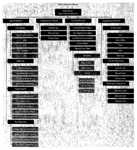
[0009] Figure 1: This figure describes the overall architecture of the radar
system. The interconnection between the major components of the C4I
infrastructure, are
interlaced within the sensor network. This figure represents the high level
architecture of
the system, i.e., the global level, and comprises the integrated command,
control,
communication and computation networks and the C4I infrastructure. The
communication infrastructure can take the form of all conventional and future
communication schemes including wired, wireless, optical, RF etc.
[0010] Figure 2: This figure represents the organization and implementation
of the functional modality of the radar. Inputs from the individual parts of
the radar as an
example of a generic sensor are used to calculate the output requirements of
the sensor.
In this fashion, the radar (sensor) operational configuration is synthesized
using an
appropriate processor and software. Changes in sensor modality are
incorporated by
modifying software and sensor inputs. Communication, control, command and
1797328.01
-4-
CA 02527210 2005-11-24
WO 2004/106965 PCT/US2004/016762
computational interfaces are similar, i.e., analogous, to those of Figure 1
(this is called
the concept of self similarity). The overall architecture is consistent by
self similarity
with the other (subordinate) levels in that it comprises communication
channels
connecting computational, memory, control, and infrastructure networks
(subunits such
as modules or devices) to produce functionality.
[0011] Figure 3: This figure represents a lower level in the overall
architecture of the radar (sensor) system. This level provides integration of
several
individual components that make up typical radar (sensor) systems (e.g.,
individual
antenna elements, etc). This device integration configures individual inputs
or outputs of
the system that are used to form the input to the mid level architecture
(described in
Figure 2). Components include computational, storage, memory, command,
control, and
communications infrastructure in a manner similar to the previously described
levels.
[0012] Figure 4: This figure describes the architecture of individual
components of the sensor system. The components are implemented using
computational
devices and software. The functional behavior of the components can be changed
by
reprogramming the computational devices. This capability is illustrated by
describing the
architecture of a pulse modulator network, however, this approach is
applicable to all
component level devices with the sensor architecture.
[0013] Figure 5: This figure illustrates a high performance optical ADC.
[0014] Figure 6: This figure illustrates a front end of a generalized RF.
[0015] Figure 7: This figure illustrates a functional block diagram.
[0016] Figure 8: This figure illustrates a network receiver front end version
1
[0017] Figure 9: This figure illustrates a network receiver front end version
2.
[0018] Figure 10: This figure illustrates two versions of the AGC control
implementation.
[0019] Figure 11: This figure illustrates a pulse former module.
[0020] Figure 12: This figure illustrates an upper level system architecture.
1797328.01
-5-
CA 02527210 2005-11-24
WO 2004/106965 PCT/US2004/016762
[0021] Figure 13: This figure illustrates the system command interfaces.
[0022] Figure 14: This figure illustrates the system control interfaces.
[0023] Figure 15: This figure illustrates the computational architecture of
the
upper level
architecture.
[0024] Figure This figure illustrates the system communications
16: interface.
[0025] Figure This figure illustrates the mid level
17: system architecture.
[0026] Figure This figure illustrates a mid level functional
18: block diagram.
[0027] Figure This figure illustrates the beam former
19: architecture.
[0028] Figure This figure illustrates the Doppler processor
20: architecture.
[0029] Figure This figure illustrates the range gate
21: processor architecture.
[0030] Figure This figure illustrates clutter canceller
22: architecture/
[0031] Figure This figure illustrates lower level system
23: architecture.
[0032] Figure This figure illustrates the functional
24: requirements of the
lower level system architecture.
[0033] The invention and objects and features thereof will be more readily
apparent from the following detailed description and appended claims when
taken with
the drawings. The component level architecture will have the same general
organizational structure as the higher level components of the system
architecture.
Networlc, storage, memory, computational, communication and control components
are
all represented, with the addition of analog interfaces for analog (in the
specific case of
the RADAR RF) inputs and outputs. Key representations illustrate the
hierarchical
nature of the system design and architectural siTlxcture. Although components
are critical
to overall implementation, the architectural structure allows flexibility in
achievable
performance, scalability for future performance improvements and resilient
design
minimizing architectural changes in future system implementations.
[0034] As a specific example we describe the elements of a RADAR system,
however these concepts are applicable to any sensor or communication system
where
1797328.01
-6-
CA 02527210 2005-11-24
WO 2004/106965 PCT/US2004/016762
these methodologies have appropriateness. Major components critical to the RF
front-
end implementation include, ADC modules, RF front end modules, AGC modules,
LNA
modules, and pulse modulator/demodulator modules. Each of the component
modules
are described in the following paragraphs and illustrate the concepts
described in detail in
the following paragraphs.
DETAILED DESCRIPTION OF THE INVENTION
[0035] Figure 1 illustrates the upper level architecture. It is in this level
that
system configuration and operational mode is most generally defined and
managed.
Typically the infrastructure supports the global interfaces of the overall
system for
external system clients, e.g., providing intelligence, surveillance, and
reconnaissance
(ISR) data products to network centric users or clients for battlefield
management.
Bandwidth requirements at a given level or in communication with layers above
or below
may span the range of very low to extremely high. Generally, system control
requirements tend to utilize low bandwidth and information or data transport
require high
bandwidth conduits. The network components are inherently distributed.
Computation
components will not reside only in one location, and in some case may be
distributed
with sensor components as well as computational engines localized at command
central.
The approach configures resources to optimize functional requirements,
information
generation, information transfer, system control and configuration, and the
allocation of
communication resources based on Quality of Service (QoS) requirements and
hierarchy.
This particular infrastructure will utilize current and future generations of
communication
interfaces such as distributed fixed based wireless systems, 3 and 4 G
wireless constructs,
optical and legacy wired infrastructures, etc.
[0036] The midlevel architecture is shown in Figure 2. This level of the
system describes system functionality rather than configuration. In the
example shown in
the figure, the I/O infrastructure is represented as 'input' and parallel
outputs to the
'SAR, MTI, Traclc, etc. processor'. Control, communication, and processor are
shown
integrated with a SAN, and the processor is coupled to subunits that comprise
specific
functional modules at the next lower level.
1797328.01
_7_
CA 02527210 2005-11-24
WO 2004/106965 PCT/US2004/016762
[0037] Once the incoming signal has been digitized, a network of distributed
communication and processing hardware and software produces the required
transformations. Since this portion of the architecture is mostly
communication and
processor driven, progressive system upgrades can be included in the
architecture design.
Requirements at this level may include reconfigurability, resiliency,
distributed
computational interfaces, computational redundancy and self
organization/healing. This
architectural level will have interfaces to the upper level and lower level
architectural
structure. C4I interfaces will include traditional low bandwidth conduits and
extremely
high bandwidth infrastructure typically at the interface to hardware
processors that axe
required to implement functionality.
[0038] The next level of architecture is the lower level shown in Figure 3.
This level may comprise the set of functional modules. The integration of
device,
communication and computational resources are included in this lower level
descriptor.
This level is dominated by high band width communication interfaces that
support both
processor functionality and communication interfaces. This connectivity takes
the form
of conventional communications architecture as well as buss-oriented
architectures
associated with memory and storage interfaces. In some cases, memory and
computational resources axe shared between devices, communications interfaces
and
computational structures. This level specifies the fusion between compute,
cornlnunicate
and the individual devices that make up higher level components (e.g.
automatic gain
control: AGC's, low noise amplifiers: LNA's, analog-digital converters: ADC's,
etc.).
Each antenna element has a transceiver pair that is constructed from
individual
components each of which have compute, communicate and control structures.
[0039] The device structures are described as block diagrams in Figure 4.
Shown is an example of advanced integrated devices that share a common C4I
architecture. The upper diagram represents the analog hardware for a pulse
modulator,
the middle diagram is a functional block diagram for a 'software' pulse
modulator, and
the lower diagram is the pulse modulator network implementation in the self
similar
hierarchical scheme. In analog radars, the pulse shaper is a hardware-
implemented
device with limited flexibility. In the example, the pulse shape is tied to
the surface
acoustic wave (SAW) device. The output signal is dictated by the set of design
1797328.01
_8_
CA 02527210 2005-11-24
WO 2004/106965 PCT/US2004/016762
specifications describing the overall structure. System flexibility is
severely limited
because of the hardware implementation. Because pulse shape cannot be altered
without
changing the SAW device, mufti modal functionality of the system is
compromised.
[0040] More generalized and adaptable function is realized in the 'software
embodied' Pulse Shaper device that is illustrated in the middle section of
Figure 4.
Specific output pulse shapes can be realized using lookup tables and mixer
functions.
Aliased time domain signals can be effectively reduced using filters that are
either
digitally generated or implemented in real time. A hardware-implemented filter
must be
tunable and have sufficient RF and control bandwidth (pulse to pulse tunable
time
constant) to provide adequate blanking of the output RF pulse stream. This
functional
scheme allows waveform selectivity, mufti-modal system performance, and
calibration
control, to be implemented within the same system architecture.
[0041] A more effective architecture implements the entire pulse shaping
process in software. Pulse shape, mixing functions, alias filters can be
individually
controlled. This approach allows multifunction capability, mufti-modal
behavior, all on a
pulse-to-pulse timing scheme. In this manner, adaptable system perforW ance is
achieved.
[0042] The hierarchical scheme may be realized in the design of a radar or
sensor system by the following steps:
(1) identifying a global system organizational layer or level that comprises a
structure that includes command, control, communication, and computational or
processor elements,
(2) identifying at least one subordinate organizational layer or level that
has
analogous elements to the global system layer,
(3) defining and assigning C4I functional processes and configuration or
performance characteristics for each level, and
(4) defining and specifying interface requirements between each neighboring
level.
[0043] The ADC modules are the most critical to defining overall digital
system performance. System bandwidth, sample rate, resolution, and operational
1797328.01
-9-
CA 02527210 2005-11-24
WO 2004/106965 PCT/US2004/016762
frequency all qualify the balance of the system implementation. The design
illustrated in
Figure 5 is based on the high performance component of the future. With a 50
GHz
potential sample rate this device could be used to sample base band
frequencies up to 25
GHz. With the bandwidth of the RF signal approaching 100 to 250 MHz, this
would
provide a 10 to 25 times over-sampling potential. If available ADCs have less
sampling
capability, several alternatives will be used to move the digital conversion
process as near
to the RF front end as possible. Key to this implementation is the chosen
architecture of
the concept. Potential implementation strategies are illustrated in the next
sections.
[0044] A generalized RF frontend is illustrated in Figure 6. THE STALO and
COHO are included to provide down conversion to a frequency range where video
processing can be implemented (both bandwidth and central frequency of the
processor
components). The functional behavior of this processing stream is illustrated
in Figure 7
[19]. If the ADCs used are incapable of sampling base-band frequencies, the
reference
clocks are chosen to allow frequencies within the performance specifications
of the
ADCs. This architecture will allow continuous system upgrade as ADC
performance
improves, without major system redesign.
[0045] Critical components of the system front end are the mixers and LNAs.
The low noise amplifier sets the noise performance of the entire front end of
the system.
Any components such as filters or switches before the LNA will negatively
impact the
noise figure of the system if they exhibit loss or non linearity. HTS and
cooled
components can help to minimize this effect. Typical implementation approaches
are
illustrated in the next section.
[0046] Figure 8 illustrates a hybrid architecture that allows some down
conversion capability at the system front end to match to the sampling
characteristics of
the ADC. The two frequencies can be coherently generated from a single master
clock.
This allows coherent timing of sample points, offsets, sample and hold
functions, a fixed
reference between I and Q channels and referenced inter-module sampling. As
ADC
performance improves all of these functional requirements continue to exist
without
redesign or modification. When ADC sampling rates allow base-band conversion
the
mixer functional can be eliminated from the system. This is illustrated in
Figure 9.
1797328.01
-10-
CA 02527210 2005-11-24
WO 2004/106965 PCT/US2004/016762
[0047] As soon as the signal reaches the ADC the balance of the signal paths
consist of network interfaces. These are designated by the red component
interfaces.
The processor provides computational resources for signal conditioning,
component
control signals, I/O interfaces and communication interface to the balance of
the system
infrastructure. The networlc interface between the processor and the memory
will likely
be optimized to provide for transfer characteristics dictated by the
processor. Other
network physical layer and control layer protocols are more conventional in
nature.
Since the concept uses a hierarchical architecture, individual components
typically
associated with the receiver front end also have a network-based architecture.
This is
illustrated in the next section using the LNA/AGC component as a typical
example.
[0048] Figure 10 illustrates two concepts of a typical AGC loop. The more
traditional approach is described by the upper block diagram [19]. The RF
signal is
detected using a square law detector, sampled at low sample rate ADC analyzed
by the
processor and moved to a buffer. The output of the buffer is converted to
analog and
used to modify the gain of a voltage controlled LNA. The output RF out #1 is
then used
as the RF input to the balance of the RF front end. The lower block diagram in
Figure 10
illustrated a more advanced implementation where the sampling rate of the ADC
is high
enough to produce digital RF at out put 2. The AGC processing is performed on
the high
rate sampled signal using the processor to low pass filter and generate the
AGC control
signal to the LNA. Either version is allowable and can be scaled to
incorporate improved
performance devices.
[0049] One of the most critical design components of the radar front end is
the output pulse former. Specification of this subsystem impact SNR, clutter
rejection,
system gain, incorporated bandwidth, radiated power, and system response.
Unfortunately, traditional systems commit the design to hardware
implementation and
eliminate signal shape selection and modulation/demodulation flexibility. This
architecture strategy allows flexible shape selection, flexible
demodulation/modulation
scheme, and modality selection to be easily incorporated. The approach is
illustrated in
Figure 11. This particular approach mimics the software and digital radio
schemes
currently used in commercial telecommunication infrastructure. Documented
benefits
include lower power requirements, improved SNR, higher quality signal
structure, and
1797328.01
-11-
CA 02527210 2005-11-24
WO 2004/106965 PCT/US2004/016762
increased allowable bandwidth. These technologies are directly transferable to
radar and
sensor architectures.
[0050] The conceptual design is described as a hierarchal description of four
levels. The upper level is characterized by C4I descriptors integrated by wide
area
networlcing infrastructure. The midlevel descriptor is characterized by global
system
functionality integrated by more metro areas network computational interfaces.
The
lower level descriptor is characterized by subsystem physical connectivity
integrated with
local area network connectivity. The final layer (component layer) is
characterized by
descriptors of individual functional components suppouted by pico-networlc
interfaces.
This hierarchal structure is used to facilitate flexibility, upgrade without
redesign,
reconfigurability, mufti-modal operation, resiliency, and redundancy. Each
module can
be described by a set of parameters with upper ands lower bounds. Once these
have been
identified, implementation schemes can be identified, and configuration down
select
initiated. The preliminary design process can then be started.
[0051] The upper level organizational diagram is illustrated in Figure 12. The
major interfaces of this organizational map include the traditional C4I
interfaces.
Battlefield management interfaces will be supported by traditional and
advanced
communications infrastructure. Within the sensor communication environment,
sensor
interfaces will include Control network interfaces, Communication networlc
interfaces,
Command networlc interfaces and Computational networlc interfaces. Control
interfaces
will accommodate system functional mode, system calibration, system health
assessment,
system reconfiguration, navigation interfaces, and system power management
control.
Communication interfaces will accommodate the physical, control and protocol
layers
associated with traditional communication lincs. This communication link is
primarily
concerned with data transfer.
[0052] The command interface supports internal data assimilation and
analysis, battlefield management issues, and quality of service prioritization
and
implementation. Command access may be though any one of the four modules and
direct
interfaces can exist between each of the modules accessible though command
GUIs or
any of the modules individually or collectively. Finally, the computational
interfaces
1797328.01
-12-
CA 02527210 2005-11-24
WO 2004/106965 PCT/US2004/016762
support, both internal and external data analysis, information generation,
product
generation, and computational requirements associated with battlefield
management
decision malting. The conceptual design requirements of each of the upper
level system
modules will be describe in the following sections.
[0053] The functional interfaces of the Command Architecture are illustrated
in Figure 13. Critical issues include the requirement to task sensor
performance and
modality, monitor external C4I interfaces, and task communication and
computational
resources.
[0054] The Command Architecture will have the following functional support
infrastructure:
~ Local Infrastructure network management
~ QoS requirements management
~ Protocol infrastructure management
~ External network interface management
~ Physical layer management (including wireless and wired interfaces)
~ Control layer management
~ Interface to local and global Communications, Control and Computational
support
infrastructure
[0055] Performance requirements of the Command Architecture will be
specific to the operation of the sensors and their interface to command
infrastructure.
~ Local Infrastructure network management
o Support bandwidth sufficient to task sensors (low data rate sensor control
commands 10's of I~bps, high data rate calibration parameters, targeting
data, etc. >lOGbps
o Low latency (less that 1 second )
o Reconfigurable within 1 second
o QoS command interfaces (C4I local and global connectivity, redundancy,
reconfigurability, low to high data rates, kbps to gbps capable)
~ QoS requirements management
o Architecture has organization control of QoS protocol selection and
implementation.
1797328.01
-13-
CA 02527210 2005-11-24
WO 2004/106965 PCT/US2004/016762
o Override control of Asset functionality, operation configuration and
pointing
o Low bandwidth (~lcbps) commmlication interfaces enabled by point and
cliclc functionality.
~ Protocol infrastructure management
o Pre-determined protocol selection stack
o Provision for online modification of protocol stack as situations permit
o Embedded priority selection
o Selectable variable communication and control architecture
~ External network interface management
o Management of external communication interfaces
o Selection of data formats (automated)
o Selection of encryption algorithms (automated)
o Selection of the commmlication physical layer (manual <1 sec, automated
<1 OOms)
o Generation of interface protocols (automatic)
o Command of system override functionality (<1 sec)
~ Physical layer management (including wireless and wired interfaces)
o Automated physical interconnect selection (switchover <1 sec)
o Redundancy and reconfigurability management (automated, switch
latency < 100 ms)
o Traffic provisioning
~ Interface to local and global Communications, Control and Computational
support
infrastructure
o GUI interface
o Seamless interconnect to communications, control and computational
networks
o GUI bandwidth required to support display, control, and command
functions (e.g. image refresh ~XVGA at 30 fps)
1797328.01
-14-
CA 02527210 2005-11-24
WO 2004/106965 PCT/US2004/016762
The design constrains focus on the ability to improve system performance,
allow
performance upgrades and incorporate revolutionary system design
implementations.
The main elements are listed below:
~ Minimize power consumption
~ Open architecture
~ Upgrade potential for the future
~ Short term dem-val capability
~ Long term integration and procurement
~ Reduced concept to deployment timeline
~ TULIP conforming protocol
~ Direct interface to DoD- Tactical Common Data Linlc
[0056] The major interfaces of the sensor control architecture are illustrated
in
Figure 14. Functional interfaces will vary from level to level as appropriate.
[0057] The major functional requirements of the control architecture are
listed
as follows:
~ Command system functionality (including Beam Scan/formation, ECM,
MTI, Imaging, PPI, etc.)
~ Command system calibration (including phase, amplitude, system
nonlinearity, polarization, etc.)
~ Monitor and control system health (including, thermal management,
output power, system noise figure, cal point drift, end to end system
performance, etc.)
~ Control system reconfiguration (including, component loss assessment,
auxiliary component injection, system reconfiguration, graceful
degradation, etc.)
[0058] Performance requirements of the Control Architecture will be specific
to the operation of the sensors and their interface to command infrastructure.
~ Monitor and control system functionality
1797328.01
-15-
CA 02527210 2005-11-24
WO 2004/106965 PCT/US2004/016762
o Support bandwidth sufficient to task sensors (low data rate sensor control
commands 10's of Kbps, high data rate calibration parameters, targeting
data, etc. >lOGbps )
o Low latency (less that 1 second )
o Reconfigurable within 1 second
o Download specialty performance characteristics e.g. new wave forms,
processing parameters, etc. (C4I local and global connectivity,
redundancy, low to high data rates, Kbps to Gbps capable)
o Integrate navigation (INS and GPS) inputs to system control requirements
(support communication bandwidth necessary for system functionality,
requirements dictated by the implemented navigation architecture). For
example a closely coupled INS/GPS requires shoat interval updates from
GPS (higher bandwidth requirements). Loosely coupled systems can rely
on the INS to provide short interval navigation information with longer
interval correction from GPS downloads (lower bandwidth requirements).
~ Monitor and control system calibration
o Architecture has organization control of calibration at the component, low
and mid level system architecture points
o Override control of Asset functionality, operation configuration and
pointing
o Low bandwidth (~lcbps) communication interfaces support by high band
with communication ports when required.
~ Monitor and control system health
o Collect sensor measurement data assess conditions (~Kbps comm.
interfaces)
o Provision for online system heal assessment and performance
o Embedded redundancy selection
o Selectable variable communication and control architecture interfaces
~ Monitor and control system reconfiguration
o Management of external system assessment interfaces
o Selection of system reconfiguration (automated)
1797328.01
-16-
CA 02527210 2005-11-24
WO 2004/106965 PCT/US2004/016762
o selection of performance modes (manual)
o Generation of graceful degradation protocols (automatic)
o Command of system override functionality (<1 sec)
The design constrains focus on the ability to improve system performance,
allow
performance upgrades and incorporate revolutionary system design
implementations.
The main elements are listed below:
~ Minimize power consumption
~ Open architecture
~ Upgrade potential for the future
~ Short term dem-val capability
~ Long term integration and procurement
~ Reduced concept to deployment timeline
~ TULIP conforming protocol
~ Direct interface to DoD- Tactical Common Data Link
~ Selection of minimum performance specifications
[0059] The computational architecture of the upper level architecture is
illustrated in Figure 15. One of the most critical functional requirements is
scalable
performance capability. The particular architecture presumes a parallel
computational
interface. Most computational functions in the upper level architecture are
inherently
parallel. This approach will allow scalable processing power upgrades will
little system
redesign. The design approach allow all types of compute clusters as well,
including
microprocessors, Field Prograanmable Gate Arrays (FPGAs), DSPs, ASICs, and any
other current or yet to be developed technologies.
[0060] The maj or functional requirements of the computational
architecture are listed as follows:
~ Support the I/O interface in the C4I infrastructure including text, multi-
media, video, real time product generation, etc.
1797328.01
-17-
CA 02527210 2005-11-24
WO 2004/106965 PCT/US2004/016762
~ Support internal communication protocols (between processors and within
the LAN and WAN of the C4I infrastructure.
~ Support information generation from multiple sensor, data base and
communication inputs.
~ Support automated information analysis
~ Support the GUI to the C4I infrastructure.
[0061] Performance requirements of the Computational Architecture will
be specific to the operation of the sensors and their interface to command
infrastructure.
~ Support the I/O interface in the C4I infrastructure including text, multi-
media, video, real time product generation, etc.
o computational speed will vary from l Os of GFLOPs per seconds
for a single computational processor, to greater than a TFLOPs per
second for multi processor functionality
o Low latency (less that 1 second)
o Reconfigurable within 1 second
o Hot swappable hardware
~ Support internal communication protocols (between processors and within
the LAN and WAN of the C4I infrastructure.
o (Inter-device communication and data transfer bandwidths will
approach 350 to 500 MBps.
o LAN and WAN bandwidths will require 10 to 40 Gbps for
adequate data and information transfer).
~ Support information generation from multiple sensor, data base and
communication inputs.
o computational speed will vary from l Os of GFLOPs per seconds
for a single computational processor, to greater than a TFLOPs per
second for mufti processor functionality
1797328.01
-18-
CA 02527210 2005-11-24
WO 2004/106965 PCT/US2004/016762
o Memory requirements vary from one giga-byte per individual
processor to greater than a terabyte for the aggregate
computational system
o Memory speeds support processor requirements
o Memory buss structure specific to processor architecture
o Storage requirements structure on a enterprise oriented, fiber
interfaced Storage Area Network (SAN) (total storage capacity on
the order of 1 OOs of terra-bytes)
~ Support automated information analysis
o Meet the needs of the C4I infrastructure (real time, latency,
quality, etc.)
~ Support the GUI to the C4I infrastructure.
o Meet the needs of the C4I command infrastructure
[0062] The design constraints focus on the ability to improve system
performance, allow performance upgrades and incorporate revolutionary system
design
implementations. The main elements are listed below:
~ Minimize power consumption
~ Open architecture
~ Upgrade potential for the future
~ Short term dem-val capability
~ Long term integration and procurement
~ Reduced concept to deployment timeline
~ TULIP conforming protocol
~ Direct interface to DoD- Tactical Common Data Link
~ Scalable architecture
[0063] The communication architecture of the upper level architecture is
illustrated in Figure 16. One of the most critical functional requirements is
scalable and
interoperable infrastructure.
1797328.01
-19-
CA 02527210 2005-11-24
WO 2004/106965 PCT/US2004/016762
1UU641 l he major hinctional requirements of the computational architecture
are listed as follows:
~ Support the communications I/O interface in the C4I infrastructure
including text, mufti-media, video, real time product generation, etc.
~ Support internal communication protocols (between processors and within
the LAN and WAN of the C4I infrastructure.
~ Support information transfer from multiple sensor, data base and C4I
inputs.
~ Support automated information analysis
~ Support the communications requirements to the~GUI and the C4I
infrastructure.
~ Support the Control, physical and protocol layers of the communications
infrastructure
Performance Requirements
[0065] Perfoi~rnance requirements of the Computational Architecture will be
specific to the operation of the sensors and their interface to command
infrastructure.
~ Support the communications I/O interface in the C4I infrastructure
including text, mufti-media, video, real time product generation, etc.
~ Support internal communication protocols (between processors and within
the LAN and WAN of the C4I infrastructure.
o Support QoS protocols
o Support physical and control communication infrastructure
(typically lcbps, to fractional gbps interfaces)
~ Support information transfer from multiple sensor, data base and C4I
inputs.
o Support lcbps to gbps interfaces
1797328.01
-20-
CA 02527210 2005-11-24
WO 2004/106965 PCT/US2004/016762
~ support the communications requirements to the GUI and the C4I
infrastructure.
o Support mbps to gbps bandwidths
~ Support the control, physical and protocol layers of the communications
infrastructure
o Support gbps bandwidths, interoperability, multiple physical layers
and multiple protocols
[0066] The design constrains focus on the ability to improve system
performance, allow performance upgrades and incorporate revolutionary system
design
implementations. The main elements axe listed below:
~ Minimize power consumption
~ Open architecture
~ Upgrade potential for the future
~ Short term dem-val capability
~ Long term integration and procurement
~ Reduced concept to deployment timeline
~ TULIP conforming protocol
~ Direct interface to DoD- Tactical Common Data Linlc
~ Scalable architecture
[0067] The objective of the midlevel architecture is to support the
computational functionality of the sensor system. This component of the
systems
architecture is where both hardware and software interfaces are constructed
and managed.
The mid level architecture modules are illustrated in Figure 17. The software
implement
models include the beam former, clutter canceller, Doppler filters, and range
gate filters.
The hardware implementation infrastructure comprises the SAN, Memory,
Processors,
and communication infrastructure. Functionally this architectural level
provides the
sensor with modality selection under software control and interface to the
upper level
architecture. Block diagram functionality is illustrated in Figure 1 S.
1797328.01
-21 -
CA 02527210 2005-11-24
WO 2004/106965 PCT/US2004/016762
[0068] The major components of the mid level architecture include the
following:
~ Beam Former:
o Processor
o Calibration Loop
o Implementation algorithm
o Memory
o Storage
o I/O interfaces
~ Doppler filters
o Processor
o Calibration Loop
o Implementation algorithm
o Memory
o Storage
o I/O interfaces
0
~ Range Gate filters
o Processor
o Calibration Loop
o Implementation algorithm
o Memory
o Storage
o I/O interfaces
0
~ Clutter canceller
o Processor
o Calibration Loop
o Implementation algorithm
o Memory
o Storage
1797328.01
-22-
CA 02527210 2005-11-24
WO 2004/106965 PCT/US2004/016762
o iiu mtertaces
0
~ SAN
o Storage layer
o Switch/router layer
o Processorlayer
o I/O interface
o Memory
~ Memory
o Local
o Distributed
o Data Buss
o Communications interface
~ Processors
o Local
o Distributed
o Global
o Memory
o Storage
o Communications interface
~ Communications Infrastructure
o Physical Layer
o Protocol Layer
o Control Layer
[0069] The beam former implementation scheme is illustrated in Figure 19.
[0070] The major data structures for this mid level architecture include the
following:
~ Input data structure from the lower level architecture modules (Quadrature
digital
data from the output of the antenna elements (12 to 16 bit ADC output, 64 bit
floating point, time stamp, format compatible with the optical input of the
SAN))
1797328.01
- 23 -
CA 02527210 2005-11-24
WO 2004/106965 PCT/US2004/016762
~ Output data from the SAN to the processors (format compatible with the
output of
the SAN, input of the processor, Memory interface specific to the buss
structure
of the processor, processor output format compatible with the specified
network
protocol (variable)) Processor interface structure is illustrated in Figure
14).
~ Communication data structures compatible with network physical layer,
control
layer, and protocol layer requirements.
~ Navigation Data structure from GPS/INS, compatible with output of both
devices
[0071] The major external interfaces to the beam former module include:
~ Data interface to sensor front end
~ Data interface to sensor modality processors
~ Data interface to the C4I infrastructure
~ Data interface to Navigation system
[0072] The major internal interfaces of the beam former module include the
following:
~ Memory
~ Storage
~ Multiprocessor
~ Control
~ Communication
~ Network
[0073] Critical to future scalability issues is the incorporation of a
networked
infrastructure in all module components. The SAN, Processor, memory and C4I
interfaces require mufti module architectures to be expandable. Although a
single
module SAN could be incorporated in a design, it is understood that this would
be
implemented with multiple SAN's on the same network with access to several
processor
module functions. The inherent assumption of networked architectures for ADC,
memory, storage, network and processor components enable future upgrade and
scalable
performance improvements without system redesign. Design architectures that
inherently
rely on a single device to implement functionality have restricted upgrade
capability.
Functionality is limited by device specification and performance, upgraded
performance
1797328.01
-24-
CA 02527210 2005-11-24
WO 2004/106965 PCT/US2004/016762
reqmres devices with improved capability generally requiring redesigned
architectures.
The suggested architecture assumes networlced interfaces that accommodate
multiple
devices, each sharing performance requirements. When improved functionality is
required, additional devices can be added to the network architecture without
the need for
redesign. The architecture accommodates improved functionality, and transition
from
analog to digital (and vice versa) within its original structure.
[0074] Very few technical risks exist with this architecture design. Limited
performance item need only be placed in parallel to achieve performance gains.
Tradeoff
with footprint, power consumption, etc. will force transition solutions to be
implemented.
Within the foreseeable future, technical performance will not be limited by
device
governing laws.
[0075] The beam former implementation scheme is illustrated in Figure 20.
[0076] The major data structures for this mid level architecture are similar
to
the beam former and include the following:
~ Input data structure from the lower level architecture modules (Quadrature
digital data from the output of the antenna elements (12 to 16 bit ADC out
put,
64 bit floating point, time stamp, format compatible with the optical input of
the
SAN))
~ Output data from the SAN to the processors (format compatible with the
output
of the SAN, input of the processor, Memory interface specific to the buss
structure of the processor, processor output format compatible with the
specified
network protocol (variable)) Processor interface structure is illustrated in
Figure 53)
~ Communication data structures compatible with networlc physical layer,
control
layer, and protocol layer requirements.
~ Navigation Data structure from GPS/1NS, compatible with output of both
devices
[0077] The major external interfaces to the beam former module include:
~ Data interface to sensor front end
1797328.01
- 25 -
CA 02527210 2005-11-24
WO 2004/106965 PCT/US2004/016762
~ Data interface to sensor modality processors
~ Data interface to the C4I infrastructure
~ Data interface to Navigation system
[0078] The major internal interfaces of the beam former module include the
following:
~ Memory
~ Storage
~ Multiprocessor
~ Control
~ Communication
~ Network
1797328.01
-26-
CA 02527210 2005-11-24
WO 2004/106965 PCT/US2004/016762
luuryl critical to future scalability issues is the incorporation of parallel
infrastructure in all module components. The SAN, Processor, memory and C4I
interfaces require multi module architectures to be expandable. Although a
single
module SAN can be used, it is understood that this would be implemented with
multiple
SAN's on the same network with access to several processor module functions.
The
inherent assumption of parallel architectures for ADC, memory, storage,
network and
processor components enables future upgrade and scalable performance
improvements
without system redesign.
[0080] Very few technical risks exist with this architecture design. Limited
performance item need only be placed in parallel to achieve performance gains.
Tradeoff
with footprint, power consumption, etc. will force transition solutions to be
implemented.
Within the foreseeable future technical performance will not be limited by
device
governing laws.
Range Gating function
[0081] The range gate implementation scheme is illustrated in Figure 21.
[0082] The major data structures for this mid level architecture are similar
to
the range gate processor and include the following:
~ Input data structure from the lower level architecture modules (Quadrature
digital
data from the output of the antenna elements (12 to 16 bit ADC out put, 64 bit
floating point, time stamp, format compatible with the optical input of the
SAN))
~ Output data from the SAN to the processors (format compatible with the
output of
the SAN, input of the processor, Memory interface specific to the buss
structure
of the processor, processor output format compatible with the specified
networlc
protocol (variable)) Processor interface structure is illustrated in Figure
53)
~ Communication data structures compatible with network physical layer,
control
layer, and protocol layer requirements.
~ Navigation Data structure from GPS/INS, compatible with output of both
devices
1797328.01
-27-
CA 02527210 2005-11-24
WO 2004/106965 PCT/US2004/016762
luu~s~l i ne mayor external interfaces to the beam former module include:
~ Data interface to sensor front end
~ Data interface to sensor modality processors
~ Data interface to the C4I infrastructure
~ Data interface to Navigation system
[0084] The major internal interfaces of the beam former module include the
following:
~ Memory
~ Storage
~ Multiprocessor
~ Control
~ Communication
~ Network
[0085] Critical to future scalability issues is the incorporation of parallel
infrastructure in all module components. The SAN, Processor, memory and C4I
interfaces require multi module architectures to be expandable. The inherent
assumption
of parallel architectures for ADC, memory, storage, network and processor
components
enables future upgrade and scalable performance improvements without system
redesign.
[0086] Very few technical risks exist with this architecture design. Limited
performance item need only be placed in parallel to achieve performance gains.
Tradeoff
with footprint, power consumption, etc. will force transition solutions to be
implemented.
Within the foreseeable future technical performance will not be limited by
device
governing laws.
Clutter Canceller Function
1797328.01
CA 02527210 2005-11-24
WO 2004/106965 PCT/US2004/016762
~ me cm~er processor implementation scheme is illustrated in Figure
22.
[0088] The major data structures for this mid level architecture are similar
to
the clutter canceller processor and include the following:
~ Input data structure from the lower level architecture modules (Quadrature
digital
data from the output of the antenna elements (12 to 16 bit ADC out put, 64 bit
floating point, time stamp, format compatible with the optical input of the
SAN))
~ Output data from the SAN to the processors (format compatible with the
output of
the SAN, input of the processor, Memory interface specific to the buss
structure
of the processor, processor output format compatible with the specified
network
protocol (variable)) Processor interface structure is illustrated in Figure
53)
~ Communication data structures compatible with network physical layer,
control
layer, and protocol layer requirements.
~ Navigation Data structure from GPS/INS, compatible with output of both
devices
[0089] The major external interfaces to the beam former module include:
~ Data interface to sensor front end
~ Data interface to sensor modality processors
~ Data interface to the C4I infrastructure
~ Data interface to Navigation system
[0090] The major internal interfaces of the beam former module include the
following:
~ Memory
~ Storage
~ Multiprocessor
~ Control
~ Communication
~ Network
[0091] Critical to future scalability issues is the incorporation of paxallel
infrastructure in all module components. The SAN, Processor, memory and C4I
1797328.01
-29-
CA 02527210 2005-11-24
WO 2004/106965 PCT/US2004/016762
mtertaces require mufti module architectures to be expandable. The inherent
assumption
of parallel architectures for ADC, memory, storage, networlc and processor
components
enables future upgrade and scalable performance improvements without system
redesign.
[0092] SAN Infrastructure, Memory, Network Infrastructure, Processor,
Communications Infrastructure
[0093] The major data structures for these mid level architecture are similar
and include the following:
~ I/O data structure
~ Control data structures
~ Cormnunication data structures compatible with network physical layer,
control
layer, and protocol layer requirements.
[0094] The major external interfaces to the beam former module include:
~ Data interface to sensor front end
~ Data interface to sensor modality processors
~ Data interface to the C4I infrastructure
~ Data interface to Navigation system
[0095] The major internal interfaces of the beam former module include the
following:
~ Memory
~ Storage
~ Multiprocessor
~ Control
~ Communication
~ Network
[0096] Critical to future scalability issues is the incorporation of parallel
infrastructure in all module components. The SAN, Processor, memory and C4I
interfaces require mufti-module architectures to be expandable. It is
understood that
these would be implemented with multiple devices on the same networlc with
access to
1797328.01
-30-
CA 02527210 2005-11-24
WO 2004/106965 PCT/US2004/016762
several processor module functions. The inherent assumption of parallel
architectures for
ADC, memory, storage, networlc and processor components enables future upgrade
and
scalable performance improvements without system redesign.
[0097] Lower level system architecture describes the fusion of hardware and
software components just above the individual component level. The lower level
architecture is illustrated in Figure 23. Typical lower level subsystems are
constructed
with individual devices, network interfaces, communication interfaces,
computational
components, and calibration infrastructure. This layer represents the fusion
of hardware
components, computational resources, calibration approaches, and any
preprocessing
required to precondition signals for subsequent operations. A functional block
diagram
of the lower level architecture is illustrated in Figure 24. The diagram
represents the
integration of multiple components within the system. A typical example (but
not the
sole case) is the integration of individual elements of the transceiver
structure. Each of
the radiation elements (including front end, mixers, calibration units, ADC's,
etc) are
connected to processing, calibration, memory or storage elements and
external/internal
communication infrastructure. The individual components of the process are
described in
the next sections.
[0098] Calibration processes are incorporated throughout the system
architecture [19, 20]. Processes are integrated at the appropriate level with
in the system
to fulfill correction of non-linearity within components, subsystems, and/or
overall
system transfer functions. All will have interfaces to communication network,
access to
processor and memory functionality, and interface to C4I infrastructure. The
example
describes the cross element normalization necessary for the beam forming or
steering
process. Internal calibration cycles and injection points will occur within
elements, within
components that comprise elements and at processing points external to the
lower level
system architecture.
[0099] The preprocessing functionality supports a number of signal
conditioning requirements throughout the lower level architecture. These
include signal
conditioning functions (e.g. averaging, noise reduction, estimation, signal
statistics, etc.),
timing and phase corrections, normalization with the element, as well as
across elements,
1797328.01
-31-
CA 02527210 2005-11-24
WO 2004/106965 PCT/US2004/016762
signal routing, storage and memory management, communication and control
interfaces,
and I/O interface management. Preprocessing functionality tend to support
element and
component signal processing requirements within components and within element
subsystems. Such systems are, dedicated to a specific task, interface to local
element
networlcs, respond to limited external control functions, require high
computational
throughput (e.g. FFT and DSP computational speeds on a pulse to pulse time
scale [20,
21].) and consequently are specified with high computational speeds, large
local memory
and relatively high network bandwidths.
[00100] The computational fusion functionality typically takes place external
to the element layer with in the lower level system architecture.
Computational
requirements typically are supported by more genera purpose processors. These
computational units are design to integrate all of the computational
requirements on
individual parallel element subsystems. Within element processing
functionality, as well
as external element processing requirements are managed at this level. Shared
memory,
shared storage and shared network and communication functionality are part of
the
requirements package of computational fusion. Its primary function is
computational
management and not control, communications or network management. Those
functional
requirements talce place at the device fusion level.
[00101] Device fusion functionality integrates subsystem functionality
external
to the individual elements. This requirement consolidates the mufti channel
signal inputs
and manages the higher-level communication, network, storage, memory, control,
and
computational demands. The mechanization of this higher-level functionality
allows the
midlevel architecture to interface, to consolidate information it can use to
create system
modality. The major attributes of this functional descriptor include,
organized storage
structure, shared computational and memory resources, organized data format,
descriptors, and attributes, structured access protocols, and integrated
communication
interfaces to the appropriate sensor inter/intra networks.
[00102] Communication fusion operates on the system functionality at the
interface just below the mid-level system architecture. The major requirement
is the
integration of all communication functionality from the device level through
signal
1797328.01
-32-
CA 02527210 2005-11-24
WO 2004/106965 PCT/US2004/016762
consolidation that takes place at the device fusion level. This fusion process
manages
physical layer performance, QoS, protocol layer, reprovisioning, traffic, etc.
This process
allows the communications infrastructure to be transparent to signal flow from
the
antenna output to final signal consolidation at the end to the lower level
system
architecture.
[00103] Overall system architecture has been designed to be hierarchical, with
global infrastructure at the highest level and component functionality at the
lowest level.
Typically the infrastructure supports the global interfaces of battlefield
management to
the systems. Bandwidths could include very low to extremely high communication
requirements. Generally, system control requirements tend to utilize low
bandwidth and
information or data transport require high bandwidth conduits. The network
components
axe inherently distributed. Computation components will not reside only in one
location,
and in some case may be distributed with sensor components as well as
computational
engines localized at command central. The approach configures resources to
optimize
functional requirements, information generation, information transfer, system
control and
configuration, and the allocation of communication resources based on Quality
of Service
(QoS) requirements and hierarchy. This particular infrastructure will utilize
current and
future generations of communication interfaces such as distributed fixed based
wireless
systems, 3 and 4 G wireless constructs, optical and legacy wired
infrastructures, etc.
[00104] The midlevel architecture level of the system describes system
functionality rather than configuration. Once the incoming signal has been
digitized, a
network of distributed communication and processing hardware and software
produces
the required transformations. Since this portion of the architecture is mostly
communication and processor driven, system upgrades can be included in the
architecture
design. Requirements at this level will include reconfigurability, resiliency,
distributed
computational interfaces, computational redundancy and self
organization/healing. This
architectural level will have interfaces to the upper level and lower level
architectural
structure. C4I interfaces will include traditional low bandwidth conduits and
extremely
high bandwidth infrastructure typically at the interface to hardware
processors that axe
required to implement functionality.
1797328.01
- 33 -
CA 02527210 2005-11-24
WO 2004/106965 PCT/US2004/016762
[00105] The next level of architecture is the lower level. The integration of
device, communication and computational resources are included in this lower
level
descriptor. This level is dominated by high band width communication
interfaces that
support both processor functionality and communication interfaces. This
connectivity
takes the form of conventional communications architecture as well as buss-
oriented
architectures associated with memory and storage interfaces. In some cases,
memory and
computational resources are shared between devices, communications interfaces
and
computational structures. This level specifies the fusion between compute,
communicate
and the individual devices that make up higher level components (e.g. AGC's,
LNA.s,
ADC's, etc.). Each antenna element has a transceiver pair that is constructed
from
individual components each of which have compute, communicate and control
structures.
[00106] The device structures are examples of advanced integrated devices that
share a cormnon C4I architecture. Originally, the pulse shaper was a hardware-
implemented device with limited flexibility. The pulse shape is tied to the
SAW device.
The output signal is dictated by the set of design specifications describing
the overall
structure. System flexibility is severely limited because of the hardware
implementation.
Because pulse shape cannot be altered without changing the SAW device, mufti
modal
functionality of the system is compromised.
[00107] A more generalized functional description of the Pulse Shaper device
allows specific output pulse shapes to be realized using loolcup tables and
mixer
functions. Abased time domain signals can be effectively reduced using filters
that are
either digitally generated or implemented in real time. A hardware-implemented
filter
must be tunable and have sufficient RF and control bandwidth (pulse to pulse
tunable
time constant) to provide adequate blanking of the output RF pulse strewn.
This
functional scheme allows waveform selectivity, mufti-modal system performance,
and
calibration control, to be implemented within the same system architecture.
[00108] A more effective architecture implements the entire pulse shaping
process in software. Pulse shape, mixing functions, alias filters can be
individually
controlled. This approach allows multifunction capability, mufti-modal
behavior, all on a
pulse-to-pulse timing scheme. Adaptable system performance is now a real
system
1797328.01
-34-
CA 02527210 2005-11-24
WO 2004/106965 PCT/US2004/016762
capability. The concept of full and partial digital system realizations is
discussed in the
next sections.
[00109] With these criteria, the local oscillators can be eliminated, assuming
stable RF oscillators for the primary radiated signal. Given digital signal
interfaces
traditional processing constructs ca.n be implemented on computational engines
designed
to be flexible, reconfigurable, task driven, with hierarchical Quality of
Service (QoS)
performance specifications.
[00110] The front end typically comprises analog components with fixed
performance and control parameters. The STALO and COHO oscillators are
included to
place the received signal at a center frequency that will allow analog or
digital processing
(usually in the 60 to 150 MHz range). The approach could replace the front end
system
with a fully digitized signal stream beginning at the rear of the Low Noise
Amplifier
(LNA) on the receiver side, and right before the power amplifier on the
transmitter side.
Realistically, fully-digital implementations will require analog to digital
converters with
sampling speeds up to 50 GHz and bandwidth approaching l OGHz (for ultra-
wideband
systems).
[00111] At this level, system design criteria is driven by data through=put,
control bandwidth, computational bandwidth, I/O bandwidth, and the ability to
implement system functionality on a pulse to pulse timing schedule. The
control,
communication, and processing architectures easily accommodate parallel
realizations to
minimize functional bottlenecks. Optimal architecture will minimize parallel
structures
while maximizing system performance, power efficiency, and flexibility to
accommodate
future system and component upgrades.
[00112] The beam formation process is implemented within the processor and
not the antenna front end. The advantage of this scheme is that all beams are
formed on a
single pulse into the receiver. Conventional architecture (analog with digital
beam
formers) form high resolution beams on a pulse to pulse basis.
[00113] This configuration allows all beams to be phase correlated to the same
transmit pulse, and orientation geometry (both target and radar orientation
and position).
This configuration allows improved SNR, clutter reduction, pulse to pulse
mufti-target
1797328.01
-35-
CA 02527210 2005-11-24
WO 2004/106965 PCT/US2004/016762
correlation, antenna efficiency and beam formation purity. The entire aperture
can be
used to form simultaneous multiple beams with subsequent improvement in SNR,
side
lobe management, etc. all on a single incoming pulse. The trade-off is
increased number
and complexity of processors.
[00114] There axe alternative configurations to a fully-digital system. Here a
single processor (could consist of multiple devices) forms multiple beams in a
sequential
fashion. If the output exits the processor within a pulse period then the
results are similar
to the full digital implementation. This approach has less redundancy but
offsets
reliability with simpler implementation. If the processor cannot form the
beams
sufficiently fast, the outputs of the beam former will include multiple beams
formed with
different transmit pulses, similar to conventional systems where beam
directions are
formed from different radiated pulses. Again, the difficulty in this
implementation is
driven by the laclc of coherency of the formed beams--from beam to beam (i.e.
from pulse
to pulse).
[00115] The performance of the ADC limits the realization of a full digital
architecture concept. Conversion speed, latency, and ADC bandwidth dictate
where the
analog to digital conversion process in integrated into the system
architecture. System
performance will be enhanced as ADC speeds and performance improve.
Fortunately,
this architecture concept allows upgrade without major system redesign. The
concept
uses processor-derived clocks to generate the local oscillator inputs (with
suitable drive
amplifiers), and moves the IF processing frequency to a band where the ADC
performance is optimized. As ADC performance improves (sampling speed and
bandwidth), the IF frequency can be migrated to the RF. Overall configuration
does not
change, architectural design remains consistent with overall design
requirements, and the
system configuration migrates to the fully digital concept. In this
configuration, both IF
inputs are processor controlled.
1797328.01
-36-