Note: Descriptions are shown in the official language in which they were submitted.
CA 02527870 2005-11-30
WO 2005/007918 PCT/US2004/016597
ION BEAM-ASSISTED HIGH-TEMPERATURE
SUPERCONDUCTOR (HTS) DEPOSITION FOR THICK
FILM TAPE
Field of the Invention
The,present invention relates to the manufacture of thick film high-
temperature
superconductor (HTS) coated wire having increased current capability.
Background of the Invention
In the past three decades, electricity has risen from 25% to 40% of end-use
energy
consumption in the United States. With this rising demand for power comes an
increasingly critical requirement for highly reliable, high quality power. As
power
demands continue to grow, older urban electric power systems in particular are
being
pushed to the limit of performance, requiring new solutions.
Wire forms the basic building block of the world's electric power system,
including
transformers, transmission and distribution systems, and motors. The discovery
of
revolutionary HTS compounds in 1986 led to the development of a radically new
type of
wire for the power industry; this discovery is the most fundamental advance in
wire
technology in more than a century.
CA 02527870 2005-11-30
WO 2005/007918 PCT/US2004/016597
HTS-coated wire offers best-in-class performance, carrying over one hundred
times more
current than conventional copper and aluminum conductors of the same physical
dimension do. The superior power density of HTS-coated wire will enable a new
generation of power industry technologies. It offers major size, weight, and
efficiency
benefits. HTS technologies will drive down costs and increase the capacity and
reliability of electric power systems in a variety of ways. For example, HTS-
coated wire
is capable of transmitting two to five times more power through existing
rights of way.
This new cable will offer a powerful tool to improve the performance of power
grids
while reducing their environmental footprint. However, to date only short
samples of the
HTS tape used in the manufacture of next-generation HTS-coated wires have been
fabricated at high performance levels. In order for HTS technology to become
commercially viable for use in the power generation and distribution industry,
it will be
necessary to develop techniques for continuous, high-throughput production of
HTS tape.
Vapor deposition is a process for manufacturing HTS tape where vapors of
superconducting materials are deposited on a tape substrate, thereby forming
an HTS
coating on the tape substrate. Well-known vapor deposition processes that show
promise
for the high-throughput cost-effective production of HTS tapes include
metalorganic
chemical vapor deposition (MOCVD) and pulsed laser deposition (PLD). With the
use of
MOCVD or PLD processes, HTS film, such as yttrium-barium-copper-oxide
(YBa2Cu3O7 or "YBCO") film, may be deposited onto a heated buffered metal
substrate
to form an HTS-coated conductor. However, to date only short lengths of coated
2
CA 02527870 2005-11-30
WO 2005/007918 PCT/US2004/016597
conductor wire samples have been fabricated at high performance levels with
any of the
above processes. Several challenges must be overcome in order to enable the
cost-
effective production of long lengths (i.e., several kilometers) of HTS-coated
conductor.
One way to characterize coated conductors is by their cost per meter.
Furthermore, cost
and performance can be characterized as the cost per kiloamp-meter. More
specifically,
by increasing the current for a given cost per meter of coated conductor the
cost per
kiloamp-meter is reduced. This is stated as the critical current (Jc) of the
deposited HTS
material multiplied by the cross-sectional area of the film.
For a given critical current and width of coated conductor, one way to
increase the cross-
sectional area is by increasing the HTS film thickness. However, it has been
demonstrated that with critical current as a function of thiclmess, the
critical current may
drop off and reach saturation as the thickness of a single layer of HTS film
increases
beyond approximately 1.5 microns. This is because beyond a film thickness of
approximately 1.5 microns the HTS material becomes very porous, develops
voids, and
develops increased surface roughness, all of which contribute to inhibiting
the flow of
current. Since simply increasing the HTS film thickness does not result in a
corresponding increase in critical current, a technical challenge exists in
increasing the
film thickness beyond 1.5 microns while also achieving a corresponding
increase in
critical current of an HTS-coated conductor in a cost-effective manner.
CA 02527870 2005-11-30
WO 2005/007918 PCT/US2004/016597
One approach to achieving high-quality YBCO thick films is to improve the
morphology
of the film, such as by increasing material density and smoothness, as the
thickness
exceeds 1.5 microns, thereby resulting in increased current capacity.
Tatekawa, et al.,
U.S. Patent No. 6,143,697, dated November 7, 2000 and entitled "Method for
Producing
Superconducting Thick Filin," describes a method of producing a
superconducting thiclc
film that involves the steps of forming a thick layer comprising a
superconducting
material on a substrate; firing the thick layer formed on the substrate;
subjecting the fired
thick layer to cold isostatic pressing; and re-firing the thick layer
subjected to cold
isostatic pressing.
A drawback of Tatekawa, et al., is that while it is a suitable method for
forming
superconducting oxide thick films, it does not provide a cost-effective way to
improve the
morphology of the film and thus minimize the film defects, such as high
porosity, voids,
and surface roughness, and thereby provide thick HTS films having increased
critical
current. Tatekawa, et al., is therefore not suited for the cost-effective
production of high-
current HTS-coated conductors.
It is therefore an object of the invention to produce YBCO films with a
thickness in
excess of 1.5 microns with increased current capacity for use in the
manufacture of high-
current HTS-coated tape.
4
CA 02527870 2005-11-30
WO 2005/007918 PCT/US2004/016597
Brief Description of the Drawings
Figure 1 illustrates an ion-assisted MOCVD system in accordance with the
invention for
producing high-current HTS-coated tapes by depositing HTS thick film with
increased
current capability.
Figure 2 illustrates an ion-assisted PLD system in accordance with the
invention for
producing high-current HTS-coated tapes by depositing HTS thick film with
increased
current capability.
Brief Summary of the Invention
The present invention is an ion-assisted HTS thick film continuous deposition
process for
producing YBCO films with a thickness in excess of 1.5 microns with increased
current
capacity for use in the manufacture of high-current HTS-coated tape. The ion-
assisted
HTS thick film deposition process of the present invention includes an ion
source that
bombards the deposition zone within any well-known deposition process, such as
an
MOCVD, PLD or sputtering process.
This ion source provides additional energy to the deposition process that
results in
improved film morphology for film thiclcnesses above 1.5 microns. This
improved film
morphology results in, for example, increased material density, improved
surface
roughness, and reduced porosity. Consequently, as the YBCO film grows to
thiclcnesses
exceeding 1.5 microns during the deposition process of the present invention
film defects
CA 02527870 2005-11-30
WO 2005/007918 PCT/US2004/016597
are minimized, which results in an increase in current density of the
resulting YBCO
thick film.
Ion beam-assisted electron beam evaporation is well known in, for example,
optical
applications where high-energy ions are focused on the film as it grows, thus
forming a
very dense, smooth, uniform optical structure. However, to date this technique
has not
been applied to HTS deposition processes to achieve similar growth
enhancements.
The novel aspect of this invention is the inclusion of an ion source in at
least the last zone
of an at least two zone coating deposition process to enhance the conventional
coating
process that is occurring within the system of the present invention.
The process of this invention can produce high current density HTS tape having
a total
coating thickness in excess of 1.5 microns and a critical current density in
excess of 200A
per centimeter. In a preferred embodiment the process produces tapes having a
total
coating thickness in excess of 1.5 microns and a critical current density in
excess of 300A
per centimeter and in a most preferred embodiment it produces tapes having a
total
coating thickness in excess of 1.5 microns and a critical current density in
excess of 400A
per centimeter.
Description of the Invention
6
CA 02527870 2005-11-30
WO 2005/007918 PCT/US2004/016597
For the purpose of illustration, the ion-assisted HTS thick film deposition
process of the
present invention is disclosed, firstly, in reference to an MOCVD process that
is
described in Figure 1 and, secondly, in reference to a PLD process that is
described in
Figure 2 below. However, the ion-assisted HTS thick film deposition process of
the
present invention is not limited to only MOCVD and PLD processes. For example,
the
ion-assisted HTS thick film deposition process of the present invention may be
applied to
evaporation and sputtering processes.
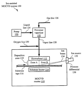
As a first embodiment of the invention, Figure 1 illustrates an ion-assisted
MOCVD
system 100 in accordance with the invention for producing lugh-current HTS-
coated
tapes by depositing HTS thick film with increased current capability. The ion-
assisted
MOCVD system 100 of the present invention includes a conventional MOCVD
reactor
110, which is a vacuum-sealed deposition chamber in which an MOCVD process
occurs,
such as a cold-wall reactor that may be maintained at a pressure of, for
example, 1.6 Torr.
The MOCVD reactor 110 houses a showerhead 112 located in close proximity to a
substrate heater 114. A substrate tape 116 is positioned and translates
(during operation)
between the showerhead 112 and the substrate heater 114 within a deposition
zone 118
formed along the length of the showerhead 112, i.e., the area in which the
substrate tape
116 is exposed to the precursor vapors. Furthermore, multiple regions within
the
deposition zone 118 are established, for example, a zone A and a zone B as
shown in
Figure 1.
7
CA 02527870 2005-11-30
WO 2005/007918 PCT/US2004/016597
The substrate tape 116 is a flexible length of substrate formed from a variety
of materials,
such as stainless steel or a nickel alloy such as Inconeh, upon which buffer
layers, such as
yttrium-stabilized zirconia (YSZ) andlor cerium oxide (Ce02) have been
previously
deposited. The substrate tape 116 is capable of withstanding temperatures up
to 950 °C
and has dimensions that may vary to meet the desired finished product and
system
limitations. For example, the substrate tape 116 may have a thickness of 25
microns, a
width of 1 cm, and a length of 100 meters.
The showerhead 112 is a device for uniformly distributing precursor vapors
onto the
substrate tape 116. The surface of the showerhead 112 that is oriented toward
the
substrate tape 116 includes multiple fine holes evenly distributed throughout
its area,
through which the precursor vapors exit toward the substrate tape 116. The
length of the
showerhead 112 and the specific composition of the vapor precursors feeding
the
showerhead 112 may be user defined depending on the application.
During the deposition process, the temperature of the substrate tape 116 is
controlled via
the substrate heater 114. The substrate heater 114 is a well-known single or
multiple
zone substrate heater that provides heating, typically in the range of 700 to
950 °C, to the
substrate tape 116 via a radiant heating element, such as a lamp.
Alternatively, the
substrate heater 114 is a resistance heater having a heating element, such as
I~anthal or
MoSi2.
CA 02527870 2005-11-30
WO 2005/007918 PCT/US2004/016597
The ion-assisted MOCVD system 100 further includes a system for the delivery
of
coating precursors. An exemplary precursor delivery system includes a pump 120
that is
fed by a liquid precursor source (not shown) that contains a solution
containing
organometallic precursors, such as tetramethyl heptanedionate (THD) compounds
of
yttrium (Y), barium (Ba), and copper (Cu), along with an appropriate mixture
of solvents,
such as tetrahydrofuran and isopropanol. The pump 120 is a high-pressure, low
flow rate
pump, such as a high-pressure liquid chromatography (HPLC) pump, capable of a
low
flow rate between 0.1 and 10 mL/min. The pump 120 feeds a precursor vaporizer
122 via
a liquid line 124 formed of tubing or piping.
The precursor vaporizer 122 is a well-known device in which a precursor
solution is flash
vaporized and mixed with an inert carrier gas, such as argon or nitrogen, for
delivery to
the showerhead 112. The inert carrier gas is fed into the precursor vaporizer
122 via a
gas line 126 formed of tubing or piping. The precursor vapors exit the
precursor
vaporizer 122 via a precursor vapor line 128 that connects to the inlet of the
showerhead
112. The vapor line 128 is a connecting tube or pipe through which the
precursor vapor
and its inert carrier gas pass on their way from the precursor vaporizer 122
to the
showerhead 112.
Just prior to the vapor line 128 entering the MOCVD reactor 110, an oxygen
line 130
opens into the vapor line 128. The oxygen line 130 is a tube or pipe through
which
9
CA 02527870 2005-11-30
WO 2005/007918 PCT/US2004/016597
oxygen passes for introduction to the precursor vapor and its inert carrier
gas flowing
within the vapor line 128.
The ion-assisted MOCVD system 100 includes an ion source 132 that emits an ion
beam
134 that is directed toward the substrate tape 116 within the MOCVD reactor
110. The
ion source 132 may be an inexpensive gridless ion bombardment source that is
capable of
generating a collimated or non-diffused ion beam at a power level typically in
the range
of 0.5 to 10 KW. An example of the gridless ion source 132 is commercially
available
from Veeco Instruments, [2330 E Prospect Fort Collins, CO X0525] operates at
voltages
up to 100-1000 eV, and has dimensions of 6 cm by 66 cm. The size and
orientation of
the ion source 132 is determined based on the length of the substrate tape 116
irradiated
and the design of the MOCVD reactor 110. The ion source 132 does not have to
be
located in close proximity to the deposition zone 118, as the ions of ion beam
134 can
travel long distances.
Alternatively, the ion source 132 may be a gridded ion source. However, a
gridded ion
source is likely to be less desirable than a gridless ion source because,
typically, gridded
ion sources are more costly than gridless ion sources and function with more
stringent
pressure requirements than gridless ion sources, i.e., 104 to 10--~ Torr as
compared with
10-2 to 10-3 Torr for gridless ion sources.
CA 02527870 2005-11-30
WO 2005/007918 PCT/US2004/016597
The pressure interface between the ion source 132 and the MOCVD reactor 110 is
accomplished via a pressure differential 136 mounted within the outer wall of
the
MOCVD reactor 110. The pressure differential 136 is a device that allows the
ion source
132 to be held at a typical vacuum pressure in the range of approximately 10-4
to 10-2
Torr, while at the same time allowing the MOCVD reactor 110 to be held at a
vacuum
pressure typically in the range of 1-50 Torr. This can be accomplished by
means of a
turbomolecular pump or a cryopump. The pressure differential 136 also includes
an
opening that allows the ion beam 134 to pass into the MOCVD reactor 110.
With reference to the ion-assisted MOCVD system 100 of Figure 1, the basic
MOCVD
process is well known in the art and can be summarized as follows. Within the
MOCVD
reactor 110 of the ion-assisted MOCVD system 100, HTS film, such as YBCO, is
deposited by vapor-phase precursors onto the heated substrate tape 116 via
chemical
reactions that occur at the surface of the substrate tape 116. More
specifically, the linear
translation of the substrate tape 116 through the deposition zone 118 begins
in a direction
progressing from zone A to zone B (the mechanisms for translating the
substrate tape 116
are not shown), the pump 120 is activated, the precursor vaporizer 122 is
activated, and
the substrate heater 114 is activated.
The vapor line 128 delivers the yttrium-barium-copper vapor precursor to the
showerhead
112, which uniformly directs this vapor precursor toward the substrate tape
116 within
the deposition zone 118. The result of the oxygen reacting with the yttrium-
barium-
11
CA 02527870 2005-11-30
WO 2005/007918 PCT/US2004/016597
copper vapor precursors and then this reacting combination coming into contact
with the
heated substrate tape 116 within the deposition zone 118 causes the yttrium-
barium-
copper vapor precursor to decompose and form a layer of YBCO atop the
substrate tape
116 as it translates through the deposition zone 118.
The substrate tape 116 experiences the initial accumulation of YBCO film
within zone A
of the deposition zone 118 where the film thickness builds from zero microns
up to 1.0 to
1.5 microns. The substrate tape 116 subsequently experiences further
accumulation of
YBCO film within zone B of the deposition zone 118, where the film thickness
continues
to build from approximately 1.5 microns up to 5 microns.
Concurrent with the normal deposition process occurring within the ion-
assisted
MOCVI~ system 100 as described above, the ion source 132 is activated and thus
emits
the ion beam 134. The stream of positive ions forming the ion beam 134 is
accelerated
toward the substrate tape 116 within the deposition zone 118. More
specifically, the ion
beam 134 emitting from the ion source 132 is focused upon the substrate tape
116 as it
translates through zone B of the deposition zone 118, where the YBCO film is
further
accumulating and approaching and/or exceeding a thickness of 1.5 microns.
Although
the process is shown as having two deposition zones A and B, there may be
multiple
deposition zones, with the requirement that those deposition zones where the
substrate
has a coating in excess of 1.5 microns thick, have an ion source focused on
the substrate
tape as it translates through that deposition zone. While it is not an
absolute requirement,
12
CA 02527870 2005-11-30
WO 2005/007918 PCT/US2004/016597
it may be preferable to have the ion source focused on the substrate even in
the first
deposition zone where the film is grown to a thickness of 1.5 microns. In this
way, it
could be assured that a template of a dense film is available for subsequent
growth.
As a result, the YBCO deposition process occurring within zone B of the
deposition zone
118 is influenced by the ion bombardment provided by the ion beam 134. Due to
this ion
bombardment, additional energy is added to the deposition process within zone
B of the
deposition zone 118, which has the effect of minimizing film defects, such as
lugh
porosity, voids, and surface roughness, thereby maintaining a high-quality
growth
template as the YBCO film accumulates by vapor deposition upon the substrate
tape 116.
As a result, the ion-assisted MOCVD system 100 of the present invention is
capable of
producing a YBCO film with a thickness in excess of 1.5 microns that has
increased
material density and smoothness that results in increased current capacity.
There is no particular orientation requirement for the ion source 132 in
relation to zone B.
Rather, the orientation is governed by the design of the MOCVD reactor 110
because
there is an optimum distance between the substrate tape 116 and the showerhead
112. In
particular, the orientation of the incident ion beam 134 is governed by the
dimension of
the showerhead 112 and the substrate heater 114.
The ion beam 134 from the ion source 132 is not focused upon the substrate
tape 116
within zone A of the deposition zone 118 where the YBCO film is forming with a
13
CA 02527870 2005-11-30
WO 2005/007918 PCT/US2004/016597
thickness that is less than, for example, 1.0 to 1.5 microns. This is because,
as stated
above, the quality of the YBCO film morphology within the first 1.0 to 1.5
microns of
growth is very high and the current capacity is not inhibited.
Although not required to obtain the benefits of the present invention, the ion
beam may
be allowed to impinge upon the substrate in zone A as well. Ion bombardment
may be
used within zone A of the deposition zone 118 where the thickness of the YBCO
film is
less than 1.0 to 1.5 microns to assure that the film is dense, thereby
providing a good
template for subsequent layers.
Figure 2 illustrates a second embodiment of the invention, an ion-assisted PLD
system
200 for producing high-current HTS-coated tapes by depositing HTS thick film
with
increased current capability. The ion-assisted PLD system 200 of the present
invention
includes a conventional deposition chamber 210, which is a vacuum chamber
designed
specifically for pulsed laser deposition applications. An example of such a
vacuum
chamber is a 12- or 1 ~-inch vacuum chamber commercially available by Neocera,
[ 10000
Virginia Manor Road Beltsville, MD 20705] although those skilled in the art
will
appreciate that a number of alternative vendors manufacture vacuum chambers in
a
variety of shapes and sizes. The deposition chamber 210 is maintained at a
pressure of,
for example, 200 mTorr. In this example, the deposition chamber 210 houses a
first
target 212 and a second target 214 that are located in close proximity to a
substrate heater
216. The substrate tape 116 as described in Figure 1 is positioned and
translates (during
14
CA 02527870 2005-11-30
WO 2005/007918 PCT/US2004/016597
operation) between the targets 212 and 214 and the substrate heater 216. The
targets 212
and 214 are composed of HTS material, such as YBCO, and are available
commercially
from suppliers such as Praxair Surface Technologies, Specialty Ceramics [16130
Wood-
Red Rd., #7, Woodinville, WA 98072] and Superconductive Components, Inc. [1145
Chesapeake Ave., Columbus, OH 43212].
During the deposition process, the temperature of the substrate tape 116 is
controlled via
the substrate heater 216. Like the substrate heater 114 of Figure 1, the
substrate heater
216 is a well-known single or multiple zone substrate heater that provides
heating,
typically in the range of 750 and 830 °C, to the substrate tape 116 via
a radiant heating
element such as a lamp.
Finally, the ion-assisted PLD system 200 includes an ion source 218 that emits
an ion
beam 220 that is directed toward the substrate tape 116 within the deposition
chamber
210. The ion source 218 is an inexpensive gridless ion bombardment source that
is
capable of generating a collimated or non-diffused ion beam at a power level
typically in
the range of 0.5 to 10 KW. An example of a gridless ion source 218 is
commercially
available from Veeco Instruments, [2330 E Prospect Fort Collins, CO 80525]
operates at
voltages up to 100-1000 eV, and has dimensions of 3 to 6 cm in diameter. The
size of the
ion source 218, especially the length of the ion source 218, is the similar to
the length of
the film deposition zone.
CA 02527870 2005-11-30
WO 2005/007918 PCT/US2004/016597
There is no particular orientation of the ion source 218 relative to the film
deposition
zone. Rather, the orientation is governed by the design of the deposition
chamber 210
because there is an optimum distance between the substrate tape 116 and the
targets 212
and 214. In particular, the orientation of the incident ion beam 218 is
governed by the
dimension of the targets 212 and 214 and the substrate heater 216. The ion
source 218
does not have to be located in close proximity to the substrate tape 116, as
the ions of ion
beam 220 can travel long distances. Alternatively, the ion source 218 is a
gridded ion
source.
With reference to the ion-assisted PLD system Z00 of Figure 2, the basic PLD
process is
well known in the art and need only be surmnarized as follows. Within the
deposition
chamber 210 of the ion-assisted PLD system 200, HTS film, such as YBCO, is
deposited
by the evaporation of HTS material and the subsequent exposure of the heated
substrate
tape 116 to this evaporant. More specifically, the linear translation of the
substrate tape
116 through the deposition chamber 210 begins in a direction that first passes
by the
target 212 and then by the target 214 that are arranged along the substrate
tape 116 line of
travel (the mechanisms for translating the substrate tape 116 are not shown).
The
substrate heater 216 is activated.
A first laser source (not shown) is activated and generates a laser beam 222
that impinges
upon the surface of the target 212, causing the formation of a plume 224,
which emanates
from that portion of the target 212 radiated by the laser beam 222 toward the
substrate
16
CA 02527870 2005-11-30
WO 2005/007918 PCT/US2004/016597
tape 116 in a highly forward-directed fashion. In like manner, a second laser
source (not
shown) is activated and generates a laser beam 226 that impinges upon the
surface of the
target 214, causing the formation of a plume 228, which emanates from that
portion of
the target 214 radiated by the laser beam 226 towaxd the substrate tape 116 in
a highly
forward-directed fashion.
The plumes 224 and 228 are plasma clouds resulting from the material of
targets 212 and
214, respectively, melting and subsequently evaporating explosively when
impinged
upon by the laser beams 222 and 226, respectively.
The YBCO particles contained in the plume 224 are thus deposited onto the
surface of the
substrate tape 116 as the tape translates through the deposition chamber 210
at a
predetermined speed.
The substrate tape 116 experiences the initial accumulation of YBCO film via
exposure
to the YBCO particles contained in the plume 224 as the substrate tape 116
translates
through the deposition chamber 210 at a predetermined speed. Due to exposure
to the
particles of the plume 224, the film thickness upon the surface of the
substrate tape 116
builds from zero microns up to 1.0 to 1.5 microns. The substrate tape 116
subsequently
experiences further accumulation of YBCO film via exposure to the YBCO
particles
contained in the plume 228 as the substrate tape 116 translates through the
deposition
chamber 210 at a predetermined speed. Due to exposure to the particles of the
plume
17
CA 02527870 2005-11-30
WO 2005/007918 PCT/US2004/016597
228, the film thickness upon the surface of the substrate tape 116 builds from
approximately 1.5 microns up to 5 microns.
Concurrent with the normal deposition process occurring within the ion-
assisted PLD
system 200 as described above, the ion source 218 is activated and thus emits
the ion
beam 220. The stream of positive ions forming the ion beam 220 is accelerated
toward
the substrate tape 116 and is focused upon the substrate tape 116 as it
translates through
the particles of the plume 228 where the YBCO film is further accumulating and
approaching and/or exceeding a thickness of 1.5 microns. As a result, the YBCO
deposition process occurnng via exposure to the particles of the plume 228 is
influenced
by the ion bombardment provided by the ion beam 220. Although the process is
shown
as having two plumes, there may be multiple plumes, with the requirement that
those
deposition zones where the substrate has a coating in excess of 1.5 microns
thick, have an
ion source focused on the substrate tape as it translates through the plume
defining that
deposition zone.
Due to this ion bombardment, additional energy is added to the deposition
process
occurnng due to exposure to the particles of the plume 228, wluch has the
effect of
minimizing film defects, such as high porosity, voids, and surface roughness,
thereby
maintaining a high-quality growth template as the YBCO film accumulates by
vapor
deposition upon the substrate tape 116. As a result, the ion-assisted PLD
system 200 of
the present invention is capable of producing a YBCO film with a thickness in
excess of
18
CA 02527870 2005-11-30
WO 2005/007918 PCT/US2004/016597
1.5 microns that has increased material density and smoothness that results in
increased
current capacity.
The ion beam 220 from the ion source 218 need not be focused upon the
substrate tape
116 as it is exposed to the plume 224 where the YBCO film is forming with a
thickness
that is less than, for example, 1.0 to 1.5 microns. This is because, as stated
above, the
quality of the YBCO film morphology within the first 1.0 to 1.5 microns of
growth is still
very high and, thus, the current capacity is not inhibited.
Alternatively, however, ion bombardment may be used in the area where the
substrate
tape 116 is exposed to the plume 224 where the thickness of the YBCO film is
less than
1.0 to 1.5 microns. In particular, using ion bombardment in the area where the
substrate
tape 116 is exposed to the plume 224 can assure that the film is dense,
thereby providing
a good template for subsequent layers.
19