Note: Descriptions are shown in the official language in which they were submitted.
CA 02528061 2005-12-02
WO 2004/110107 PCT/US2004/017407
ENERGY SAVINGS DEVICE AND METHOD FOR A RESISTIVE
AND/OR AN INDUCTIVE LOAD AND/OR A CAPACITIVE LOAD
RELATED APPLICATIONS
~ This application is a continuation-in-part of U.S. patent application serial
number 10/205,031, filed July 26, 2002, whereby this application also claims
priority to provisional patent application 60/336,222, filed November I4,
2001.
BACKGROUND OF THE INVENTION
A. FIELD OF THE INVENTION
tooozl The invention relates to an energy savings device or method that can be
applied to a resistive, an inductive, or a capacitive load regardless of the
respective impedance or inductance or capacitance of the load. More
particularly, the invention relates to a reactive load dimming device that is
mounted in series with a resistive, an inductive or a capacitive load and that
has
access for power and operation to one side of an electrical line supplied to
the
load. A fluorescent light fixture or a motor for a fan or other device, for
example, can be controlled by way of an energy savings device or method
according to the invention.
CA 02528061 2005-12-02
WO 2004/110107 PCT/US2004/017407
B. DESCRIPTION OF THE RELATED ART
~ooos~ The ability to control illumination levels is strongly desired,
especially due
to the rising energy costs. Such ability to control illumination levels is
very
important for establishments that require a great deal of lighting, such as
restaurants and off ces.
a~ Lighting levels that are higher than necessary not only result in a higher
energy costs associated with the lighting, but also can increase air
conditioning
costs due to the excess heat provided by the lighting fixtures. Fluorescent
tight
fixtures output less heat than incandescent light fixtures for equivalent
illumination, and thus they are becoming more popular with offices or other
commercial establishments.
There currently exist various types of dimmer devices that can be used in
order to control the amount of light output by fluorescent lights. One type
utilizes a complex electronic ballast which first converts the applied AC Line
voltage to DC, then switches the applied tube voltage at high frequency. The
resulting power-to-light output efficiency is hampered by this additional
manipulation. This type requires an expensive fixture replacement and rewiring
to the wall switch. Simplistic phase control devices will not provide
satisfactory
results when controlling a magnetic ballast fluorescent fxture.
-2-
CA 02528061 2005-12-02
WO 2004/110107 PCT/US2004/017407
s~ Figure IA showws the connections of a conventional fluorescent dimmer
device or controller 100, which is provided between a. line and a load. The
load
is shown as a light fixture 110, which may be a fluorescent tube and
associated
ballast, for example. As shown in Figure lA, the conventional controller 100
needs access to both sides (tine 102 and neutral 104) of an AC power input, in
addition to the load. Since connectivity to the neutral line 104 is not always
available at a light switch box, conventional fluorescent controllers may
require
expensive re-wiring to be installed.
1 The problem with using such a conventional dimmer circuit for a
fluorescent lighting fixture is that the conventional dimmer circuit cannot
modulate reactive loads. Reactive loads react with the controller, thereby
producing oscillations that then cause surges of voltage and current, which
are
both unpredictable and uncontrollable. With such control being applied to a
fluorescent light fixture, the typical result is a non-harmonic type of
flickering,
which frequently takes the light from zero output to maximum output and to
values in between. Such flickering is visually (and also audibly)
discomforting,
and may even be unhealthful to people who are near the flickering fluorescent
light (for example, it may cause headaches due to having to view the
undesirable
light flickering).
-3-
CA 02528061 2005-12-02
WO 2004/110107 PCT/US2004/017407
tooos~ As explained earlier, a controller such as the one shown in Figure lA
can
be used to control a fluorescent light without causing significant flickering,
but
such a controller requires fairly substantial installation costs, since they
cannot be
installed at a light switch box (where a neutral line is not typically
provided), but
rather have to be installed very close to the ballast (e.g., in the ceiling of
a room,
where a neutral line is provided).
~ U.S. Patent No. 5,043,635 to Talbott et al. describes a two-line power
control device for dirnrning fluorescent lights, which does not require to be
-coupled-to a. neutral line. Accordingly, the Talbott et al. device can in
theory be
installed at a light switch box. However, due to the analog structure and the
various components described in the Talbott et al. device, such a device is
very
difficult to manufacture, and also such a device is very difficult to
manufacture in
a small size. Thus, 'it is not feasible to install such a device in a light
switch box,
given the bulkiness as well as the transformer configuration of the Talbott et
al.
device.
SUMMARY OF THE INVENTION
_4_
CA 02528061 2005-12-02
WO 2004/110107 PCT/US2004/017407
~ The present invention is directed to an apparatus and a method for
controlling an amount of power supplied to a resistive, inductive or
capacitive
load by modulating a period of time that current flows through the load.
goo"~ According to one aspect of the invention, there is provided an energy
savings device for an inductive, resistive or capacitive load that is powered
by an
input AC voltage waveform. The device includes a setting unit for setting a
desired power operating level for the load. The device also includes a
microprocessor configured to receive a signal from the setting unit indicative
of
the desired power operating level for the load, to determine a phase delay to
be
provided to an output AC voltage waveform that is to be provided to the load,
and to output a control signal as a result thereof. The device further
includes an
active element provided between a line that provides the input AC voltage
waveform and the load, the active element receiving the control signal and
turning off and on at predetermined times in accordance with the control
signal,
so as to create the output AC voltage waveform from the input AC voltage
waveform.
~oo,z~ According to another aspect of the invention, there is provided an
energy
savings method for an inductive, resistive or capacitive load that is powered
by
an input AC voltage waveform. The method includes setting a desired power
-S-
CA 02528061 2005-12-02
WO 2004/110107 PCT/US2004/017407
operating level for the load. The method further includes receiving a signal
indicative of the desired power operating level for the load, and determining
a
phase delay to be provided to an output AC voltage waveform that is to be
provided to the load, and to output a control signal as a result thereof. The
method also includes receiving the control signal, and, in response thereto,
turning an active element off and on at predetermined times in accordance with
the control signal, so as to create the output AC voltage waveform from the
input
AC voltage waveform. The active element is disposed between a line carrying
the_input AC voltage waveform and the load.
~ According to yet another aspect of the invention, there is provided a
computer program product for providing energy savings for an inductive,
resistive or capacitive load that is powered by an input AC voltage waveform.
The computer program product includes first computer code configured to set a
desired power operating level for the load. The computer program product also
includes second computer code configured to receive a setting signal output
from
the first computer code that is indicative of the desired power operating
level for
the load, the second computer code further configured to determine a phase
delay
to be provvided to an output AC vvoltage waveform that is to be provided to
the
load, and to output a control signal as a result thereof. The computer program
-6-
CA 02528061 2005-12-02
WO 2004/110107 PCT/US2004/017407
product further includes third computer code configured to provide a control
signal to an active element provided between a line that provides the input AC
voltage waveform and the load, the active element receiving the control signal
and turning off and on at predetermined times in accordance with the control
signal, so as to create the output AC voltage waveform from the input AC
voltage waveform. The control signal is provided based on the phase delay
determined by the second computer code and the setting signal output by the
first
computer code.
According to yet another aspect of the invention, there is provided an
energy savings device for an inductive, resistive or capacitive load that is
powered by an input AC voltage waveform. The energy savings device includes
setting means for allowing a user to set a desired power operating Level for
the
load. The energy savings device also includes processing means for receiving a
signal from the setting unit indicative of the desired power operating level
for the
load, and for determining a phase delay to be provided to an output AC voltage
waveform that is to be provided to the load, and to output a control signal as
a
result thereof. The energy savings device further includes signal conversion
means, provided between a line that provides the input AC voltage waveform and
the load, for receiving the control signal and turning off and on at
predetermined
CA 02528061 2005-12-02
WO 2004/110107 PCT/US2004/017407
times in accordance with the control signal, so as to create the output AC
voltage
waveform from the input AC voltage waveform.
BRIEF DESCRIPTION OF THE DRAWINGS
(0015 The foregoing advantages and features of the invention will become
apparent upon reference to the following detailed description and the
accompanying drawings, of which:
Figure lA shows a hookup of a conventional energy savings~device that is
provided between an input voltage line and a load;
Figure 1 B shows a hookup of an energy savings device according to an
embodiment of the invention that is provided between an input voltage line and
a
load;
~oo,s~ Figure 2 shows an alternative hool.-up of an energy savings device
according to an embodiment of the invention that provides neutral side
control;
[0019] Figure 3 is a block diagram of an energy savings device according to a
first
embodiment of the invention;
toozo~ Figure 4 is a schematic circuit diagram of an energy savings device
according to the first embodiment of the invention;
_g_
CA 02528061 2005-12-02
WO 2004/110107 PCT/US2004/017407
[0021] Figure 5 shows phase control waveforms according to the first
embodiment
of the invention;
~oozz~ Figure 6 is a software flow diagram of microprocessor firmware that
operates according to the first embodiment of the invention;
~oozs~ Figure 7 is a block diagram of an energy savings device according to a
second embodiment of the invention;
~ooza~ Figure 8 is a schematic circuit .diagram of an energy savings device
according to the second embodiment of the invention;
[.Q025] Figure 9. is a schematic circuit diagram of a master unit according to
a
seventh embodiment of the invention; and
~oozs~ Figure 10 is a schematic circuit diagram of a follower unit according
to the
seventh embodiment of the invention.
DETAILED DESCRIPTION OF THE INVENTION
~oozl~ Preferred embodiments of the invention will be described in detail
below,
with reference to the accompanying drawings.
~ooza~ The invention is directed to an apparatus and method for controlling
power
to a resistive, an inductive or a capacitive load, such as a fluorescent light
fixture, a halogen light fixture, or a motor for a fan. In a preferred
-9-
CA 02528061 2005-12-02
WO 2004/110107 PCT/US2004/017407
configuration, the energy controlling apparatus is configured to be installed
in a
light switch box typically located on an interior wall of a building, behind a
wall
switch plate. Since most light switches are mounted within a switch box that
is
easily accessible. through-the wall (e.g., behind a switch plate), the line to
the
switch is dropped from the fixture to the switch, and the other side of the
line
(e.g., neutral) is not conveniently present. The invention provides a true
switch
replacement and operates in series with an inductive or resistive load, in a
two-
wire configuration, plus safety ground wire. Figure 1 B shows a hookup of an
energy savings device 150 according to an embodiment of the invention that is
provided between the input AC line voltage 102 and a reactive load 110,
whereby
hookup to the neutral line 104 is not required by the energy savings device
150 in
order to provide an energy control function for the load 110.
Additionally, referring now to Figure 2, some installations will wire the
line 102 directly to the light fixture 110, leaving the load return 103 for
fixture
control. In this case, there is no line 102 connection in the switch box,
again
disallowing integration of a conventional fluorescent dimmer device. The UCD
controller 150 is fully compatible with neutral 104 side control, in the
manner as
shown in Figure 2. In summary, the UCD controller according to the different
embodiments of the invvention is installed in series with the load, on either
side of
-10-
CA 02528061 2005-12-02
WO 2004/110107 PCT/US2004/017407
the load, without regard to wiring polarity, identically to a dry contact
switch
installation.
With regards to fluorescent light fixtures, the energy savings device
according to the invention regulates a voltage output to gaseous discharge
lamps
of the fluorescent light fixture from the secondary coils of a ballast element
of the
fluorescent light fixture.
~oos,~ A universal control device (or UCD) according to a first embodiment of
the invention will be described below in detail. A block diagram of the UCD
according. to the first embodiment is shown in Figure 3, and a schematic
circuit
diagram of the UCD according to the first embodiment is shown in Figure 4.
[0032] The UCD according to the first embodiment includes a "push" On/Off
switch and potentiometer unit 310 that is coupled to a line input (AC input
voltage) 305, a solid state switch unit 320, a driver 330 for driving the
solid state
switch unit 320, a power supply 340, a microprocessor 350, and a line
synchronization detector 360. The solid state switch unit 320 is provided
between the line input 305 and the load 365. The switch and potentiometer unit
310 includes a "push" On/Off switch SW1 and a potentiometer POT. The line
synchronization detector 360 provides an interrupt signal to the
microprocessor
-11-
CA 02528061 2005-12-02
WO 2004/110107 PCT/US2004/017407
350, which corresponds to "rising" zero crossing of a load current waveform,
to
be explained in more detail below.
[0033] The UCD is a two wire dimlTier unit, and can be utilized to control
standard magnetic fluorescent fixtures. The UCD may also be used to control
other resistive, inductive or capacitive (e.g. , standard electronic
fluorescent
fixtures) loads. The UCD filnctions similar to incandescent dimmers, but it
also
implements line synchronization functions and timing functions (not done by
incandescent dimmers) to allow it to control fluorescent fixtures and/or other
types of reactive or capacitive loads. In a preferred configuration, the UCD
is
wired in series with the fluorescent load without observance of wiring
polarity, in
either the hot or return side of the load, in a manner that is identical to a
standard
single pole wall switch. In fact, the UCD is configured so as to replace any
existing wall switch to provide a dimming functionality.
[0034) In a preferred implementation of the first embodiment, the UCD
implements an 8-bit digital microprocessor 350 (of course, other types of
microprocessors, such as 16-bit, 32-bit, etc., may be utilized instead of an 8-
bit
microprocessor, while remaining within the scope of the invention) with
embedded firmware control algorithms for minimum parts count, and highly
stable operation. The UCD according to the first embodiment is compatible with
-12-
CA 02528061 2005-12-02
WO 2004/110107 PCT/US2004/017407
any configuration of magnetic ballast or electronic ballast fluorescent and/or
incandescent loads. In a preferred construction, unit size, costs,
producibility,
performance and stability are optimized through the use of advanced digital
and
mass production techniques. Other embodiments to be described later include
occupancy sensing, ambient light correction, and AC line modem for
communication with a remote Energy Management System. All of the
embodiments to be described herein are "in series", two wire devices (see
Figure
1 B or Figure 2).
~oo3s~ Table 1 provides line specifications of the UCD according to a
preferred
implementation of the first embodiment of the invention. One of ordinary skill
in
the art will recognize that other line specification ranges may be handled by
the
UCD according to the first embodiment, while remaining within the scope of the
invention.
~ooasl Table 1
Specifications
oltage 110/277 Vac
requency 50/60 Hz
oad Current 6.3 Amps Maximum
oad/Watts 750 Watts Maximum
ower Factor 0.87-0.90 (full power)
HD < 35% (full power)
-13-
CA 02528061 2005-12-02
WO 2004/110107 PCT/US2004/017407
IIEMI/RFI FCG Part 18 II
The UCD according to the first embodiment provides AC line
synchronization and timing firmware algorithms used to provide stable dimming
control of an inductive and/or resistive and/or capacitive load without regard
to
applied line voltage, frequency, and without requiring a specific connection
to the
AC Line Return or Safety Ground. The UCD according to the first embodiment
implements phase control of the load, and also strategically controls the
switching
element turn-on timing for stable (non-flickering) control of inductive or
resistive
locos: The iJCD-accor'd~ing tomthe~ first-embodiment synchronizes on the load
current zero crossing, which causes a turning off of the series switching
elements
making up the solid state switch unit 320.
~oo3s~ Highly inductive or resistive loads, such as magnetic fluorescent
ballasts,
cause a significant phase shift (delay) of the load current waveform relative
to the
applied voltage waveform, greatly complicating stable synchronization. This
phase shift varies depending on the specific installation,(number of fixtures
and
specific ballast specifications) as well as the selected dimming level. As the
dimming level is varied, or fluorescent tube temperature changes,, the current
zero crossing synchronization signal to the microprocessor will move
significantly in real time, causing a shift in phase timing for the next
cycle.
-14-
CA 02528061 2005-12-02
WO 2004/110107 PCT/US2004/017407
Unless a suitable phase timing algorithm is implemented, the light fixture
will
flicker in an oscillatory way, resulting in unstable (highly unsatisfactory)
dimming. The inventors of this application realized that standard incandescent
dimmers will not reliably function with fluorescent or other types of reactive
loads due to their simplistic line synchronization methods. The timing
correction algorithms utilized in the present invention are an important
aspect of
the UCD design according to the first embodiment (as well as to the other
embodiments), and are described in detail below. Also, the UCD according to
the present invention also performs well as a dimmer control with little or no
flickering, for an electronic fluorescent ballast, which is a capacitive load.
Figure ~ shows the applied line voltage waveform, the dimmed fluorescent
load current waveform, and the microprocessor synchronization waveform as
implemented by the UCD according to the first embodiment. Also shown in
Figure S are seven (7) time points in a single cycle of the applied line
voltage
waveform (60 Hz or 16.67 msec time period for one cycle), each of which is
discussed in detail below. The highly inductive nature of a fluorescent
magnetic
ballast causes the load current to lag the applied line voltage, as seen in
the
comparison of the AC line voltage waveform 510 with the load current waveform
520. The amount of lag depends on the circuit inductance, specific ballast
design .
-15-
CA 02528061 2005-12-02
WO 2004/110107 PCT/US2004/017407
factors, tube striking voltage which is affected by tube temperature, and the
amount of dimming phase delay being applied by the UCD according to the first
embodiment. A point by point discussion of the seven labeled time points in
Figure 5 follows, with reference to the circuit elements shown in Figure 4.
Time point 1 corresponds to the rising zero crossing of the applied line
voltage waveform 510.
[0041] Time point 2 corresponds to the turn off point of Silicon Controlled
Rectifier (SCR) Q2 from the previous dim cycle. An SCR turns off when the
appliecLcurr_ent_th.rough_it reaches zero. Once the SCR turns off, the voltage
across the SCR rises sharply.
[0042] At time point 3, the turning off of SCR Q2 causes the synchronization
signal on pin 5 of the microprocessor U2 to go low, which interrupts the
microprocessor U2. In the preferred implementation of the first embodiment,
microprocessor firmware is initialized to only respond to the falling edge of
the
interrupt, and is used to derive all phase control timing for an entire line
cycle.
As the UCD dimmer potentiometer R7 is rotated clockwise, the period of phase
delay time between time point 3 and time point 4 of Figure 5 is increased,
causing the fluorescent light fixture being controlled by the UCD to dim.
Conversely, counterclockwise rotation of the UCD dimmer potentiometer .R7
-16-
CA 02528061 2005-12-02
WO 2004/110107 PCT/US2004/017407
decreases this phase delay time, thereby causing the fluorescent light fixture
light
output amount to intensify.
[0043] The inventors have found through experimentation that a typical
fluorescent tube with magnetic ballast goes off (no light output by it) at
approximately 120 degrees (about 5. S mseconds) of phase delay. This is due to
insufficient tube ionization caused by' insufficient tube heater output.
Without
adequate tube ionization, the tube strike voltage exceeds that available from
the
AC line. The inventors have also found that they were not able to visibly
discern
a change in light output until the phase delay reached about 15 degrees (about
0.7
mseconds) of phase delay. The half intensity point was about g0 degrees of
phase delay (about 4.17 mseconds).
Microprocessor control of the phase delay controls the dim level of the
fluorescent fixture (the load). In response to the falling edge of the
synchronization interrupt, the microprocessor U2 resets a free-running
internal
hardware timer (not shown in the figures) to zero, then waits for the timer to
reach the phase delay value corresponding to the current position of the UCD
dimmer potentiometer R7. In a preferred implementation, the UCD dimmer
potentiometer R7 is coupled to a rotatable dial that is disposed on a wall of
a
building, whereby, when a user rotates the dial, the resistance of
potentiometer
-17-
CA 02528061 2005-12-02
WO 2004/110107 PCT/US2004/017407
R7 changes accordingly. The change in the resistance of potentiometer R7 is
discerned by the microprocessor U2, which then computes a different phase
delay value for a next AC voltage waveform cycle based on the new dimmer
setting.
[0045] After the calculated phase delay time corresponding to time point 4 is
reached, the microprocessor U2 triggers the SCR Q1 on by bringing pin 2 of the
microprocessor U2 low for a short period of time. In the preferred
construction,
an opto-isolated triac U1 is used to trigger the SCR on while isolating the
micr_opr_ocessor U2 from possible damaging transients. Once the SCR Q1 is
triggered on and current begins to flow, SCR Q1 will latch itself on until
current
reaches zero during the next half cycle. Current flow through the load
continues
whenever the SCR Ql or the SCR Q2 is triggered on. When the SCR triggers
on, the synchronization signal 530 goes high again. The rising edge of the
synchronization signal 530 is ignored by the microprocessor U2, which only
reacts to a falling edge of the synchronization signal 530 (due to
microprocessor
firmware that allows interrupts only on the falling edge of a signal provided
to its
interrupt port).
Time point 5 corresponds to the next zero crossing of the load current
waveform 520. At this point, the SCR Ql turns off. Unlike the occurrence at
-18-
CA 02528061 2005-12-02
WO 2004/110107 PCT/US2004/017407
time point 2, no synchronization signal occurs at time point 5. This is
because
the microprocessor SV supply voltage (input line voltage) 340 is negative (it
is a
floating supply), and the open fluorescent circuit (that is, the load) is
roughly
ground. The synchronization signal 530 actually rises slightly (few tenths of
a
volt) after time point 5, because the "grounded" fluorescent circuit is
actually
higher in voltage than the microprocessor negative SV power supply 340.
Microprocessor firmware is provided such that no microprocessor interrupt is
generated from this slight perturbation of the synchronization signal 530 (and
also
since it does not correspond to a voltage drop but rather a voltage rise).
Phase control for the latter half cycle of the AC line voltage waveform 510
is derived from the previous earlier half cycle interrupt. The microprocessor
U2
measures the applied line frequency and computes the number of internal free-
running hardware timer counts that it has to wait for before triggering the
SCR
on for this latter half-cycle. The timer counts for a time period
corresponding
between the time between time point 5 and time point 6.
~ooas~ At time point 6, the SCR Q2 is triggered on. At time point 6, the
voltage
of the synchronization signal 530 drops slightly (a few tenths of a volt). No
microprocessor interrupt is generated here either, due to the microprocessor
firmware being configured to not cause an interrupt for such a small voltage
CA 02528061 2005-12-02
WO 2004/110107 PCT/US2004/017407
drop. Again, the SCR Q2 remains on during the negative half cycle, until the
circuit current reaches zero.
At time point 7, the rising load current waveform 520 again reaches zero.
Again the synchronization signal 530 goes to zero, which causes a .
microprocessor interrupt (since it is a falling edge of the synchronization
signal
530). This also causes a resynchronization of an internal free-running timer
of
the microprocessor U2, and results in another phase delay cycle similar to the
one that was described above with respect to the time point 2 and time point
3.
- The-UGD-hardware design according to a preferred configuration of the
first embodiment includes the components illustrated in the Figure 4 schematic
diagram. A brief description of each hardware component, and its applied
function, is provided below.
[0051] The microprocessor U2 (which corresponds to microprocessor 350 of
Figure 3) provides the control functions and algorithms for the UCD according
to
the first embodiment based on an internally stored firmware program. By way of
example and not by way of limitation, in a preferred implementation, a
MICROCHIP'''°2 1X672 eight bit microprocessor incorporates 2
kilobytes
programmable read only memory (PROM) for program storage, 128 bytes
random access memory (RAM), an eight bit timer, 4 channel.8 bit Analog to
-20-
CA 02528061 2005-12-02
WO 2004/110107 PCT/US2004/017407
Digital (A/D) converter, 4 MHz oscillator, and reset circuit in a very space
efficient 8 pin package. More details on this microprocessor can be found at
the
Internet web site www.microchip.com. Of course, one of ordinary skill in the
art will understand that other types and sizes of microprocessors may be
utilized
for the microprocessor to used in the first embodiment, while remaining within
the scope of the invention.
(0052] Since the functionality of the microprocessor U2 exists internally, in
a
preferred implementation, six I/O pins may be allocated to either digital
inputs
and outputs or analog inputs. Two pins are reserved for +5 volt power and
ground. By way of example and not by way of limitation, an Analog .to Digital
input impedance is approximately lOK ohms.
[0053) By way of example and not by way of limitation, the "push" on/off
potentiometer switch SW 1 is rated for the 6.3 ampere maximum dimming
capacity. When turned off, the dimmer/load is entirely open circuited,
resulting
in no current flow to the load. Rotating potentiometer R7 and switch SW 1 are
preferably integrated into a single unit. Pushing the adjustment shaft of
potentiometer R7 will cycle switch SW 1 on and off. Potentiometer R7 is wired
as an adjustable voltage divider, whereby rotating the shaft of potentiometer
R7
adjusts the voltage at pin 7 of microprocessor U2. The microprocessor U2 reads
-21-
CA 02528061 2005-12-02
WO 2004/110107 PCT/US2004/017407
the voltage at its pin 7 once every AC line cycle, and uses this voltage to
derive
the amount of phase delay (dim level) for the load. Resistor R8 is wired
between
the potentiometer wiper and ground, and is used to provide a more linear
relationship between the potentiometer position and resulting dim level. By
way
of example and not by way of limitation, resistor R8 has a resistance of 4.7
kohms.
(0054] In the preferred implementation of the UCD according to the first
embodiment, two SCRs Ql, Q2 are connected back to back to provide an active
-s-wi~tchi-ng ele -rn. ent .for-the-UC.D, and cor_re.spond to the solid state
switch 320 of
Figure 3. The inventors found that TRIAC devices do not trigger as accurately
as back-to-back SCRs when switching a highly inductive resistive load.
Consistent and accurate switching element rilrn-OFF at the current zero
crossing
is very important to line synchronization. The use of a TRIAC as the active
element may result in occasional flickering, which may be due to an unstable
holding current level.' As a result, the inventors found that an active
element that
includes back-to=back SCRs functions much better than one having a TRIAC in
the energy savings device according to the invention, whereby using two SCRs
provides an increase in switching current capability and better heat
distribution to
a heat sink.
-22-
CA 02528061 2005-12-02
WO 2004/110107 PCT/US2004/017407
[0055] By way of example and not by way of limitation, the SCRs utilized in a
preferred implementation of the first embodiment are 600V, 15 ampere devices.
The SCRs Q1, Q2 are designed to run very cool at maximum specified loads.
The choice of which type of SCRs to use in the first embodiment may also be
made based on a low holding current parameter for the SCRs. When a signal of
either polarity triggers the opto-isolated triac U1, positive pulses from pin
4 and
from pin 6 of the opto-isolated triac U1 are transmitted to gates (G) of the
SCRs
Q1, Q2, respectively. Opto-isolated triac U1 of.Figure 4 corresponds to solid
state_driver unit 330 shown in Figure 3.
~ooss~ SCRs conduct current in one direction (from anode to cathode), with
back-
l~to-back SCRs having the capability to conduct in both directions. SCRs are
latching devices; meaning that once they are trigger on, they will continue
conducting until the anode-to-cathode current through them reaches zero (or
reverses direction). An SCR is triggered on by pulling current out of its Gate
pin, or bringing the Gate voltage a few volts lower than its anode pin. The
holding current specification for an SCR specifies the minimum SCR current
necessary for the SCR to latch on, and to remain latched on. A holding current
on the order to 20 milliamperes is needed for proper operation of a typical
SCR.
Once the SCR current drops below the specified holding current, it will turn
off
-23-
CA 02528061 2005-12-02
WO 2004/110107 PCT/US2004/017407
until retriggered again. Only the SCR with its anode voltage positive relative
to
its cathode voltage is capable of being triggered on. This means that SCR Q1
controls the load during the positive half of the AC voltage waveform cycle,
and
SCR Q2 controls the load during the negative half of the AC voltage waveform
cycle: .
~oosn As shown best in Figure 4, the opto-isolated triac U1 is used to trigger
the
SCRs Q1, Q2. The microprocessor U2 triggers opto-isolated triac's U1 internal
triac, and subsequently one or the other SCR Q1, Q2, by illuminating the opto-
isolated_triac'_s_U_l..internal light emitting diode (LED). LED illumination
occurs
when the microprocessor U2 pulls its output pin 2 low, resulting in LED
forward
current. The opto-isolated triac U1 is capable of conducting current in either
direction, depending on the relative voltages of pins 4 and pin 6 of the opto-
isolated triac U1. For example, if pin 6 is higher than pin 4 of the opto-
isolated
triac U1, current will flow from pin 6 to pin 4. Connecting the opto-isolated
triac U 1 between the gates of the two SCRs Q 1, Q2 provides a convenient
method of triggering back-to-back SCRs.
~ooss~ Current flows into pin 6 of the opto-isolated triac U 1 and out pin 4
in
response to the positive half of the AC sine wave voltage waveform 510 (see
Figure 5) and vice versa in response to the negative half of the AC sine wave
24-
CA 02528061 2005-12-02
WO 2004/110107 PCT/US2004/017407
voltage waveform 510. Pulling current out of the associated ELK gate Turns me
device on. The internal structure of the SCR allows current to flow into the
gate
of the opposite device without triggering the device. Therefore, SCR Q1 will
remain latched through the positive half of the sine wave current, whereupon
at
approximately zero crossing, the latching current will be insufficient and SCR
Ql
will switch off. Similarly, the gate of SCR Q2 will source current into pin 4
of
the triac U 1 and out pin 6 of the triac U 1 during negative half of the AC
cycle,
and remains latched again until approximately zero crossing. This switching
sequence repeats for each cycle of the AC sine wave voltage waveform S I0,
providing full power of sine wave .current to the (fluorescent) load. Accurate
and
stable triggering of the SCRs Q1 and Q2 are very important to the suppression
of
flickering.
Back-to-back SCRs are used to form an active element of an energy
savings device according to a preferred implementation of the first embodiment
since they were found by the inventors to be some~.vhat more stable in their
turn
OFF characteristics than a TRIAC. In order for an SCR to latch on, the
anode/cathode current must exceed the latching current requirement. Once it is
latched on, an SCR will remain on until it is turned off when anode/cathode
current drops below holding current requirement. With such features, SCRs are
-25-
CA 02528061 2005-12-02
WO 2004/110107 PCT/US2004/017407
ideal devices to be utilized for the active elemer!t that corresponds to the
solid
state switch 320 (see Figure 3) of the UCD according to the first embodiment.
One of ordinary skill in the art will recognize that other types of solid
state
switches may be utilized, as well as switch drivers, beyond the ones described
herein, while remaining within the scope of the invention.
In the preferred implementation of the first embodiment, the opto-isolated
triac U1 is utilized to provide driving signals to the SCRs QI, Q2. By way of
example and not by way of limitation, the opto-isolated triac U1 may be a
LV.LQC3022 opto~isolated triac, which drives the Q1 and Q2 gates and provides
line transient protection to the microprocessor U2. A LED drive current of
approximately 5 milliamps (via resistor R6, which is a 620 ohm resistor in the
preferred implementation) is sufficient to reliably trigger the opto-isolated
triac
U1. The GPS pin of microprocessor U2, which corresponds to pin 2 of the
microprocessor U2, is configured for output and is capable of sinking up to 20
milliamps.
Referring to Figure 5, the opto-isolated triac U 1 outputs a drive signal
starting at time point 6, whereby the drive signal is turned off well before
the
load current zero crossing at time point 7. Also, the opto-isolated triac U1
-26-
CA 02528061 2005-12-02
WO 2004/110107 PCT/US2004/017407
outputs a drive signal starting at time point 4, whereby the drive signal is
turned
off well before the load current zero crossing at time point 5.
Referring to Figure 4, resistor R2 is a current limiting resistor, and is
provided so as to limit the series current of the opto-isolated triac U 1 to
be less
than one ampere under all circumstances. For 277 VAC installations, the value
of resistor R2 should preferably be increased to 470 ohms due to the increase
in
the AC waveform voltage level.
tooss~ In a preferred implementation of the first embodiment, the SCR trigger
signal output by the optoisolated triac U 1 stays on for approximately 1.2
milliseconds. The actual SCR trigger signal on time is not critical, since an
SCR
triggers on within a few microseconds of receiving a~trigger signal to its
gate. In
a preferred implementation, and as explained above, the SCR trigger signal
turns
off before the next zero crossing of the load current waveform, in order to
enforce some SCR off time (e.g., 0.25 milliseconds). This off time is provided
in order to recharge the 5 volt power supply 340 (see Figure 3) for the next
cycle.
Resistor R1, capacitors C1, C2, diodes D1 and D2, and the 5 volt power
supply of Figure 4 are all utilized for a power supply control for the UCD
according to the first embodiment, and together form the power supply unit 340
-27-
CA 02528061 2005-12-02
WO 2004/110107 PCT/US2004/017407
shown in Figure 3. In a preferred implementation, the 5 Volt power supply 340
provides up to 20 millamps of power to the microprocessor U2, opto-isolated
triac UI, and the potentiometer R7 at all times in which the UCD is powered.
The 5 Volt power supply 340 floats with the AC line input. Voltage is derived
by the widely varying voltage across SCRs Q1 and Q2. Power is available to the
circuit only when SCRs Q1 and Q2 are switched OFF. When SCRs Q1 and Q2
are turned on, the 5 Volt supply 340 is maintained by capacitor C1 and is
stabilized by zener diode D1. Silicon Diode D2 provides a discharge path for
capacitor,C_l. Resistor Rl and capacitor C2 provide an AC coupled voltage drop
to limit silicon diode D1 and zener diode D2 current and dissipation. By way
of
example and not by way of limitation, the microprocessor U2 remains entirely
functional with any supply voltage over 3.3 Volts at a current of 3 milliamps.
In
a preferred implementation of the first embodiment, supply regulation is not
critical ~as long as the supply voltage maintains the 3.3V minimum.
~ooss~ Resistors R3, R2, R4, R5, and diode D3 of Figure 4 are elements making
up the Line sync unit 360 shown in Figure 3. The falling half of the AC line
output (when SCRs Q1 and Q2 turn off) is used for line synchronization. SCRs
Ql and Q2 turn off at the line current zero crossing. 2ener diode D3 protects
the
microprocessor interrupt input (port 5 of the microprocessor U2) against
-28-
CA 02528061 2005-12-02
WO 2004/110107 PCT/US2004/017407
unforeseen line and switching transient spikes. Resistor RS limits current
input
to the microprocessor U2 and allows the internal microprocessor protection or
clamp diodes to function while preventing any possible burnout. Resistors R2,
R3 and R4 also provide a current limiting and line synchronization function
for
the UCD.
The inventors have realized that stable AC line synchronization is very
important to non-flickering operation when controlling inductive and/or
resistive
loads (especially conventional Magnetic Ballast Fluorescent Fixtures), and
even
for controlling capacitive loads (such as Electronic Ballast Fluorescent
Fixtures).
These synchronization methods are implemented in the firmware of the
microprocessor U2 according to the f rst embodiment, and are applicable to the
other embodiments as well.
The microprocessor f rmware provides a Line Sync Edge Detection
function. In detail, the microprocessor U2 is interrupted on the falling edge
of
Line Syncronization signal 530 (see Figure 5) which occurs once every AC cycle
as the switching element turns off at the current zero crossing. SCRs have a
characteristic in that they latch themselves on until the current through them
reaches zero. The point where they turn off is used as the line
synchronization.
An internal timer of microprocessor U2 is initialized at this interrupt, and
timing
-29-
CA 02528061 2005-12-02
WO 2004/110107 PCT/US2004/017407
parameters for the next entire AC cycle calculated in firmware. Using a single
current zero crossing per AC cycle cancels any non-uniformity of the positive
and negative halves of the current waveform, as well as eliminates interrupt
input threshold hysteresis effects.
~ooss~ The firmware of microprocessor U2 also provides an AC Line Period
Determination function. In detail, at initial power up, the microprocessor
performs a timing analysis of the AC line with the load switched off so that
specific timer counts for each half phase may be calculated. Leaving. the load
off
~tnring this period provides a very accurate measurement of the AC line
voltage,
without inductive load phase shift influence. At the first interrupt after
initial
power up, the microprocessor timer is initialized to zero. At the next
interrupt
the timer value is stored, representing the number of timer counts for a full
AC
cycle. Subsequent phase timing parameters are derived from this number. Intra-
interrupt timing functions are driven by waiting for specific timer counts.
The microprocessor firmware also performs a Phase Timing Calculation
function. In detail, once the line period has been determined, the firmware of
microprocessor U2 performs phase timing calculations. Since synchronization is
performed only once per AC cycle, a determination of the cycle half time is
made by dividing the period by two (shift right one time}. Next, a calculation
of
-30-
CA 02528061 2005-12-02
WO 2004/110107 PCT/US2004/017407
when the cycle is completed (cyclendtime) in anticipation of the next
interrupt is
made.
~ The firmware of microprocessor U2 further performs a Dead Time
Implementation function. In detail, circuit power is only available when the
series switching elements (SCRs) are turned off, therefore microprocessor
firmware guarantees a minimum off time (deadtime) for each AC Line half cycle
to restore the 5 volt supply.
~ The firmware of microprocessor U2 also performs a Fixture Warmup
Function.: =In-detail.,_flu.ozes_c_ent tubes_should be fully warmed up before
they can
be reliably dimmed. This feature may not be desirable for other types of
inductive or resistive loads, and may be easily deleted from the control
device,
without departing from the scope of the invention. To address this
requirement,
the fixture is set to full intensity for a first time period after initial
power up. By
way of example and not.by way of limitation, the first time period is set to
12
seconds. Upon completion of the I2 second period, the intensity is returned to
the dim level corresponding to the position of potentiometer R7 (see Figure
4).
The firmware of microprocessor U2 further provides a Sync Window
Implementation function. In detail, in order to reject spurious line
transients
which could possibly upset dimmer timing, a sync window algorithm is utilized
-31-
CA 02528061 2005-12-02
WO 2004/110107 PCT/US2004/017407
in the first embodiment. At the end of each frill AC cycle, the microprocessor
U2 waits until cyclendtime which occurs a few timer counts before the next
line
interrupt, before re-enabling interrupts. If a spurious interrupt occurred
between
the last sync edge and cyclendtime, it is effectively ignored.
[0073] The firmware of microprocessor U2 also provides a Slow Phase Timing
(Dim Level) Changes function. In detail, when using a current zero crossing
sync with an inductive magnetic ballast, any phase timing (dim level) change
causes a slight synchronization variance which could cause instability
(flickering)
if not greatly damped out. To greatly lessen this possibility, phase timing
changes are limited to one timer count per AC cycle, thereby minimizing this
effect.
[0074] The firmware of microprocessor U2 further provides a function for
pulsing
the. SCRs ON at the correct time. In detail; the SCRs Q1, Q2 are pulsed on,
instead of just turned on and left on at the proper time, to reduce the drain
on the
Volt power supply 340 (see Figure 3).
X0075] More details of the microprocessor firmware implementation according to
a preferred implementation of the first embodiment is provided in detail
below.
In the preferred implementation, the firmware of microprocessor U2 is written
using a Microchip assembler language specific to the 1X6.72 eight bit
-32-
CA 02528061 2005-12-02
WO 2004/110107 PCT/US2004/017407
microprocessor. Of course, based on the type of microprocessor utilized in the
first embodiment, the choice of software language used to write the
microprocessor firmware will be utilized accordingly.
~ooTS~ A detailed flow chart of the preferred implementation of microprocessor
firmware to be utilized by a microprocessor U2 according to the first
embodiment of the UCD is illustrated in Figure 6. Major flow chart function
descriptions are provided below.
[007T] For UCD implementation, a Reset occurs only during initial power up. At
this time, microprocessor memory and register contents are random, and are
thereby initialized before they can be used. In the preferred implementation
of
the first embodiment, the microprocessor U2 has an internal reset circuit
which
recognizes when power is initially applied. Upon Reset, the microprocessor U2
begins execution at address 0000, which is where the initialization firmware
starts. Once this initialization executes, it is not re-executed unless
another
power up sequence occurs.
~oo~s~ Two interrupts are enabled for the UCD according to the first
embodiment.
First, the external synchronization falling edge interrupt, from which all
phase
delay calculations are derived, is enabled. Second, the internal hardware free-
running timer overflow interrupt is enabled. In the preferred implementation
of
-33-
CA 02528061 2005-12-02
WO 2004/110107 PCT/US2004/017407
the first embodiment, the timer is an 8 bit timer which is incremented once
every
64 microseconds. The timer overflows every 16.384 milliseconds (256 counts),
which is slightly less than a full 16.667 millisecond line cycle. During an
interrupt, the microprocessor U2 stops executing where it is, saves it's state
(e.g., processor status word and program counter), and executes interrupt
code.
Initial line parameter calculations, hardware timer maintenance, and Analog to
Digital Converter (A DC) maintenance occurs during the interrupt firmware.
[0079) Referring to Figure 6, "Main" is the start of the primary UCD software
.pr_ogram run by the microprocessor U2. It is entered after initial power up
initialization and once per complete line cycle. "Main" keeps track of the
current
line half cycle, and performs all phase timing calculations based on the free-
running hardware timer. Phase timing is implemented by waiting for the
appropriate free-running timer count to occur, then calling the TrigScr
subroutine
which implements the SCR trigger timing. Specific free-running timer values to
wait for are calculated based on the following factors:
a) Dirnpot position: As indicated by the converted ADC value.
Rotating the dimpot potentiometer clockwise will reduce phase delay, and
increase florescent intensity.
-34-
CA 02528061 2005-12-02
WO 2004/110107 PCT/US2004/017407
~ooa,~ b) FullOnMode: During the first 12 seconds after initial power up, the
UCD is in FullOnMode. During this time, the florescent load is forced into
full
intensity to warm the tubes. During FullOnMode, phase delay is fixed at the
constant value fulltime. When not in FullOnMode, phase delay is calculated
based on dimpot position, and results of the softdim calculation. The softdim
calculation prevents large cycle to cycle phase delays from occurring. This
provides a stabilizing effect on florescent intensity.
~oosz~ c) Cycle Half: After completion of the first half of the line cycle,
firmware waits for the pre-calculated half period free-running hardware timer
value, resets the timer, and jumps back to Main. This causes the second half
cycle phase delay timing to be identical to the first half cycle. At the end
of the
second half cycle, firmware will wait for the free-running hardware timer to
reach the pre-calculated cyclendtime, then re-enable interrupts in
anticipation of
the next full line cycle.
~oos3~ After the appropriate phase delay has be determined, a call to TrigScr
is
executed whereby the SCRs Q1, Q2 are turned on at the appropriate times.
The TrigSCR sub-routine toggles the SCRs Q1, Q2 on and off for a period
of time to minimize drain on the SV power supply. Once the SCR current is
greater than the SCR specified holding current, it will latch on for the
duration of
-35-
CA 02528061 2005-12-02
WO 2004/110107 PCT/US2004/017407
the half cycle, until the current reaches zero again. Relative free-running
hardware timer values are used to accomplish this pulse ON, pulse OFF, and
pulse duration timing.
~ooss~ The following are descriptions of each section of the dimmer firmware
utilized by the microprocessor U2 according to a preferred implementation of
the
first embodiment, whereby each section is identified by Line number, then
label
and references to the flow chart of Figure 6. Of course, other firmware may be
utilized as would be recognized. by one of ordinary skill in the art, while
rema-i.ning with the scope.of the invention.
~ooss~ Line 1: Defines the microprocessor as the target for the assembler
~oosn Line 2: This include file defines the microprocessor register names and
memory mapped register addresses.
Line 5: A list of defined memory mapped addresses follows:
dimpot: Storage of the dim potentiometer analog value
timerstat: Mode Flags specific to dimming mode
tmrovflcntr: Used as an overflow counter to the internal 8 bit counter
TMRO
intovflcntr; LSB of counter used for 12 sec full ON
fullintcntr: MSB of counter used for 12 sec full ON
timereg: Temp Storage of TMRO Count
periodmsb: Measured MSB of Full wave TMRO Count
-36-
CA 02528061 2005-12-02
WO 2004/110107 PCT/US2004/017407
periodlsb: Measured LSB of Full wave TMRO Count
halftime: Calculated TMRO Count for Half Wave
trigtime: Calculated TMRO Count to Trigger SCR
SCRofftime: Temp Storage where time to turn off SCR is
stored each cycle
SCRlstime: Temp. Storage for Last SCR time... subsequent
SCR
ON/OFF functions key off of this stored TMRO
value
cycendtime: Re-Enable Edge Interrupt time
softlast: Temp Storage of last dim time count is stored.
Used for
Soft Dim
~ooss~ Line 23 ;GPIO Bit Defs
potanal 1X672 GPIO Pin Allocated to Potentiometer
Analog Input
gpl 1X672 GPIO Pin Not Used
acint 1X672 GPIO Pin Allocated for AC Interrupt Input
gp3 1X672 GPIO Pin Not Used
gp4 1X672 GPIO Pin Not Used
SCRdrv 12C672 GPIO Pin GPIO SCR Drive Output
tooso~ Line 31 ;TimerStat Bit Defs
firstedg Flag: First Interrupt Edge Occured
secedge Flag: Second Interrupt Edge Occured
fullonmode Flag: Full on mode
newedge Flag: New Edge Flag
cycsechalf Flag: Second Half of Period
oddedge Not Used in this Version
Line 39 ;Value Defs
-37-
CA 02528061 2005-12-02
WO 2004/110107 PCT/US2004/017407
intovflow = d'3' ;Fu110nMode Int Overflows ~4Secs per inc
dimofst = h'4' ;ADC Offset, Higher Numbers go Dimmer
maxofst = h'7f' ;Maxdim Offset
maxdima = h'fe' ;Maxdim Level
maxdimlvl = h'd0' ;Maxdim
intwindow = d'3' ;Interrupt Window
SCRpulsetime = h'37' ;Time SCR is Pulsed ON and Off
deadtime = d'8' ;Dead time past zero crossing
fulltime = d'8' ;Full On time past zero crossing
[0092] Line 54 rstvec The microprocessor starts execution at address 0
after Reset, Interrupts are disabled, then memory
initialized
[0093] Line 58 intvec The microprocessor interrupt vector for enabled
interrupts is at address 4
Line 59 intsvc TMRO is cleared at each falling edge of the AC
interrupt. After a Reset, a wait for the zeroth edge is
executed. Upon occurrence of the zeroth edge, TMRO
overflow interrupt is enabled so that the AC edge to edge
period can be calculated. Upon occurrence of the first edge
interrupt, AC parameters are calculated and used in
subsequent phase calculations.
Line 61 Jump table based on edge occurrences
Line 65 notfirst Zeroth edge interrupt has occurred,
enable TMRO overflow Interrupts
Line 72 firsthap First interrupt has happened, count number
of TMRO overflows, enable Next TMRO overflow interrupt
_38_
CA 02528061 2005-12-02
WO 2004/110107 PCT/US2004/017407
~ Line 78 notmrint If it's a second edge interrupt, men amame
subsequent TMRO overflow Interrupts, and then calculate AC timing
parameters .
Line 81 caltime AC parameters such as period, halftime,
and cyclendtime, are calculated once. Flag secedge is then set, and
further edge interrupts enabled. From now on, each edge interrupt
constitutes an AC line synchronization signal used for phase control
of the SCRs
roo,oo~ Line I00 sechap Once the second edge interrupt has
occurred, then I2 seconds of full on is executed to fully warm the
tube heaters. Fullintcntr, and intovflcntr form a 16 bit counter
which count_L6..66.7_mS edge interrupts. A total of 768 edge
interrupts provides a net 12.8 seconds of fluorescent tube full on
time.
Line 112 fulldun Upon conclusion of the full on mode, the
fullonmode flag is cleared in timerstat.
[00,02] Line l I3 notfull Each edge interrupt, the A/D converter is
checked for conversion complete. If it has completed the dimpot
value is inverted by exclusive Oring the input value and stored in the
memory location dimpot.
Line 121 nocvrt A/D conversion has completed,
another conversion is started. The newedge flag is set and the
cycsechalf flag cleared, indicating to the main program code that an
interrupt had occurred, and that it is now the first half of the AC
cycle.
-39-
CA 02528061 2005-12-02
WO 2004/110107 PCT/US2004/017407
~ Line 123 glitint TMRO is cleared, Edge interrupts are re-
enabled, and a return from interrupt executed
[00105] Line 129 initmem ~ Microprocessor hardware registers are
initialized, program defined registers are cleared, and finally edge
interrupts are enabled.
~ Line 173 main Main part of the program. Wait for second
edge interrupt. At this time, all AC line parameters have been
calculated, and normal phase control can commence.
~ Line 175 mainl Wait for each new edge. Newedge is a
handshake flag with intsvc which is used to wait for a new edge at
the completion of each AC cycle.
~ Line 178 :=ma.in2 Entered at the start of each AC cycle.
Potentiometer scaling to actual TMRO counts are performed once per
AC cycle. Edge Interrupts are disabled, dimpot contains the
commanded dim value. The memory location softlast is used to
calculate the desired dim value time.
~ Line 189 sechalf This is the entry point for the second
half of the AC cycle. If NOT in Fullonmode, then go to dimtrig.
Else, it is fiillonmode at sechala.
(00110] Line 191 secala A wait until TMRO = deadtime is
executed. D,eadtime defines the earliest time (in TMRO counts) the
SCR may be triggered ON after an AC line voltage zero crossing. A
call to trigSCR turns the SCR on for a period of time. After
returning, the first cycle half is complete.
-40-
CA 02528061 2005-12-02
WO 2004/110107 PCT/US2004/017407
~ Line 198 dimtrig Fullonmode has completed, enforce
minimum deadtime limit, by waiting for TMRO to reach deadtime
value.
~ Line 202 dimwait Past deadtime, now wait for the
calculated TMRO value corresponding to the calculated phase delay
for the indicated dim level. The memory location trigtime is
incremented or decremented once each time, effectively "chasing"
the desired dim level stored in softlast.
[00113] Line 217 hafcycl Halfcycle parameters are checked. If
already in the second half, a wait for next edge interrupt (jump to
rstcycle) is executed. If Not already in second half, a wait until the
prey-ious~ly-ca-lculated--Halftime TMRO value is executed. Once past
halftime, TMRO is cleared, and the cycsechalf flag is set. Then a
jump to sechalf occurs, duplicating timing parameters for the second
half of the AC cycle.
[00114] Line 229 rstcycle Once timing for the second half of
the AC cycle has been executed, a wait until cyclendtime is executed
before edge interrupts are Re-enabled. This provides a window
which rejects AC line transients which occur outside of the window.
Upon passage of the window, Interrupts are re-enabled, and a jump
to mainl is executed, causing a Wait for the next edge interrupt.
[00,15] Line 240 trigSCR TrigSCR is a routine that is called
when it's time to turn on the SCR. When called, the SCR is
triggered on (SCRdrv is brought low), then the SCRofftime is
calculated based on addition of the constant SCRpulsetime, and the
current TMRO value. A wait until SCRofftime is executed,
-41-
CA 02528061 2005-12-02
WO 2004/110107 PCT/US2004/017407
whereupon the SCR is fumed off (SCRdrv is brought high). If
cycendtime occurs during the time trigSCR executes, drive to the
SCR is deasserted, and a return to the calling code is executed..
s~ Line 265 end End of the program.
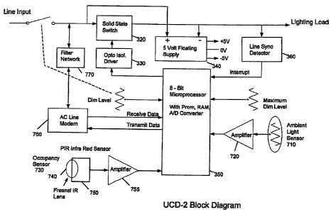
>> Figure 7 shows a block diagram of an energy savings device UCD-2
according to a second embodiment, and Figure 8 shows a schematic circuit
diagram of the energy savings device UCD-2 according to the second
embodiment. The energy savings device UCD-2 according to the second
embodiment provides all of the functions of the first embodiment, along with
extra functions. The UCD-2_includ.es an occupancy sensor, an ambient light
sensor, and an AC line modem for remote communications to a central energy
management system, for example. The UCD-2 provides a more robust energy
savings function than the UCD according to the first embodiment.
goo"s~ As shown in Figure 7, an ambient light sensor unit 710 of the second
embodiment provides the capability to adjust the dimming level for constant
level
illumination during day/night ambient illumination variailces. Referring also
to
Figure 8, the ambient light sensor unit 710 includes a photo-resistor R19 with
amplifier 720, which provides a stable indication of the total ambient
illumination
via a signal AMBLITE provided to port 1 of the microprocessor U2. The
microprocessor U2 adjusts the dimming level to maintain this total ambient
-42-
CA 02528061 2005-12-02
WO 2004/110107 PCT/US2004/017407
illumination level. For example, during a cloudy day, if the clouds break
during
the afternoon and thus the light through windows of an office increases, this
results in an increase in the illumination level picked up by the ambient
light
sensor unit 710. Accordingly, the microprocessor U2 will adjust the load
current
waveform to provide a slightly dimmer signal than what was previously provided
(during the cloudy period), so as to maintain a stable ambient illumination
for the
office.
[00119] Referring to Figure 7 , the occupancy sensor unit 730 of the second
embodiment provides the capability to sense movement within an illumination
area. The occupancy sensor unit 730 is configured to provide a signal
indicative
of no movement to the microprocessor U2 if no movement is sensed after an
extended interval of time (e.g.; IS minutes or more). 'Upon receipt of the "no
movement" signal from the occupancy sensor unit 730, the microprocessor U2
turns the light fixture off, in order to save energy. Similarly, illumination
to a
preset level is restored if movement occurs, such as when a person walks into
a
room. Referring to Figure 8, the occupancy sensor unit 730 according to a
preferred implementation includes a passive infrared sensor 750 with a
multifaceted (Fresnel) lens 740 in front of a pyroelectric transducer. For
example, a Murata IRA-E710ST0 may be utilized as the motion.detector for the
-43-
CA 02528061 2005-12-02
WO 2004/110107 PCT/US2004/017407
occupancy sensor unit 730. The lens 740 focuses infrared energy trom a
multitude of narrow, discrete beams or cones. As a warm body moves across the
field of view of the detector, the transducer output has peaks and valleys
which
are amplified, thereby providing an indication that movement is occurring.
This
results in a signal MOTDET that is indicative of movement being provided to
the
microprocessor U2.
0~ Referring to Figure 7, the AC line modem 760 of the second embodiment
enables bi-directional communications with an energy management unit, such as
with a centralized_energy management system (EMS). In one implementation
shown in Figure 8, the AC line modem is implemented as a line modem
TDA5051 component. The EMS has the capability to remotely control some or
all dimming functions and modes including turn off illumination (via signal
PWRDWN provided to microprocessor U2), set dimming level, and verify
occupancy sensor status (possible burglar alarm function). The EMS is
preferably a standard personal computer with external AC line modem connected
to a serial port. Software running under an operating system, such as the
Windows' operating system, maintains the status of all units within a local
area.
The AC line modem 760 functions by modulating a 200 KHz signal onto the AC
power line via a filter network 770 that includes an inductor L1 and a
capacitor
-44-
CA 02528061 2005-12-02
WO 2004/110107 PCT/US2004/017407
C4 (see Figure 8), in one possible implementation of the second embodiment.
The EMS can communicate with a wide area of dimming units that are on a
common AC line step down transformer, for example. Each dimming unit
carries a unique address to facilitate a mufti-drop communications network via
the power lines.
~oo,z,~ In a third embodiment, unlike the "loaded" second embodiment, only the
ambient Iight sensor unit of the second embodiment is provided along with the
features of the first embodiment.
~oo,zz~ In a fourth embodiment, only the occupancy sensor unit of the second
embodiment is provided along with the features of the first embodiment.
[00,23] In a fifth embodiment, only the AC line modem of the second embodiment
is provided along. with the features of the first embodiment. In another
possible
implementation, both the occupancy sensor unit and the AC line modem (but not
the ambient light sensor) of the second embodiment are utilized along with the
features of the first embodiment. In yet another possible implementation, both
the AC line modern and the ambient light sensor (but not the occupancy sensor
unit) are utilized along with the features of the first embodiment. In still
yet
another possible implementation, both the occupancy sensor unit and the
ambient
-45-
CA 02528061 2005-12-02
WO 2004/110107 PCT/US2004/017407
light sensor (but not the AC line modem) are utilized along with the reatures
or
the first embodiment.
~oo,2a~ A sixth embodiment of the invention includes all of the features
described
above with respect to the second embodiment, as wwell as a remote control
function. The remote control function allows a user to set a light level by a
remote control unit, without having to go to a switch box on a wall. By
pointing
the remote control unit in a direction of the switch box, and by enabling a
button
on the remote control unit, a signal is picked up by an element (e.g.,
infrared
sensor, IR sensor) on the switch box, similar to a television remote control
unit,
whereby a room light level is either increased or decreased depending on the
user's selection on the remote control unit. The remote control function can
also
be used with any of the other embodiments described above.
[00,25] A seventh embodiment of the invention is described herein with respect
to
Figures 9 and 10. The seventh embodiment is directed to a master/follower
control system, whereby a master unit controls one or more reactive loads, and
whereby at least one follower unit coupled to the master unit responds exactly
the
same as the master unit to control loads coupled to each follower' unit. The
master/follower control system according to the seventh embodiment provides
for
modular flexibility for different sizes of facilities. Figure 9 shows a
schematic
-46-
CA 02528061 2005-12-02
WO 2004/110107 PCT/US2004/017407
circuit diagram of a master unit 900. Figure 10 shows a schematic circuit
diagram of a follower unit 1000 that is controlled by the master unit 900 of
Figure 9.
~oo,zs~ The seventh embodiment includes a conduction angle phase switching
circuit connected in parallel with a reactive load, an AC power source for
switching power across the load, and a line switching circuit for enabling the
application of AC power to the load through the phase switching circuit.
~00,27j In the seventh embodiment, an ambient, light sensor 910 is provided
for
generating a Iight control signal indicative of the amount of ambient light
present
in a particular location. Coupled to the light sensing circuit is a phase
angle
conduction control circuit, which generates and applies to a control terminal
of
the phase switching circuit a phase control signal to control the phase angle
conduction time of the phase switching circuit, based on the amount of ambient
light measured by the light sensing circuit, in order to maintain a
substantially
constant lighting level. In Figure 9, the microprocessor U3 functions as the
phase angle conduction control circuit.
~oo,zs~ Integrated with the phase angle conduction control circuit is an RC
filter
circuit which gradually increases the phase angle conduction time switching
circuit from zero, or from a predetermined minimum value, to a steady state
-47-
CA 02528061 2005-12-02
WO 2004/110107 PCT/US2004/017407
phase angle conduction time based on the ambient light conamcns JCU~~u ~y «~,.
light sensing circuit, after power enabling by the line switching circuit.
[00129] Referring to Figure 9, the master unit includes a line switch SW 1
connected in series with an AC power source between a hot (black) and a
neutral
(white) power line. Connected in series between the hot and neutral power
lines
is an reactive load (e.g., fluorescent lamp), and a phase angle control
switching
device that includes SCRs Ql and Q2 and an opto-isolated triac U1 for driving
the SCRs (see discussion with respect to the first embodiment).
~ Also shown in Figure 9 is the microprocessor U3, which receives a line
sync signal from a bridge circuit Dl that is coupled to the hot and neutral
lines.
Based on the line sync signal, and based on the setting of the potentiometer
and
switch SW1, the microprocessor U3 provides control signals to the opto-
isolated
triac Ul, as well as to follower units coupled to the master unit via pulse
width
modulated (PWM) signaling.
[00131] Figure 10 shows the elements of a follower unit 1000,, which receives
the
PWM control signals from the master unit, and which controls one or more loads
connected to the follower unit based on on/off switching of its active element
(SCRs Q1, Q2, and opto-isolated triac U1) via those control signals.
-48-
CA 02528061 2005-12-02
WO 2004/110107 PCT/US2004/017407
(00132] Different embodiments of the present invention have been described
according to the present invention. Many modifications. and variations may be
made to the techniques and structures described and illustrated herein without
departing from the spirit and scope of the invention. Accordingly, it should
be
understood that the apparatuses described herein are illustrative only and are
not
limiting upon the scope of the invention. With the use of an energy savings
device according to an embodiment of the invention, it is possible to achieve
a
50% or more energy savings, while not adversely affecting the perceived amount
of light by users.
[00133) Also, the above-described embodiments of the present invention are
capable of providing dimming for electronic ballast fluorescent fixtures,
using the
same electronics and software as those described earlier with. respect to
magnetic
ballast fluorescent fixtures. Tests performed by the inventors showed a
dimming
capability for several different types of electronic ballast fluorescent
fixtures,
without any noticeable flickering. Therefore, an apparatus and method
according
to different embodiments of the present invention can be used to control
resistive,
inductive, and/or capacitive loads.
-49-