Note: Descriptions are shown in the official language in which they were submitted.
CA 02528091 2005-12-02
1
DESCRIPTION
ELECTRODE FOR DISCHARGE SURFACE TREATMENT, MANUFACTURING
METHOD AND EVALUATION METHOD FOR ELECTRODE FOR DISCHARGE
SURFACE TREATMENT, DISCHARGE SURFACE TREATMENT APPARATUS,
AND DISCHARGE SURFACE TREATMENT METHOD
TECHNICAL FIELD
The present invention relates to an electrode for
discharge surface treatment that is used for discharge
surface treatment for causing pulsed electric discharge
between an electrode for discharge surface treatment, which
consists of a green compact obtained by compression-molding
powder of metal, a metallic compound, or ceramics, and a
work piece and forming, using discharge energy of the
electric discharge, a film consisting of an electrode
material or a substance generated by reaction of the
electrode material due to the discharge energy on a surface
of the work piece and a manufacturing method and an
valuation method for the electrode for discharge surface
treatment. The present invention also relates to a
discharge surface treatment apparatus and a discharge
surface treatment method using the electrode for discharge
surface treatment.
BACKGROUND ART
Welding and thermal spraying have been conventionally
used for surface treatment for a turbine blade and the like
of a gas turbine engine for an aircraft because it is
necessary to coat or build up a material having strength
and lubricity under a high-temperature environment. With
the welding and thermal spraying, a film of a material
containing Cr (chrome) or Mo (molybdenum), which is known
CA 02528091 2005-12-02
2
to be oxidized into oxide under the high-temperature
environment and show lubricity, as a base is built up thick
on a work piece (hereinafter, "work"). The welding refers
to a method of melting and depositing a material for a
welding rod with electric discharge between the work and
the welding rod. The thermal spraying refers to a method
of bringing a metal into a fused state and spraying the
metal material on the work to form a film.
However, both the welding and the thermal spraying are
manual machining and require skill. Thus, there is a
problem in that it is difficult to automate the machining
and cost for the machining increases. In particular, since
the welding is a method of concentrating heat in a work,
there is a problem in that weld crack tends to occur when a
thin material is treated and when a fragile material, for
example, a single crystal alloy or a directional control
alloy like a directionally solidified alloy is treated.
As a technology for solving such problems, a method of
coating a surface of a metal material used as a work with
submerged discharge is proposed. For example, a first
conventional technology discloses a technology for
performing submerged discharge using an electrode material
containing a component of a film to be formed on a work as
primary machining and, then, applying re-melting discharge
machining to the electrode material deposited on the work
using a separate copper electrode or an electrode like
graphite that is not worn much (see, for example, Patent
Document 1). According to the conventional technology, a
coating layer having satisfactory hardness and adhesion is
obtained for a steel material used as the work. However,
it is difficult to form a coating layer having strong
adhesion on a surface of a sintered material like a
cemented carbide. The method requires two steps consisting
CA 02528091 2005-12-02
3
of the first machining for forming a film and the second
machining for subjecting the film to re-melting discharge
to cause the film to adhere to the work. Thus, there is a
problem in that the treatment is complicated.
A second conventional technology discloses a
technology for forming a hard ceramic film on a metal
surface only through a change in a discharge electrical
condition without replacing an electrode in such treatment
for forming a film at two steps of machining (see, for
example, Patent Document 2). In the second conventional
technology, ceramic powder to be used as a material for
forming an electrode compression-molded at an extremely
high pressure of 10 t/cmz and pre-sintered to have density
of 50o to 900 of a logical density is used as an electrode.
In a third conventional technology, with a material
forming hard carbide like Ti (titanium) as an electrode,
electric discharge is caused between the electrode and a
metal material used as a work. Consequently, a strong hard
film is formed on a metal surface without a step of re-
melting that is required in the first and the second
conventional technologies (see, for example, Patent
Document 3). The technology utilizes a phenomenon in which
the electrode material worn by electric discharge reacts
with C (carbon), which is a component in a machining fluid,
to generate TiC (titanium carbide). When a green compact
electrode of metal hydride like TiHz (titanium hydride) is
used to cause electric discharge between the green compact
electrode and a metal material used as a work, it is
possible to form a hard film with satisfactory adhesion
faster than using the metal material such as Ti. Moreover,
when a green compact electrode formed by mixing hydride
such as TiH2 with other metals or ceramics is used to cause
electric discharge between the green compact electrode and
CA 02528091 2005-12-02
4
a metal material used as a work, it is also possible to
quickly form a hard film having various characteristic like
high hardness and abrasion resistance.
In a fourth conventional technology, ceramic powder is
compression-molded, a green compact electrode with high
strength is manufactured by pre-sintering, and a film of a
hard material such as TiC is formed by electric discharge
surface treatment using the electrode (see, for example,
Patent Document 4). As an example of the fourth
conventional technology, manufacturing of an electrode for
discharge surface treatment (hereinafter simply referred to
as electrode as well) consisting of powder obtained by
mixing tungsten carbide (WC) powder and cobalt (Co) powder
is explained. A green compact obtained by mixing and
compression-molding the WC powder and the Co powder may be
simply obtained by mixing and compression-molding the WC
powder and the Co powder. It is more desirable to
compression-molding the WC powder and the Co powder after
mixing wax therein because moldability of the green compact
is improved. However, since the wax is an insulating
material, if a large quantity of the wax remains in the
electrode, dischargeability is deteriorated because an
electrical resistance of the electrode increases. Thus, it
is necessary to remove the wax. The wax is removed by
putting the green compact in a vacuum furnace and heating
the green compact. At this point, if heating temperature
is too low, the wax cannot be removed. If heating
temperature is too high, the wax changes to soot to
deteriorate purity of the electrode. Thus, it is necessary
to keep heating temperature at temperature equal to or
higher than temperature at which the wax is melted and
temperature not more than temperature at which the wax is
resolved to be soot. Subsequently, the green compact in
CA 02528091 2005-12-02
the vacuum furnace is heated by a high-frequency coil or
the like to give strength durable against machining and
sintered not to be hardened excessively, for example, until
the green compact becomes as hard as chalk. Such sintering
5 is referred to as pre-sintering. In this case, carbides
are mutually bonded in a contact portion thereof. However,
since sintering temperature is relatively low and is not as
higher as temperature for real sintering, the bonding is
weak. When discharge surface treatment is performed with
the electrode with high strength sintered by pre-sintering
in this way, it is possible to form a dense and homogeneous
film on a surface of a work.
Patent Document l: Japanese Patent Application Laid-
Open No. H5-148615
Patent Document 2: Japanese Patent Application Laid-
Open No. H8-300227
Patent Document 3: Japanese Patent Application Laid-
Open No. H9-192937
Patent Document 4: International Publication No.
99/58744 Pamphlet
As described in the third and the fourth conventional
technologies, it is possible to form a dense hard film
according to discharge surface treatment using an electrode
obtained by sintering a green compact. However, when a
thick film is formed with such discharge surface treatment,
there is a problem in that there is a significant
difference in characteristics of electrodes even if the
electrodes are manufactured as disclosed in the fourth
conventional technologies. In addition, it is difficult to
form a dense film.
As one possible cause of the difference is a
difference in distribution of particle diameters of powders
of a material of the electrodes. This is because, if there
CA 02528091 2005-12-02
6
is a difference in distribution of particle diameters of
powders with which the electrodes are manufactured, since a
hardening condition is different for each of the electrodes
even if the electrodes are pressed at the same pressure and
formed, a difference in strength of the electrodes occurs
finally. Another possible cause of the difference in
characteristics of the electrodes is a change of a material
(a component) of the electrodes that is performed to change
a material of a film to be formed on a work. This is
because, when a material of the electrodes is changed,
strength of the electrodes differs from strength of the
electrodes before the change because of a difference in a
physical property value.
It is also known that, when a thin film is formed
according to the discharge surface treatment, a way of
supply of a material from the electrode side and a way of
melting of the material supplied on a surface of a work and
bonding of the material with a work material affect film
performance most. One index affecting the supply of an
electrode material is hardness of the electrode. For
example, in the fourth conventional technology, hardness of
the electrode for discharge surface treatment is set to
hardness that is strength durable against machine machining
and is not too high (e.g., hardness equivalent to that of
chalk). With the electrode having such hardness, supply of
the electrode material by electric discharge is controlled
and the material supplied is sufficiently melted. Thus, it
is possible to form a hard ceramic film on the surface of
the work.
The hardness equivalent to that of chalk, which is the
index of hardness of the electrode for discharge surface
treatment, is extremely ambiguous. There is also a problem
in that a difference of thick films formed on the surface
CA 02528091 2005-12-02
7
of the work is caused by characteristics such as hardness
of the electrode. When a material and a size of powder to
be an electrode are changed, a condition for formation of
the electrode is different. Therefore, there is a problem
in that a step of changing a large number of conditions for
formation of the electrode to perform formation tests for a
film and deciding a formation condition suitable for use of
the material as the electrode for discharge surface
treatment is required for each material of the electrode.
In other words, there is a problem in that tests for
obtaining formation conditions for the electrode for
forming a satisfactory film have to be performed a number
of times equivalent to types of materials forming the
electrodes, which takes a lot of time and labor. Besides,
even if electrodes are manufactured by the same
manufacturing method using powder of the same material, a
volume of the powder changes depending on a season
(temperature and humidity). Thus, as in the case of the
change of the material, powders with different volumes have
to be actually machined to form films and evaluate the
electrodes. This takes a lot of time and labor.
Under the present circumstances, the conventional
discharge surface treatment mainly aims at formation of a
hard film, in particular, formation of a hard film at
temperature close to the room temperature to form a film
containing hard carbide as a main component. With this
method, only a thick film of about 10 micrometers can be
formed and it is impossible to increase thickness of a film
to be equal to or larger than several tens micrometers.
Conventionally, a material easily forming carbide is
contained in an electrode at a high rate. For example, if
a material such as Ti is contained in an electrode, a
chemical reaction is caused by electric discharge in oil.
CA 02528091 2005-12-02
8
As a result, a hard carbide TiC is obtained as a film.
This is because, as surface treatment progresses, a
material of a surface of a work changes from a steel
material (when the material is machined into a steel
material) to TiC, which is ceramics, and characteristics
like thermal conduction and a melting point changes.
However, according to an experiment performed by the
inventors, the inventors have found that it is possible to
increase thickness of a film by adding a material not
forming carbide or less easily forming carbide to
components of an electrode material. This is because a
quantity of materials not changing to carbide and remaining
in the film in a metal state increases by adding the
material to the electrode. It has been found that
selection of an electrode material has a significant
meaning in thickly building up a film. In this case, the
film to be formed still has hardness, density, and
uniformity. However, as described above, the conventional
discharge surface treatment mainly aims at formation of a
film that shows hardness at temperature close to the room
temperature such as TiC and WC. The conventional discharge
surface treatment does not pay attention to formation of a
dense and relatively thick film (a thin film in an order of
100 micrometers or more) that has lubricity under a high-
temperature environment like an application to a turbine
blade of a gas turbine engine for an aircraft. Thus, there
is a problem in that it is impossible to form such a thick
film.
On the other hand, in the second conventional
technology, an electrode obtained by compression-molding
ceramic powder to be a material forming an electrode at an
extremely high pressure of 10 t/cm2 and pre-sintering the
material to have density of 50o to 900 of a logical density
CA 02528091 2005-12-02
9
is used. This is because, for example, (1) since it is an
object of the technology to form a thin hard film, a film
is strengthened more as an electrode is made harder, and
(2) since a main component of a material is ceramics,
pressure in compression-molding ceramic powder forming the
electrode may be increased. However, when a dense metal
film is formed according to the discharge surface treatment,
it is impossible to use an electrode manufactured by the
method described in the second conventional technology.
This is because, when metal powder is pressed at extremely
high pressure of 10 t/cmz as described in the second
conventional technology, since an electrode is hardens, it
is impossible to form a film according to the discharge
surface treatment. If the discharge surface treatment is
performed with such an electrode, this results in die
sinking for shaving a surface of a work. In the second
conventional technology, since ceramic powder is used, no
problem is caused even if the ceramic powder is pressed at
the high pressure described above to manufacture an
electrode for discharge surface treatment. However, the
condition cannot be directly applied to an electrode for
discharge surface treatment consisting of metal powder. A
manufacturing method for an electrode for discharge surface
treatment for forming a dense metal thick film according to
the discharge surface treatment has not been conventionally
known.
The present invention has been devised in view of the
circumstances and it is an object of the present invention
to obtain an electrode for discharge surface treatment that
is capable of easily forming a dense thick film on a work
piece according to a discharge surface treatment method.
It is another object of the present invention to
obtain an electrode for discharge surface treatment that
CA 02528091 2005-12-02
~O
can form a thick film having lubricity under a
high-temperature environment in discharge surface
treatment. It is still another object of the present
invention to obtain an evaluation method for an electrode
for discharge surface treatment for evaluating whether it
is possible to use the electrode for discharge surface
treatment in formation of a film.
It is still another obj ect of the present invention
to obtain an electrode for discharge surface treatment that
causes, in discharge surface treatment using metal powder
as a green compact electrode, the green compact electrode
to perform stable electric discharge without decreasing
surface roughness and deposit a thick film.
It is still another obj ect of the present invention
to obtain a discharge surface treatment apparatus that uses
the electrode for discharge surface treatment and a method
for the discharge surface treatment apparatus.
BACKGROUND ART
To achieve the above objects, an electrode for
discharge surface treatment according to an aspect of the
present invention is used for discharge surface treatment
for causing, with a green compact obtained by
compression-molding powderof metal, a metallic compound,
or ceramics as an electrode, electric discharge between
CA 02528091 2005-12-02
1~
the electrode and a work piece in a machining fluid or in
an air and forming, using discharge energy of the electric
discharge, a film consisting of an electrode material or
a substance generated by reaction of the electrode material
due to the discharge energy on a surface of the work piece,
wherein the powder has an average particle diameter of 5
micrometer to 10 micrometers and contains 40 volume percent
or more of a component not forming or less easily forming
carbide as a component for forming the film on the work
piece and the electrode is formed to have hardness in a
range of B to 8B in hardness according to a pencil scratch
test for a coating film.
An electrode for discharge surface treatment
according to another aspect of the present invention is
Z5 used for discharge surface treatment for causing, with a
green compact obtained by compression-molding powder of
metal or a metallic compound as an electrode, electric
discharge between the electrode and a work piece in a
machining fluid or in an air and forming, using discharge
energy of the electric discharge, a film consisting of an
electrode material or a substance generated by reaction
of the electrode material due to the discharge energy on
a surface of the work piece, wherein when an average particle
diameter in a logarithmic scale in a semilogarithmic
correlation diagram of an average particle diameter and
CA 02528091 2005-12-02
compressionstrengthis0.05micrometer,lmicrometer,and
3 micrometer, compression strength of the electrode is
lower than a line that joins values 160 MPa, 100 Mpa, and
50 Mpa.
An electrode for discharge surface treatment
according to another aspect of the present invention is
used for discharge surface treatment for causing, with a
greencompactobtained bycompression-molding anelectrode
material that is powder of metal or a metallic compound
as an electrode, electric discharge between the electrode
and a work piece in a machining fluid or in an air and forming,
using discharge energy of the electric discharge, a film
consisting of the electrode material or a substance
generated by reaction of the electrode material due to the
discharge energy on a surface of the work piece, wherein
a volume ratio of the electrode material in a volume of
the electrode is within a specific range between 25o to
65 o depending on a distribution of particle diameter, and
the volume ratio is adjusted within the range such that
the volume ratio is high when a distribution of particle
diameter is wide and the volume ratio is low when a
distribution of particle diameter is narrow.
An electrode for discharge surface treatment
according to another aspect of the present invention is
used for discharge surface treatment for causing, with a
CA 02528091 2005-12-02
~l
green compact obtained by compression-molding powder of
metal or a metallic compound as an electrode, electric
discharge between the electrode and a work piece in a
machining fluid or in an air and forming, using discharge
energy of the electric discharge, a film consisting of an
electrode material or a substance generated by reaction
of the electrode material due to the discharge energy on
a surface of the work piece, wherein a thermal conductivity
is not more than 10 W/mK.
Moreover, to achieve the above objects, a discharge
surface treatment method according to another aspect of
the present invention of causing, with a green compact
obtained bycompression-molding powderofmetal,a metallic
compound, or ceramics as an electrode, electric discharge
between the electrode and a work piece in a machining fluid
or in an air and forming, using discharge energy of the
electric discharge, a film consisting of an electrode
material or a substance generated by reaction of the
electrode material due to the discharge energy on a surface
of the work piece, including preparing a powder that has
an average particle diameter of 5 micrometer to 10
micrometers and contains 40 volume percent or more of a
component not forming or less easily forming carbide as
a component for forming the film on the work piece and with
a hardness in a range of B to 8B in hardness according to
CA 02528091 2005-12-02
a pencil scratch test for a coating film, and using an
electrode made of the powder to form the film.
A discharge surface treatment method according to
another aspect of the present invention of causing, with
a green compact obtained by compression-molding powder of
metal or a metallic compound as an electrode, electric
discharge between the electrode and a work piece in a
machining fluid or in an air and forming, using discharge
energy of the electric discharge, a film consisting of an
electrode material or a substance generated by reaction
of the electrode material due to the discharge energy on
a surface of the work piece, including when an average
particle diameter in a logarithmic scale in a
semilogarithmiccorrelation diagramofanaverageparticle
diameter and compression strength is 0.05 micrometer, 1
micrometer, and 3 micrometer, using an electrode having
a compression strength of the electrode is lower than a
line that joins values 160 MPa, 100 Mpa, and 50 Mpa to form
the film.
A discharge surface treatment method according to
another aspect of the present invention of causing, with
a green compact obtained by compression-molding an
electrode material that is powder of metal or a metallic
compound as an electrode, electric discharge between the
electrode and a work piece in a machining fluid or in an
CA 02528091 2005-12-02
air and forming, using discharge energy of the electric
discharge, a film consisting of the electrode material or
a substance generated by reaction of the electrode material
due to the discharge energy on a surface of the work piece,
including using an electrode having a volume ratio of the
electrode material in a volume of the electrode is within
a specific range between 25o to 65o depending on a
distribution of particle diameter, and the volume ratio
is adjusted within the range such that the volume ratio
is high when a distribution of particle diameter is wide
and the volume ratio is low when a distribution of particle
diameter is narrow.
A discharge surface treatment method according to
another aspect of the present invention of causing, with
a green compact obtained by compression-molding powder of
metal or a metallic compound as an electrode, electric
discharge between the electrode and a work piece in a
machining fluid or in an air and forming, using discharge
energy of the electric discharge, a film consisting of an
electrode material or a substance generated by reaction
of the electrode material due to the discharge energy on
a surface of the work piece, including using an electrode
having a thermal conductivity not more than 10 W/mK to form
the film.
Moreover, to achieve the above objects, a discharge
CA 02528091 2005-12-02
a E
surface treatment apparatus according to another aspect
of the present invention has an electrode consisting of
a green compact obtained by compression-molding powder of
metal, a metallic compound, or ceramics and a work piece
on which a film is formed, the electrode and the work piece
being arranged in a machining fluid or in an air, generates
a pulsed electric discharge between the electrode and the
work piece using a power supply apparatus electrically
connected to the electrode and the work piece, and forms,
using discharge energy of the electric discharge, a film
consisting of an electrode material or a substance
generated by reaction of the electrode material due to the
discharge energy on a surface of the work piece, wherein
the electrode molds powder with an average particle
diameter of 5 to 10 micrometers containing 40 volume percent
or more of a component not forming or less easily forming
carbide as a component for forming the film on the work
piece and a component not forming or less easily forming
carbide to have hardness in a range of B to 8B in hardness
according to a pencil scratch test for a coating film.
A discharge surface treatment apparatus according
to another aspect of the present invention has an electrode
consisting of a green compact obtained by
compression-molding powderof metalora metallic compound
and a work piece on which a film is formed, the electrode
CA 02528091 2005-12-02
and the work piece being arranged in a machining fluid or
in an air, generates a pulsed electric discharge between
the electrode and the work piece using a power supply
apparatus electrically connected to the electrode and the
work piece, and forms, using discharge energy of the
electric discharge, a film consisting of an electrode
material or a substance generated by reaction of the
electrode material due to the discharge energy on a surface
of the work piece, wherein when an average particle diameter
in a logarithmic scale in a semilogarithmic correlation
diagram of an average particle diameter and compression
strength is 0 . 05 micrometer, 1 micrometer, and 3 micrometer,
compression strength of the electrode is lower than a line
that joins values 160 MPa, 100 Mpa, and 50 Mpa.
A discharge surface treatment apparatus according
to another aspect of the present invention has an electrode
consisting of a green compact obtained by
compression-molding powderof metalorametalliccompound
and a work piece on which a film is formed, the electrode
and the work piece being arranged in a machining fluid or
in an air, generates a pulsed electric discharge between
the electrode and the work piece using a power supply
apparatus electrically connected to the electrode and the
work piece, and forms, using discharge energy of the
electric discharge, a film consisting of an electrode
CA 02528091 2005-12-02
1 .; L1
material or a substance generated by reaction of the
electrode material due to the discharge energy on a surface
of the work piece, wherein, in the electrode, a volume ratio
of the electrode material in a volume of the electrode is
25% to 650, and the volume ratio is adjusted within the
range such that the volume ratio is high when a distribution
of particle diameter is wide and the volume ratio is low
when a distribution-of particle diameter is small.
A discharge surface treatment apparatus according
to another aspect of the present invention has an electrode
consisting of a green compact obtained by
compression-molding powder of metalora metalliccompound
and a work piece on which a film is formed, the electrode
and the work piece being arranged in a machining fluid or
in an air, generates a pulsed electric discharge between
the electrode and the work piece using a power supply
apparatus electrically connected to the electrode and the
work piece, and forms, using discharge energy of the
electric discharge, a film consisting of an electrode
material or a substance generated by reaction of the
electrode material due to the discharge energy on a surface
of the work piece, wherein the electrode has a thermal
conductivity not more than 10 W/mK.
BRIEF DESCRIPTION OF DRAWINGS
CA 02528091 2005-12-02
Fig. 1 is a schematic diagram of discharge surface
treatment performed by a discharge surface treatment
apparatus;
Fig. 2 is a flowchart of a process for manufacturing
an electrode to be used in discharge surface treatment;
Fig. 3 is a schematic sectional view of a state of
a molding device at the time when powder is molded;
Fig. 4A is a graph of a voltage waveform of a voltage
applied between an electrode for discharge surface
treatment and a work at the time of electric discharge;
Fig. 4B is a graph of a current wave form of a current
flowing in the discharge surface treatment apparatus at
the time of electric discharge;
Fig. 5 is a graph of a relation between an amount
of Co and a film thickness according to a change in the
amount of Co in an electrode for discharge surface treatment
manufactured by changing an amount of Co powder mixed in
Cr3C2 powder;
Fig. 6 is a graph of a state of formation of a film
with respect to a machining time at the time when a material
not forming carbide or a material less easily forming
carbide is not contained in an electrode for discharge
surface treatment;
Fig. 7 is a photograph of a film that is formed when
dischargesurfacetreatmentisperformed using anelectrode
CA 02528091 2005-12-02
.1 l C
with a Co content of 70 volume percent;
Fig. 8 is a graph of a state of thick film formation
at the time when hardness of an electrode for discharge
surface treatment with a volume ratio of Cr3Cz 300 - Co
70o is changed;
Fig. 9 is a photograph of a laboratory device for
measuring compression strength of an electrode;
Fig. 10 is a graph of a relation between compression
strength of an electrode and a film thickness;
Fig. 11 is a graph of a relation between an average
particlediameterandcompression strengthof anelectrode
that is capable of depositing a thick film;
Fig. 12 is a graph of a relation between a film
thickness formed on a surface of a work and a thermal
conductivity of an electrode for discharge surface
treatment at the time when discharge surface treatment is
performed usingelectrodesfordischargesurfacetreatment
with different thermal conductivities;
Fig. 13A is a schematic diagram of a method of judging
a quality of an electrode according to a film formation
test;
Fig. 13B is a schematic diagram of a method of judging
a quality of an electrode according to a film formation
test; and
Fig. 13C is a schematic diagram of a method of judging
CA 02528091 2005-12-02
_1- ~ of
a quality of an electrode according to a film formation
test.
CA 02528091 2005-12-02
18
BEST MODES) FOR CARRYING OUT THE INVENTION
Exemplary embodiments of an electrode for discharge
15 surface treatment, a manufacturing method and an evaluation
method for the electrode for discharge surface treatment, a
discharge surface treatment apparatus, and a discharge
surface treatment method according to the present invention
are explained in detail below.
20 First embodiment
First, a discharge surface treatment method and an
apparatus therefor used in the present invention are
schematically explained. Fig. 1 is a diagram schematically
showing discharge surface treatment in a discharge surface
25 treatment apparatus. A discharge surface treatment
apparatus 1 includes a work piece (hereinafter, "work") Z1
on which a film 14 is formed, an electrode for discharge
surface treatment 12 for forming the film 14 on the surface
of the work 11, and a power supply for discharge surface
30 treatment that supplies a voltage to both the work 11 and
the electrode for discharge surface treatment 12 to cause
arc discharge between both the work 11 and the electrode
for discharge surface treatment 12 electrically connected.
CA 02528091 2005-12-02
19
When the discharge surface treatment is performed in a
liquid, a work tank is further provided and the work 11 and
a portion of the electrode for discharge surface treatment
12 opposed to the work 11 are filled with a machining fluid
15 such as oil. When the discharge surface treatment is
performed in the air, the work 11 and the electrode for
discharge surface treatment 12 are placed in a treatment
atmosphere. Note that, in an example shown in Fig. 1 and
explained below, the discharge surface treatment is
performed in a machining fluid. In the following
explanation, the electrode for discharge surface treatment
is simply called an "electrode". Moreover, in the
following explanation, a distance between opposed surfaces
of the electrode for discharge surface treatment 12 and the
work 11 is referred to as a distance between electrodes.
A discharge surface treatment method in the discharge
surface treatment apparatus 1 having such a constitution is
explained below. The discharge surface treatment is
performed by, for example, with the work 11 on which the
film 14 is desired to be formed set as an anode and the
electrode for discharge surface treatment 12, which is
obtained by molding powder with an average particle
diameter of 10 nanometers to several micrometers such as
metal and ceramics, serving as a supply source of the film
14 set as a cathode, causing electric discharge between the
anode and the cathode while controlling the distance
between electrodes with a not-shown control mechanism to
prevent both the electrodes from coming into contact with
each other in the machining fluid 15.
When electric discharge occurs between the electrode
for discharge surface treatment 12 and the work 11, part of
the work and the electrode 12 melt by the heat generated
due to the electric discharge. When a binding force among
CA 02528091 2005-12-02
particles of the electrode 12 is weak, a part (hereinafter,
electrode particles) 21 of the electrode 12 melted is
separated from the electrode l2 by air blast and a static
electric force caused by the electric discharge and moves
5 to the surface of the work 11. When the electrode
particles 21 reach the surface of the work 11, the
electrode particles 21 solidify again and change to the
film 14. A part of the electrode particles 21 reacting
with components 22 in the machining fluid 15 or the air
10 also forms the film 14 on the surface of the work 11. In
this way, the film 14 is formed on the surface of the work
11. However, when a binding force among particles of the
electrode 12 is strong, the electrode 12 is not stripped
off by air blast and a static electrical force due to the
15 electric discharge. Thus, it is impossible to supply an
electrode material to the work 11. In other words,
possibility of formation of a thick film according to the
discharge surface treatment is affected by supply of a
material from the electrode 12 side, melting of the
20 material supplied on the surface of the work 11 and a way
of bonding of the material with the material of the work 11.
Hardness of the electrode 12 affects the supply of an
electrode material.
An example of a method of manufacturing the electrode
for discharge surface treatment 12 used for the discharge
surface treatment is explained. Fig. 2 is a flowchart of a
process for manufacturing an electrode to be used in
discharge surface treatment. First, powder of metal,
ceramics, or the like having a component of the film 14
desired to be formed on the work 11 is ground (step Sl).
When the film 14 consists of a plurality of components,
powders of the respective components are mixed and ground
such that a desired ratio of the components is obtained.
CA 02528091 2005-12-02
21
For example, spherical powder of metal, ceramics, or the
like with an average particle diameter of several tens
micrometers circulated in the market is ground into powder
with an average particle diameter not more than 3
micrometers by a grinder like a ball mill apparatus. The
grinding may be performed in a liquid. However, in this
case, the liquid is evaporated to dry the powder (step S2).
In the powder after drying, particles are aggregated with
each other to form a large mass, and the large mass is
taken apart into pieces and sieved to sufficiently mix a
wax used at the next step and the powder (step S3). For
example, when a ceramic sphere or a metal sphere is placed
on a net of a sieve, on which the aggregated powder remain,
and the net is vibrated, the mass formed by aggregation is
taken apart by energy of the vibration and collision with
the sphere and passes through meshes of the net. Only the
powder passing through the meshes of the net is used at a
step described below.
The process of sieving performed at step S3 is
explained in detail below. In the discharge surface
treatment, a voltage applied between the electrode for
discharge surface treatment 12 and the work 11 to cause
electric discharge is usually in a range of 80 volts to 400
volts. When a voltage in this range is applied between the
electrode 12 and the work 11, a distance between the
electrode 12 and the work 11 during the discharge surface
treatment is set to about 0.3 millimeter. As described
above, it can be surmised that, in the discharge surface
treatment, the aggregated mass forming the electrode 12 may
leave the electrode 12 because of arc discharge caused
between both the electrodes while keeping a size of the
mass. If the size of the mass is not more than the
distance between electrodes (not more than 0.3 millimeter),
CA 02528091 2005-12-02
22
it is possible to cause the next electric discharge even if
the mass is present between the electrodes. Since electric
discharge occurs in places in a short distance from each
other, it is considered that electric discharge occurs in a
place where the mass is present and it is possible to crash
the mass into small pieces with thermal energy and an
explosive force of the electric discharge.
However, when the size of the mass forming the
electrode 12 is equal to or larger than the distance
between electrodes (equal to or larger than 0.3 millimeter),
the mass leaves from the electrode 12 because of electric
discharge while keeping the size and is deposited on the
work 11 or drifts in an interelectrode space filled with
the machining fluid 15 between the electrode 12 and the
work 11. When the large mass is deposited, since electric
discharge occurs in a place where a distance between the
electrode and the work 11 is small, electric discharge
concentrates in that place and cannot be caused in other
places. Thus, it is impossible to uniformly deposit the
film 14 on the surface of the work 11. Since the large
mass is too large, it is impossible to completely melt the
mass with heat of the electric discharge. Thus, the film
14 is so fragile as to be shaved by a hand. When the large
mass drifts in the interelectrode space, the electrode 12
and the work 11 are short-circuited so that an electric
discharge does not occur. In other words, to uniformly
form the film 14 and obtain stable electric discharge, a
mass equal to or larger than a distance between electrodes,
which is formed by aggregation of powder, must not be
present in the powder forming the electrode. The
aggregation of the powder is likely to occur in the case of
metal powder and conductive ceramics and is less likely to
occur in the case of nonconductive powder. The aggregation
CA 02528091 2005-12-02
23
of the powder is more likely to occur as an average
particle diameter of the powder is reduced. Therefore, to
prevent a harmful effect during the discharge surface
treatment due to a mass generated by such aggregation of
the powder, a step of sieving the aggregated powder at step
S3 is required. To that effect, in sieving the powder, it
is necessary to use meshes of a net smaller than the
distance between electrodes.
Thereafter, to make transmission of a pressure of
press to the inside of the powder better in the case of
press at a later step, wax like paraffin is mixed at a
weight ratio of to to loo as required (step S4). When the
powder and the wax are mixed, although it is possible to
improve moldability, since the periphery of the powder is
covered with a liquid again, the powder is aggregated by an
intermolecular force of the powder and a static electrical
force to form a large mass. Thus, the mass aggregated is
sieved again to be taken apart into pieces (step S5). A
way of sieving is the same as the method at step S3
described above.
Subsequently, powder obtained at step S5 is molded by
a compression press (step S6). Fig. 3 is a schematic
sectional view of a state of a molding device at the time
when powder is molded. A lower punch 104 is inserted from
a bottom of a hole formed in a die 105. Powder (a mixture
of the powders when the powders consist of a plurality of
components) sieved at step S5 is filled in a space formed
by the lower punch 104 and the die 105. Thereafter, an
upper punch 103 is inserted from a top of the hole formed
in the die 105. Pressure is applied from both sides of the
upper punch 103 and the lower punch 104 of the molding
device filled with such powder 101 by a pressurizer or the
like to compression-mold the powder 101. In the following
CA 02528091 2005-12-02
24
explanation, the powder 101 compression-molded is referred
to a green compact. In this case, the electrode 12 is
hardened when a press pressure is increased. The electrode
12 is softened when the press pressure is decreased. The
electrode 12 is hardened when a particle diameter of the
powder 101 of the electrode material is small. The
electrode 12 is softened when a particle diameter of the
powder 101 is large.
Thereafter, the green compact is taken out from the
molding device and heated in a vacuum furnace or a furnace
of a nitrogen atmosphere (step S7). In the case of heating,
the electrode 12 is hardened when a heating temperature is
raised and the electrode 12 is softened when a heating
temperature is lowered. It is also possible to lower an
electric resistance of the electrode 12 by heating the
green compact. Therefore, it is meaningful to heat the
green compact even when the powder is compression-molded
without mixing wax in the powder at step S4. Consequently,
bonding among the powders in the green compact progresses
and the electrode for discharge surface treatment 12 having
electrical conductivity is manufactured.
Note that, even when the grinding step at step S1 is
omitted, that is, when the powder with the average particle
diameters of several tens micrometers is directly used, or
when the sieving step at step S3 is omitted and the large
mass equal to or larger than 0.3 millimeter is mixed, it is
possible to mold the electrode for discharge surface
treatment 12. However, there is a problem in that the
electrode 12 has fluctuation in hardness, that is, hardness
on the surface is slightly high and hardness in the center
is low.
Powder with an average diameter not more than 3
micrometers of Co or Ni (Nickel), which is less easily
CA 02528091 2005-12-02
oxidized, an alloy or oxide of Co and Ni, or ceramics are
often circulated in the market. Thus, when such powder is
used, it is possible to omit the grinding step at step Sl
and the drying step at step S2.
5 Specific embodiments of the electrode for discharge
surface treatment manufactured by the method described
above are explained. In the first embodiment, when an
average particle diameter of powder forming an electrode is
5 micrometers to 10 micrometers, a relation among a ratio
10 of a material not forming carbide or a material less easily
forming carbide, hardness of the electrode, and thickness
of a film formed by the electrode is explained.
In the first embodiment, a result of testing,
concerning an electrode for discharge surface treatment
15 with a component of the material not forming carbide or a
material less easily forming carbide changed, changes in
hardness of the electrode and thickens of a film formed on
a work piece by the discharge surface treatment method is
described below. A material forming a basis of the
20 electrode for discharge surface treatment used for the test
was Cr3Cz (chromium carbide) powder. Co powder was added
to the Cr3Cz powder as the material not forming carbide or
the material less easily forming carbide. A volume of Co
to be added was changed between Oo and 80o and hardness of
25 the electrode for discharge surface treatment to be tested
was set to predetermined hardness. Note that the electrode
was manufactured from the Cr3Cz powder with a particle
diameter of 5 micrometers and the Co powder with a particle
diameter of 5 micrometers according to the flowchart in Fig.
2. At the grinding step of grinding powder at step Sl,
grinding was performed under a condition for obtaining
powder with a particle diameter of 5 micrometers. At the
mixing step of mixing powder with wax at step S4, wax with
CA 02528091 2005-12-02
26
2 to 3 weight percent was mixed. At the pressing step at
step S6, the powder was compression-molded at a press
pressure of about 100 MPa. At heating step at step S7, a
heating temperature was changed in a range of 400 °C to 800
°C. The heating temperature was set higher as a ratio of
the Cr3Cz powder was larger and was set lower as a ratio of
the Co powder was larger. This is because, whereas a
manufactured electrode tended to be fragile and easily
crumbled when heated at low temperature when the ratio of
the Cr3Cz powder was larger, strength of the electrode was
high even if a heating temperature was low when the ratio
of the Co powder was larger.
Note that a volume ratio (a volume percent) used in
this specification refers to a ratio of a value obtained by
dividing a weight percent of each of materials mixed by
density of each of the materials. Specifically, when a
plurality of materials are mixed, the volume ratio is a
ratio of volumes of the materials. When a material is an
alloy, a ratio of a value obtained by dividing a weight
percent of each of materials (metal elements) contained in
the alloy by density (specific gravity) of each of the
materials is set as the volume percent. In other words,
the volume percent is a value obtained by dividing a value,
which is obtained by dividing a weight percent of a target
component by density of the component, by a value obtained
by adding up values obtained by dividing weight percents of
respective components used in the electrode for discharge
surface treatment by densities of the components. For
example, a volume ratio (a volume percent) of Co powder in
a mixture of the Cr3C2 powder and the Co powder is
represented as the following expression.
Volume o of Co = Weight o of Co/Density of Co/(Weight o of
CA 02528091 2005-12-02
27
Cr3C2/Density of Cr3C2 + Weight o of Co/Density of Co)
From this expression, it goes without saying that,
when original specific gravities of materials mixed as an
alloy are close, volume percents of the materials are
substantially the same as weight percents thereof.
Discharge pulse conditions at the time of the
discharge surface treatment in the first embodiment are
explained. Figs. 4A and 4B are diagrams showing an example
of discharge pulse conditions at the time of the discharge
surface treatment. Fig. 4A shows a voltage waveform of a
voltage applied between an electrode for discharge surface
treatment and a work at the time of electric discharge.
Fig. 4B shows a current waveform of a current flowing to a
discharge surface treatment apparatus at the time of
electric discharge. As shown in Fig. 4A, a no-load voltage
ui is applied between both the electrodes at time to. A
current starts flowing between both the electrodes at time
tl after elapse of discharge delay time td and electric
discharge starts. The voltage at this point is a discharge
voltage ue and the current flowing at this point has a peak
current value ie. When supply of the voltage between both
the electrodes is stopped at time t2, the current stops
flowing. In other words, the electric discharge stops. In
this case, t2-tl refers to as a pulse width te. A voltage
with a voltage waveform at time t0 to t2 is repeatedly
applied between both the electrodes at intervals of a
quiescent time to. As shown in Fig. 4A, a pulsed voltage
is applied between the electrode for discharge surface
treatment 12 and the work 11. In this example, as the
discharge pulse conditions used at the time of the
discharge surface treatment, the peak current ie was set to
10 amperes, the discharge duration (the discharge pulse
CA 02528091 2005-12-02
28
width) to was set to 64 microseconds, the quiescent time
was set to 128 microseconds. In the test, the discharge
surface treatment was applied to the work 11 for fifteen
minutes using an electrode with an area 15 mm x 15 mm.
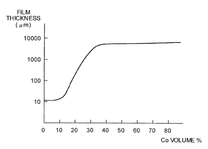
Fig. 5 is a graph of a relation between an amount of
Co and a film thickness according to a change in the amount
of Co in an electrode for discharge surface treatment
manufactured by changing an amount of the Co powder forming
carbide less easily mixed in the Cr3C2 powder that is
carbide. In Fig. 5, an abscissa indicates a volume
percentage of Co contained in the electrode for discharge
surface treatment and an ordinate indicates thickness (gym)
of a film formed on a work piece in a logarithmic scale.
When a film is formed based on the discharge pulse
conditions, thickness of a film formed on a work differs
depending on a volume percent of Co contained in a
manufactured electrode. According to Fig. 5, thickness of
about 10 micrometers at the Co content not more than 10
volume percent gradually increases from the Co content of
about 30 volume percent. When the Co content exceeds about
40 volume percent, the thickness increases to near 10,000
micrometers.
More specifically, when a film is formed on a work
based on the conditions described above, when the Co
content in the electrode is 0 volume percent, that is, when
the Cr3C2 powder has 100 volume percent, a limit of
thickness of a film that can be formed is about 10
micrometers. It is impossible to increase the thickness
more.
Fig. 6 is a graph of a state of formation of a film
with respect to a machining time at the time when a
material not forming carbide or a material less easily
forming carbide is not contained in an electrode for
CA 02528091 2005-12-02
29
discharge surface treatment. In Fig. 6, an abscissa
indicates a machining time (minute/cmz) for performing
discharge surface treatment per a unit area and an ordinate
indicates thickness of a film (a surface position on a
work) (gym) with a position of a surface of a work before
performing discharge surface treatment as a reference. As
shown in Fig. 6, at an initial stage of the discharge
surface treatment, the film grows to be thick as time
passes. However, the growth is saturated at a certain
point (about 5 minutes/cm2). Thereafter, the thickness of
the film does not increase for a while. However, when the
discharge surface treatment is continued for certain time
or more (about 20 minutes/cmz), the thickness of the film
starts decreasing. Finally, the thickness of the film
decreases to be smaller than zero. The discharge surface
treatment changes to digging, that is, removal machining.
However, even in a state in which the discharge surface
treatment changes to the removal machining, actually, the
film on the work is still present and has thickness of
about 10 micrometers. In other words, the thickness of the
film changes less easily from a state in which the film is
treated at appropriate time (while a machining time is 5
minutes/cm2 to 20 minutes/cmz). From such a result, it is
considered that a machining time is appropriate from 5
minutes to 20 minutes.
Referring back to Fig. 5, it is possible to increase
the thickness of the film as an amount of Co, which is a
material less easily forming carbide in the electrode, is
increased. When the Co content in the electrode exceeds 30
volume percent, thickness of a film formed starts
increasing. When the Co content exceeds 40 volume percent,
a thick film is easily formed stably. In Fig. 6, the film
thickness gently increases from the Co content of about 30
CA 02528091 2005-12-02
volume percent. This is an average value obtained by
performing the test a plurality of times. Actually, when
the Co content is about 30 volume percent, the formation of
the film was unstable, for example, the film was not built
5 up thick or, even if the film was built up thick, strength
of the film was low, that is, the film was removed when the
film was rubbed strongly with a metal piece. Therefore, it
is preferable that the Co content is equal to or higher
than 40 volume percent.
10 In this way, it is possible to form a film containing
a metal component not forming carbide and form a thick film
stably by increasing a quantity of materials remaining as
metal in the film.
Fig. 7 is a photograph of a film that is formed when
15 the discharge surface treatment is performed using an
electrode with a Co content of 70 volume percent. The
photograph illustrates formation of a thick film. A thick
film with thickness of about 2 millimeters is formed. The
film is formed at a machining time of fifteen minutes.
20 However, it is possible to form a thicker film if the
machining time is increased.
In this way, it is possible to stably form a thick
film on a surface of a work according to the discharge
surface treatment by using an electrode containing 40
25 volume percent or more of the material less easily forming
carbide such as Co or the material not forming carbide in
an electrode.
In the explanation of the example described above, Co
was used as the material less easily forming carbide. The
30 same results could be obtained when Ni, Fe (iron), Al
(aluminum) , Cu (copper) , and Zn (zinc) were used.
Note that the thick film in this context refers to a
dense film having metallic luster inside a structure
CA 02528091 2005-12-02
31
thereof (since the thick film is a film formed by pulsed
discharge, a top surface of the film has poor surface
roughness and looks as if the film does not have luster).
For example, even when a content of the material less
easily forming carbide such as Co is small, a deposit on a
work is built up if strength (hardness) of an electrode is
decreased. However, the deposit is not a dense film and
can be easily removed when the deposit is rubbed with a
metal piece or the like. Such a film is not called a thick
film in the present invention. Similarly, the deposit
layer described in the Patent Document 1 and the like is
such a film that is not dense and can be easily removed
when the film is rubbed with a metal piece or the like.
Thus, such a film is not called a thick film in the present
invention.
In the above explanation, the Cr3C2 powder and the Co
powder are compression-molded and then heated to
manufacture an electrode. However, a compression-molded
green compact may be directly used as an electrode.
However, to form a dense film, it is not preferable that an
electrode is too hard or too soft and appropriate hardness
is required. Thus, in general, heat treatment is necessary.
Heating of a green compact leads to maintenance of molding
and solidification.
The hardness of an electrode has a correlation with
strength of bonding of powders of an electrode material and
relates to an amount of supply of the electrode material to
a work side by electric discharge. When the hardness of
the electrode is high, since bonding of the electrode
material is strong, only a small quantity of electrode
materials are discharged even if electric discharge occurs.
Thus, it is impossible to perform sufficient film formation.
Conversely, when the hardness of the electrode is low,
CA 02528091 2005-12-02
32
since bonding of the electrode materials is weak, a large
quantity of materials are supplied when electric discharge
occurs. When the quantity is too large, it is impossible
to sufficiently melt the materials with energy of a
discharge pulse. Thus, it is impossible to form a dense
film.
When powder made of the same material and having the
same particle diameter is used, parameters affecting
hardness of an electrode, that is, a bonding state of
materials of the electrode are a press pressure and a
heating temperature. In the first embodiment, as an
example of the press pressure, a press pressure of about
100 MPa is used. However, if the press pressure is further
increased, the same hardness is obtained even if the
heating temperature is lowered. Conversely, when the press
pressure is lowered, it is necessary to set the heating
temperature higher.
In the first embodiment, a result of a test under one
condition as an example of a pulse discharge condition at
the time of the discharge surface treatment is described.
However, it goes without saying that the same result is
obtained under other conditions such as thickness of a film.
As described above, it is seen that a condition in
terms of a material is important for forming a thick film.
However, it has been found that, in the case of the
discharge surface treatment, in particular, thick film
formation, other conditions are also extremely important.
Usually, the electrode for discharge surface treatment is
manufactured by compression-molding and heating a powder
material according to the flowchart in Fig. 2. In that
case, in general, a state of the electrode often depends on
a press pressure at the time of compression molding and a
heating temperature at the time of heat treatment.
CA 02528091 2005-12-02
33
Conventionally, as management of a state of an electrode,
film formation is performed using an electrode molded under
predetermined conditions such as a press pressure and a
heating temperature and the state of the electrode is
judged according to a state of the film formation. However,
with this method, a film has to be formed for management of
a state of an electrode. This takes a lot of time and
labor. Thus, the inventors studied methods for (1) an
electric resistance of an electrode, (2) a bending test for
an electrode, and (3) a hardness test for an electrode as a
method of managing a state of an electrode.
First, the electric resistance in (1) is a method of
slicing an electrode for discharge surface treatment into a
predetermined shape and measuring an electric resistance.
The electric resistance tends to be smaller as the
electrode for discharge surface treatment is solidified
more firmly. Although the electric resistance is a good
index for strength of the electrode for discharge surface
treatment, there are problems in that, for example,
fluctuation tends to occur in measurement and, since the
electric resistance is affected by a physical property
value of a material and different values are obtained when
different materials are used, a value in an optimum state
has to be grasped for each different material.
The bending test in (2) is a method of slicing an
electrode for discharge surface treatment into a
predetermined shape, performing a three-point bending test,
and measuring a resistance force against bending. This
method has problems in that, for example, fluctuation tends
to occur in measurement and measurement is costly.
As the hardness test in (3), there are a method of
pressing an indenter against an electrode for discharge
surface treatment and measuring hardness according to a
CA 02528091 2005-12-02
34
shape of an impression, a method of scratching an electrode
for discharge surface treatment with a gauge head like a
pencil and judging whether the electrode is scraped, and
the like.
It has been found that, although these three methods
have a strong correlation, the method of judging a state of
an electrode for discharge surface treatment according to
the hardness test using a gauge head such as a pencil in
(3) is most suitable because of simplicity of measurement
and the like. Thus, a relation between hardness of an
electrode and a characteristic of a film formed by the
electrode is explained below. Note that, as an index used
as a reference for hardness of the electrode, a pencil
scratch test for a coating film in JIS K 5600-5-4 was used
when a particle diameter of powder forming the electrode
was large and the electrode was soft and Rockwell hardness
was used when a particle diameter of powder forming the
electrode was small and the electrode was hard. The
standard of JIS K 5600-5-4 is originally used for
evaluation of a coating film and is very convenient in
evaluation of a material with low hardness. It goes
without saying that, since it is possible to convert
results of the other hardness evaluation methods and a
result of the pencil scratch test for a coating film, the
other hardness evaluation methods may be used as an index.
As described above, a condition in terms of a material
is important to form a thick film. However, according to
the experiment, in the case of thick film formation, other
conditions, in particular, hardness of an electrode is also
extremely important. A relation between formation of a
thick film according to the discharge surface treatment and
hardness of an electrode for discharge surface treatment is
explained with an electrode for discharge surface treatment
CA 02528091 2005-12-02
manufactured at a volume ratio of Cr3Cz 300 - Co 70o as an
example. Fig. 8 is a graph of a state of thick film
formation at the time when hardness of an electrode for
discharge surface treatment with a volume ratio of Cr3Cz
5 300 - Co 70o is changed. In Fig. 8, an abscissa indicates
hardness of the electrode for discharge surface treatment
measured according to hardness of a pencil for a coating
film used for the evaluation of hardness. The hardness is
higher to the left and lower to the right on the abscissa.
10 An ordinate indicates an evaluation state of thickness of a
film formed by the electrode for discharge surface
treatment. As discharge pulse conditions used at the time
of the discharge surface treatment in performing this
evaluation test, the peak current value ie is l0 amperes,
15 the discharge duration (discharge pulse time) to is 64
microseconds, and the quiescent time to is 128 microseconds.
In the evaluation test, a film was formed using an
electrode with an area of 15 mm x 15 mm.
As shown in Fig. 8, a state of a film was excellent
20 when the hardness of the electrode for discharge surface
treatment is hardness of 4B to 7B and a dense thick film
was formed. A satisfactory thick film is also formed with
the hardness of the electrode for discharge surface
treatment between B to 4B. However, formation speed of a
25 film tends to be lower as the hardness increases.
Formation of a thick film is rather difficult at hardness
of B. When the hardness is higher than B it is impossible
to form a thick film. Thus, as the hardness of the
electrode for discharge surface treatment increases, a work
30 piece (a work) is machined while being removed.
On the other hand, it :is also possible to form a
satisfactory thick film when the hardness of the electrode
for discharge surface treatment is 8B. However, according
CA 02528091 2005-12-02
36
to an analysis of a structure, vacancies tend to gradually
increase in the film. When the hardness of the electrode
for discharge surface treatment is lower than 9B, a
phenomenon in which an electrode component is deposited on
a work piece while not being melted sufficiently is
observed. The film is not dense but porous. Note that the
relation between hardness of an electrode for discharge
surface treatment and a state of a film also slightly
changes depending on discharge pulse conditions used. When
ZO appropriate discharge pulse conditions are used, it is
possible to expand a range in which a satisfactory film can
be formed to some extent. The tendency described above was
confirmed for electrodes manufactured from powder with an
average particle diameter of 5 micrometers to 10
micrometers regardless of materials forming the electrode.
According to the first embodiment, there is an effect
that it is possible to stably form a thick film on a work
by adding 40 volume percent or more of a material not
forming carbide such as Co, Ni, Fe, A1, Cu, or Zn or a
material less easily forming carbide in a material of
powder with a particle diameter of 5 micrometers to 10
micrometers forming an electrode for discharge surface
treatment, manufacturing an electrode for discharge surface
treatment to have hardness between B to 8B, preferably, 4B
to 7B in hardness according to the pencil scratch test for
a coating film, and performing the discharge surface
treatment using the electrode for discharge surface
treatment. By using the electrode for discharge surface
treatment, it is possible to substitute the discharge
surface treatment for the machining of welding and thermal
spraying and automate the machining conventionally
performed by thermal spraying and welding.
Second embodiment
CA 02528091 2005-12-02
37
In the discharge surface treatment, it depends on
bonding strength of powders forming an electrode whether an
electrode material is discharged from the electrode by
electric discharge. In other words, if the bonding
strength is high, the powder is discharged less easily by
energy of the electric discharge and, if the bonding
strength is low, the powder is easily discharged. The
bonding strength differs depending on a size of powder
forming the electrode. For example, when a particle
diameter of the powder forming the electrode is large,
since the number of points where powders are bonded with
one another in the electrode decreases, electrode strength
decreases. When a particle diameter of the powder forming
the electrode is small, since the number of points where
powders are bonded with one another in the electrode
increases, electrode strength increases. Therefore, it
depends on a size of a particle diameter of the powder
whether the electrode material is discharged from the
electrode by electric discharge. In the first embodiment
described above, when the powder with a particle diameter
of about 5 micrometers to 10 micrometers is used, hardness
of B to 8B in hardness according to the pencil scratch test
for a coating film is an optimum value. In the second
embodiment, hardness of an electrode and thickness of a
film at the time when a particle diameter is 1 micrometer
to 5 micrometers are explained.
In an example explained in this embodiment, an
electrode for discharge surface treatment is manufactured
according to the flowchart in Fig. 2 in the first
embodiment by grinding and mixing alloy powders containing
components such as Co, Cr, and Ni at a predetermined ratio
according to, for example, an atomizing method or milling
(to have a particle diameter of about 3 micrometers).
CA 02528091 2005-12-02
38
However, wax of 2 to 3 weight percent is mixed in the step
of mixing with wax at step S4, powder in manufacturing an
electrode is compression-molded at a press pressure of
about 100 MPa at the pressing step at step S6, and a
heating temperature is changed in a range of 600 to 800 °C
at the heating step at step S7. Note that, in the
manufacturing of an electrode, the heating step at step S7
may be omitted to use a green compact obtained by
compression-molding mixed powder as an electrode. A
composition of the alloy powder is 20 weight percent of Cr,
10 weight percent of Ni, 15 weight percent of W (tungsten),
and 55 weight percent of Co. A volume percent of Co is
equal to or larger than 40 percent.
As discharge pulse conditions in performing the
discharge surface treatment using the electrode
manufactured, in Figs. 4A and 4B, the peak current value ie
was set to 10A, the discharge duration (the discharge pulse
width) to was set to 64 microseconds, the quiescent time to
was set to 128 microseconds. A film was formed using an
electrode with an area of 15 mm x 15 mm. As a result,
although the electrode material was formed of powder, since
the pulverized alloy was used, a quality of material was
uniform and had no fluctuation. Thus, a high-quality film
without fluctuation in components could be formed.
It goes without saying that it is possible to
manufacture the same electrode when an electrode is
manufactured by mixing powders of materials (Cr powder, Ni
powder, W powder, and Co powder) weighed to obtain a
predetermined composition. However, since there is a
problem in that, for example, fluctuation in mixing of the
powders occurs, it is inevitable that performance slightly
falls.
In the above explanation, the material obtained by
CA 02528091 2005-12-02
39
pulverizing the alloy with the ratio of 20 weight percent
of Cr, 10 weight percent of Ni, 15 weight percent of W, and
Co of the remaining weight percent was used. However, a
composition of an alloy to be pulverized is not limited to
this. Any alloy may be used as long as the alloy is an
alloy containing 40 percent or more in volume percent of Co,
Ni, Fe, A1, Cu, and Zn, which are elements less easily
forming carbide, for example, an alloy with a ratio of 25
weight percent of Cr, 10 weight percent of Ni, 7 weight
percent of W, and the remaining weight percent of Co, an
alloy with a ratio of 28 weight percent of Mo, 17 weight
percent of Cr, 3 weight percent of Si (silicon), and the
remaining weight percent of Co, an alloy with a ratio of 15
weight percent of Cr, 8 weight percent of Fe, and the
remaining weight percent of Ni, an alloy with a ratio of 21
weight percent of Cr, 9 weight percent of Mo, 4 weight
percent of Ta (tantalum), and the remaining weight percent
of Ni, and an alloy with a ratio of 19 weight percent of Cr,
53 weight percent of Ni, 3 weight percent of Mo, 5 weight
percent of (Cd (cadmium) + Ta), 0.8 weight percent of Ti,
0.6 weight percent of Al, and the remaining weight percent
of Fe.
However, characteristics such as hardness of a
material differ when an alloy ratio of an alloy is
different. Thus, there is a slight difference in
moldability of an electrode and a state of a film. For
example, when hardness of an electrode material is high, it
is difficult to mold powder by a press. When strength of
an electrode is increased by heat treatment, contrivance
such as setting a heating temperature higher is necessary.
For example, the alloy with a ratio of 25 weight percent of
Cr, 10 weight percent of Ni, 7 weight percent of W, and the
remaining weight percent of Co is relatively soft and the
CA 02528091 2005-12-02
alloy with a ratio of 28 weight percent of Mo, 17 weight
percent of Cr, 3 weight percent of Si, and the remaining
weight percent of Co is relatively hard. In the heat
treatment for the electrode for giving necessary hardness
5 to the electrode, it is necessary to set a heating
temperature about 100 °C higher in average for the latter
alloy than the former alloy.
As described in the first embodiment, a thick film is
formed more easily as an amount of metal contained in a
10 film increases. A dense thick film is formed more easily
when Co, Ni, Fe, A1, Cu, and Zn, which are materials less
easily forming carbide, are contained more as materials
contained alloy powders that are components of an electrode.
When tests were carried out using various alloy
15 powders, as in the first embodiment, it was made clear that
a thick film was stably formed easily when a content of a
material less easily forming carbide or a material not
forming carbide in an electrode exceeded 40 volume percent.
It was made clear that a content of Co in an electrode
20 preferably exceeded 50 volume percent because a thick film
with sufficient thickness could be formed.
Even if a material mixed as a component of an alloy
other than Co, Ni, Fe, A1, Cu, and Zn, which are materials
less easily forming carbide, is a material forming carbide,
25 when the material is a material less easily forming carbide
relatively in the materials contained, a metal component
other than Co, Ni, Fe, A1, Cu, and Zn is contained in a
film. Thus, it is possible to form a dense film even if a
ratio of Co, Ni, Fe, Al, Cu, and Zn is lower.
30 It was made clear that, in the case of an alloy
consisting of two elements, Cr and Co, it was easy to form
a thick film when a content of Co in an electrode exceeds
20 volume percent. Cr is a material forming a carbide but
CA 02528091 2005-12-02
41
is material less easily forming carbide compared with an
active material such as Ti. In other words, Cr is a
material easily carbonized but is less easily carbonized
compared with the material such as Ti. When Cr is
contained in an electrode, a part of Cr changes to carbide
and another part thereof changes to a film while keeping a
state of metal Cr. From the result described above, it is
considered that a ratio of materials remaining as metal in
a film is required to be equal to or larger than about 30
percent as a volume to form a dense thick film.
A result obtained by investigating, when a film is
formed using an electrode manufactured from powder with a
particle diameter of 1 micrometer to 5 micrometers, a
relation between hardness of the electrode and thickness of
the film is described below. Note that, when an electrode
is manufactured from powder with a particle diameter of
about 6 micrometers, it is possible to use the pencil
scratch test for a coating film defined in JIS K 5600-5-4.
However, when an electrode is manufactured from powder with
a particle diameter smaller than that, it is impossible to
use the test. Thus, in this example, an index of hardness
H=100-1000xh calculated from a press-in distance h (gym) at
the time when a steel ball with a diameter of 1/4 inch is
pressed against an electrode at 15 kgf is used.
As a result, when hardness of an electrode was in a
range of about 25 to 35, a state of a film was the best and
a dense thick film could be formed. However, it is
possible to form a thick film in a range of hardness
slightly shifted from the range. It is possible to form a
thick film when the electrode has highest hardness of about
50 and when the electrode has lowest hardness of about 20.
However, formation speed of a film tends to fall as the
electrode becomes harder. It is relatively difficult to
CA 02528091 2005-12-02
42
form a thin film at hardness of about 50. When the
electrode is harder, it is impossible to form a thick film.
As the electrode becomes harder, a work piece is machined
to be removed. When the electrode is soft, it is possible
to form a thick film at hardness as low as about 20.
However, a quantity_of materials not melted tends to
increase. When hardness of the electrode is lower than
about 20, a phenomenon in which an electrode component is
deposited on the work piece side while not being
sufficiently melted is observed. Note that the relation
between hardness of the electrode and a state of the film
also slightly changes depending on discharge pulse
conditions used. When appropriate discharge pulse
conditions are used, it is possible to expand a range in
which a satisfactory film can be formed to some extent.
Note that, as in the second embodiment, when a
particle diameter of powder is about 3 micrometers (about 1
micrometer to 5 micrometers), hardness of an electrode
appropriate for the discharge surface treatment also
increases. It is difficult to measure hardness with the
pencil scratch test for a coating film in JIS K 5600-5-4
described in the first embodiment. Thus, in this
embodiment, a Rockwell hardness test is used. The Rockwell
hardness test is a test for pressing a ball against an
electrode at a predetermined load and calculating hardness
from a shape of an impression of the ball. Since the
electrode is broken when a load is too high, it is
necessary to set the load to appropriate strength. Besides,
there are a Vickers hardness test and the like. Although
it is naturally possible to measure hardness of an
electrode with the hardness tests, there is a problem in
that it is hard to see results of the tests because, for
example, an end of an impression collapses. It can be said
CA 02528091 2005-12-02
43
that an indenter shape is more desirable when a ball is
used.
According to the second embodiment, it is possible to
form a dense thick film on a surface of a work by
manufacturing an electrode for discharge surface treatment
to have hardness of 20 to 50 from powder containing 40
volume percent or more of the material not forming carbide
or the material less easily forming carbide and having an
average particle diameters of 1 micrometer to 5 micrometers,
and performing the discharge surface treatment using the
electrode.
Third embodiment
An electrode was manufactured from the powder of the
same material as the second embodiment with an average
particle diameter set to 1 micrometer. Despite the fact
that the identical material is used, hardness of an
electrode appropriate for the discharge surface treatment
could be further increased by reducing the particle
diameter of the powder. In this case, again, a thick film
was stably formed easily when 40 volume percent or more of
a material not forming carbide or a material less easily
forming carbide is contained.
In this case, when hardness of an electrode was in a
range of about 30 to 50, a state of a film was the best and
a dense thick film could be formed. However, it is
possible to form a thick film in a range of hardness
slightly shifted from the range. It is possible to form a
thick film when the electrode has highest hardness of about
60 and when the electrode has lowest hardness of about 25.
However, formation speed of a film tends to fall as the
electrode becomes harder. It is relatively difficult to
form a thin film at hardness of about 60. When the
electrode is harder, it is impossible to form a thick film.
CA 02528091 2005-12-02
44
As the electrode becomes harder, a work piece is machined
to be removed. When the electrode is soft, it is possible
to form a thick film at hardness as low as about 25.
However, a quantity of materials not melted tends to
increase. When hardness of the electrode is lower than
about 25, a phenomenon in which an electrode component is
deposited on the work piece side while not being
sufficiently melted is observed. Note that the relation
between hardness of the electrode and a state of the film
also slightly changes depending on discharge pulse
conditions used. When appropriate discharge pulse
conditions are used, it is possible to expand a range in
which a satisfactory film can be formed to some extent.
The same result was obtained concerning an electrode
manufactured from powder with an average particle diameter
not more than 1 micrometer.
According to the third embodiment, it is possible to
form a dense thick film on a surface of a work by
manufacturing an electrode for discharge surface treatment
to have hardness of 25 to 60 from powder containing 40
volume percent or more of the material not forming carbide
or the material less easily forming carbide and having an
average particle diameters not more than 1 micrometer, and
performing the discharge surface treatment using the
electrode.
Fourth embodiment
In a fourth embodiment of the present invention, an
electrode for discharge surface treatment capable of
increasing thickness of a film formed on a work according
to a discharge surface treatment method is explained.
First, a change in hardness due to a size of a
particle diameter forming the electrode for discharge
surface treatment is explained. In press-molding powder at
CA 02528091 2005-12-02
the pressing step at step S6 in the flowchart in Fig. 2, a
pressure is transmitted from the powder in contact with a
press surface or a die surface to an inner part of the
electrode. In that case, the powder slightly moves. When
5 an average particle diameter of the powder is about several
tens micrometers, a size of a space formed in powder
increases. The powder (on the surface of the electrode) in
contact with the press surface or the die surface moves to
fill the space. Density of particles present on the
10 surface of the electrode increases and friction in that
part increases. In other words, it is possible to hold a
reaction force against a press pressure only with the
surface of the electrode and a pressure is not transmitted
to the inner part of the electrode. As a result, a
15 distribution of hardness is formed in the electrode.
When treatment is performed using the electrode for
discharge surface treatment having such a distribution of
hardness, the electrode comes into one of the following two
states. In a first state, an outer periphery of the
20 electrode has optimum hardness and the inner part of the
electrode is too soft. In this case, it is possible to
deposit a film on a work in the outer periphery of the
electrode. However, it is impossible to form a film or a
coarse film is formed in the inner part of the electrode.
25 In a second state, the outer periphery of the electrode is
too hard and the inner part of the electrode is soft. In
this case, since the electrode is not worn during the
discharge surface treatment in the outer periphery thereof,
removal machining is performed. However, a coarse film is
30 formed on the work in the inner part of the electrode.
When the outer periphery of the electrode is so hard that
the removal machining for the surface of the work is
performed, the inner part of the electrode is worn but the
CA 02528091 2005-12-02
46
outer periphery there is not worn. Thus, a surface of the
electrode on a side for electric discharge has a shape with
the outer periphery projected. A larger number of electric
discharges occur in the outer periphery. Consequently,
concentration of electric discharge tends to be caused to
make electric discharge unstable. All of these are not
desirable in the discharge surface treatment.
Thus, a test was performed for hardness of the
electrode for discharge surface treatment manufacture using
powder with a small particle diameter and formation of a
film. In this embodiment, an electrode for discharge
surface treatment having a shape of 50 mm x 11 mm x 5.5 mm
was manufactured according to the procedure described in
Fig. 2 using only alloy powder with an average particle
diameter of 1.2 micrometers. The alloy powder used in this
case is an alloy with a ratio of 25 weight percent of Cr,
10 weight percent of Ni, 7 weight percent of W, 0.5 weight
percent of C, and the remaining weight percent of Co.
Other than the alloy powder having this composition, an
alloy with a ratio of 28 weight percent of Mo, 17 weight
percent of Cr, 3 weight percent of Si, and the remaining
weigh percent of Co, an alloy with a ratio of 28 weight
percent of Cr, 5 weight percent of Ni, 19 weight percent of
W, and the remaining weight percent of Co, and the like may
be used. Note that powder was compression-molded at a
pressure of 67 MPa at the pressing step at step S6 in Fig.
2. To obtain electrodes having different degrees of
hardness, a green compact was heated for one hour in a
vacuum furnace at temperature of 730 °C and temperature of
750 °C at the heating step at step S7.
First, degrees of hardness of the respective
electrodes manufactured by changing a heating temperature
CA 02528091 2005-12-02
47
was investigated. Note that, in the fourth embodiment,
compression strength of an electrode is used as hardness of
the electrode. Fig. 9 is a photograph of a laboratory
device for measuring compression strength of an electrode.
In the laboratory device in Fig. 9, a force applied to the
electrode is increased at a ratio of 1N per minute to
measure the force applied to the electrode with a load cell
above the electrode. When the force reaches a certain
degree, a surface of the electrode is cracked and the
applied force is released. Thus, compression strength of
the electrode was calculated from a force immediately
before the surface of the electrode is cracked. As a
result, compression strength of the electrode heated at 730
°C was 100 MPa and compression strength of the electrode
heated at 750 °C was 180 MPa.
A relation between compression strength of an
electrode manufactured from alloy powder and a film
thickness is explained. As conditions for the discharge
surface treatment in this case, a peak current value was
set to 10 amperes and a discharge duration (a discharge
pulse width) was set to 4 microseconds.
Fig. 11 is a graph of a relation between compression
strength of an electrode and a film thickness at the time
when the discharge surface treatment is performed under the
conditions described above. In Fig. 11, an abscissa
indicates compression strength (MPa) of the electrode for
discharge surface treatment and an ordinate indicates
thickness (mm) of a film formed on a surface of a work when
the discharge surface treatment is performed using the
electrode for discharge surface treatment having the
compression strength indicated by the abscissa. Values
smaller than the film thickness of 0 millimeters on the
ordinate represent removal machining for shaving the
CA 02528091 2005-12-02
48
surface of the work when a film is not formed. As
indicated by the figure, when compression strength of the
electrode for discharge surface treatment is 100 MPa, it is
possible to perform deposition machining on the surface of
the work. However, when compression strength is 180 MPa,
removal machining for the surface of the work is performed.
In particular, compression strength of the electrode is
required to be not more than 100 MPa to form a thick film
having thickness equal to or larger than 0.2 millimeters on
the work. Note that, when a peak of a current and
discharge time increase, a quantity of electrode powder
supplied from the electrode simply increases and a force
for tearing off electrode powder does not increase. Thus,
the same result as Fig. 11 was obtained under other
machining conditions.
Compression strength of the electrode for discharge
surface treatment manufactured by compression-molding
powder depends on particles included in a unit volume and
the number of bonds of the particles. When an average
particle diameter increases, since the particles included
in a unit volume and the number of bonds of the particles
decrease, compression strength falls. This means that,
when an average particle diameter is the same, it is
possible to form a thick film from any material if
compression strength is set to be not more than a certain
value that makes it possible to form a thick film. For
example, concerning hardness of the electrode, it has been
found that, in the discharge surface treatment by a green
compact electrode formed of alloy powder with an average
particle diameter of about 1 micrometer, it is important to
manage compression strength to be 100 MPa as an indicator
for evaluation of an electrode for proper film formation.
The compression strength serving as an indicator for
CA 02528091 2005-12-02
49
evaluation of an electrode that makes it possible to form a
thick film does not change even if a material changes as
long as an average diameter is the same. However, when a
material is changed, molding conditions such as a heating
temperature and a press pressure for electrode
manufacturing have to be changed.
As explained above, it is confirmed that one of main
factors deciding possibility of formation of a thick film
by the discharge surface treatment is hardness of an
electrode. In other words, when powder with an average
particle diameter of about 1 micrometer is used, it is
possible to form a thick film on the surface of the work if
a pressure or a heating temperature at the time of
compression-molding is changed and the discharge surface
treatment is performed with the electrode for discharge
surface treatment manufactured to have compression strength
not more than 100 MPa. A force generated by electric
discharge acts to separate electrode powder and reaches a
range of ~ several tens micrometers to ~ several
millimeters. In other words, it is necessary to learn
strength of the electrode in a magnitude of this order.
For that purpose, compression strength making it possible
to grasp macroscopic hardness of the electrode is optimum.
Moreover, when a particle diameter of powder of the
electrode is reduced, even if the electrode is manufactured
at the same press pressure and the same heating temperature,
the number of particles per a unit volume increases.
Although the number of surfaces of one particle bonding
with particles around the particle does not change, the
number of total bonding surfaces included in a unit volume
increases. Thus, hardness of the electrode increases.
In recent years, a formation technology for powder has
advanced to make it possible to manufacture metal powder
CA 02528091 2005-12-02
and ceramic powder having an average particle diameter of
10 to 100 nanometers. Thus, an experiment was performed
concerning a relation between compression strength and a
film thickness at the time when an electrode for discharge
5 surface treatment was manufacture using Ni powder with an
average particle diameter of 50 nanometers. Note that,
when an electrode is manufactured using powder with a nano-
order average particle diameter, an electrode having
sufficient strength is obtained only by press. Thus, the
10 heating step at step S7 in Fig. 2 may be omitted. In this
embodiment, the heating step is omitted. Discharge pulse
conditions in the discharge surface treatment in the
electrode manufactured were the same as those shown in Fig.
10. As a result of the experiment, it was confirmed that
15 it was possible to perform deposition machining on a
surface of a work when compression strength was smaller
than 160 MPa but removal machining for the surface of the
work was performed when compression strength was equal to
or larger than 160 MPa.
20 Concerning electrode hardness of Ni powder with an
average particle diameter of 50 nanometers, it has been
found that, in the discharge surface treatment by a green
compact electrode formed of Ni, it is important to manage
compression strength to be 160 MPa as an indicator for
25 evaluation of an electrode for proper film formation.
As described above, compression strength of the
electrode manufactured by compression-molding powder
depends on particles included in a unit volume and the
number of bonds of the particles. When an average particle
30 diameter decreases, since the particles included in a unit
volume and the number of bonds of the particles increase,
compression strength rises. As described above, it has
been found that, in the discharge surface treatment by a
CA 02528091 2005-12-02
51
green compact electrode formed of Ni powder with an average
particle diameter of about 50 nanometers, it is important
to manage compression strength to be 160 MPa as an
indicator for evaluation of an electrode for proper film
formation. This means that, when considered in conjunction
with a result in the case of alloy powder with an average
particle diameter of 1.2 micrometers, compression strength
of the electrode that makes it possible to form a thick
film is different depending on an average particle diameter.
ZO A value of the compression strength serving as an indicator
for evaluation of an electrode for proper film formation
does not depend on a quality of an electrode material as
long as an average particle diameter is the same.
Consequently, in determining whether an electrode for
discharge surface treatment formed of powder with a small
average diameter can deposit a thick film, compression
strength of the electrode may be increased.
When the same experiment was performed using Co powder
with an average particle diameter of 3 micrometers as
another electrode material, it was confirmed that limit
compression strength of an electrode that made it possible
to deposit a film was about 50 MPa. In this case, it was
confirmed that one of main factors deciding possibility of
formation of a thick film by the discharge surface
treatment was hardness of the electrode. In other words,
it was confirmed that it was possible to form a thick film
on a surface of a work if powder with an average particle
diameter of 3 micrometers was used, a pressure or a heating
temperature at the time of compression molding was changed,
an electrode having compression strength not more than 50
MPa was manufactured, and the discharge surface treatment
was performed with the electrode.
In this case, again, compression strength of the
CA 02528091 2005-12-02
52
electrode manufactured by compression-molding powder
depends on particles included in a unit volume and the
number of bonds of the particles. Thus, a value of the
compression strength serving as an indicator for evaluation
of an electrode for proper film formation does not depend
on a quality of an electrode material as long as an average
particle diameter is the same. Consequently, in
determining whether an electrode for discharge surface
treatment formed of powder with a large average diameter
l0 can deposit a thick film, it is necessary to set
compression strength of the electrode smaller.
Fig. 11 is a graph of a relation between an average
particle diameter and compression strength of an electrode
capable of depositing a thick film. In Fig. 11, an
abscissa indicates an average particle diameter (gym)
forming an electrode for discharge surface treatment in a
logarithmic scale and an ordinate indicates deposition
limit compression strength (MPa) that is compression
strength of the electrode that makes it possible to form a
film on a surface of a work. As shown in the figure, the
deposition limit compression strength increases as the
average particle diameter decreases.
According to the fourth embodiment, it is possible to
form a dense thick film having lubricity under a high-
temperature environment on a work by performing the
discharge surface treatment using an electrode for
discharge surface treatment manufactured to have
compression strength not more than 100 MPa with powder
having an average particle diameter of 1 micrometer as a
material. It is possible to form a dense thick film having
lubricity under a high-temperature environment on a work by
manufacturing an electrode for discharge surface treatment
to have compression strength not more than 160 MPa in the
CA 02528091 2005-12-02
53
case of powder with an average particle diameter of 50
nanometers and to have compression strength not more than
50 MPa in the case of powder with an average particle
diameter of 3 micrometers and performing the discharge
surface treatment using the electrode for discharge surface
treatment.
Moreover, according to the fourth embodiment, when the
electrode for discharge surface treatment manufactured is
used for the discharge surface treatment, it is possible to
evaluate using compression strength of the electrode
whether the electrode can deposit a thick film on a work.
Consequently, when a large quantity of electrodes for
discharge surface treatment are manufactured at a time
under the same conditions, it is also possible to apply
compression strength to an evaluation method for the
electrodes. Specifically, a result of measurement of
compression strength of one or several electrodes extracted
from the electrodes manufactured in a large quantity at a
time under the same conditions is used as evaluation of the
electrodes manufactured simultaneously. This makes it
possible to manage, even when a large quantity of
electrodes are manufactured, qualities of all the
electrodes.
Fifth embodiment
In a fifth embodiment of the present invention, an
electrode for discharge surface treatment capable of
causing stable electric discharge without decreasing
surface roughness and capable of depositing a thick film in
the discharge surface treatment using metal powder as a
green compact electrode is explained.
As explained in the first to the third embodiments, to
form a thick film on a surface of a work according to the
discharge surface treatment, a condition in terms of a
CA 02528091 2005-12-02
54
material that a material not forming carbide or a material
less easily forming carbide is added to components of an
electrode material is important. However, there is a
problem in that, simply by adding the material not forming
carbide or the material less easily forming carbide in an
electrode, vacancies remain in the thick film formed on the
surface of the work and it is difficult to form a dense
film. Thus, in the fifth embodiment, a technology
necessary for forming a thick and dense film is explained.
In this embodiment, the technology is explained with a
Co-based alloy (hereinafter simply referred to as Co alloy)
containing 300 of Cr, 30 of Ni, 20 of Mo, 50 of W, 30 of Fe,
and the like as an example. As Co alloy powder, one
available on the market was used. Note that the Co alloy
may be any alloy containing Co as a base such as a Co-based
alloy containing 250 of Cr, 100 of Ni, 70 of W, and the
like or a Co-based alloy containing 20% of Cr, l00 of Ni,
150 of W, and the like.
An electrode for discharge surface treatment was
manufactured from Co alloy powder with an average particle
diameter of about 3 micrometers according to the process in
Fig. 2. A press pressure at the pressing step at step S6
in this case is preferably about 93 to 280 MPa. This is
because, if the press pressure is higher than this,
fluctuation occurs in hardness of the electrode and an air
crack occurs in the electrode when press is performed.
When the discharge surface treatment is performed
using the electrode for discharge surface treatment formed
of the Co alloy powder manufactured as described above, a
film of a Co alloy is formed on a surface of a work.
However, it has been clarified through the experiment by
the inventors that performance of the film is significantly
affected by a ratio of powder serving as an electrode
CA 02528091 2005-12-02
material in the electrode. Since the electrode is
manufactured by compression-molding a powder material,
there are a lot of spaces in the electrode. When the
number of the spaces is too large, strength of the
5 electrode falls and supply of the electrode material is not
performed normally because of a pulse of electric discharge.
For example, a phenomenon in which the electrode is
collapsed in a wide area by an impact of electric discharge
occurs. On the other hand, when the number of the spaces
10 is too small, a phenomenon in which the electrode material
adheres too firmly and supply of the electrode material by
the pulse of electric discharge is decreased occurs. This
makes it impossible to form a thick film.
The powder with a particle diameter of about 3
15 micrometers used in this embodiment is manufactured by
grinding powder with a particle diameter of several tens
micrometers and has a peak of a granularity distribution of
a particle diameter at 3 micrometers. When an electrode
was manufactured by compression-molding powder with a
20 particle diameter that was uniform to some extent,
according to the experiment of the inventors, a ratio of a
volume of the electrode material in an electrode volume for
an electrode capable of forming a satisfactory film was 25o
to 50% (a remaining part of the electrode is a space).
25 However, when the ratio of the volume of the electrode
material (hereinafter, "ratio of the electrode material
volume") was 250, the electrode was rather soft and
slightly lacked strength. Conversely, when the ratio of
the electrode volume was 500, the electrode was rather hard
30 and an air crack occurred in a part of the electrode in
some cases. A state of a film according to the ratio of
the electrode material volume in this case is schematically
shown in Table 1. However, this ratio changes more or less
CA 02528091 2005-12-02
56
because of a distribution of powder particle diameters.
For example, when powder with a wide distribution of
particle diameters is used, a space factor of the electrode
(= (100 - the ratio of the electrode material volume) o)
tends to be small. Conversely, when powder with a narrow
distribution of particle diameters is used, the space
factor of the electrode tends to increase.
Table 1
Ratio of Electrode State of Film
Material Volume
15o Electrode collapses and cannot be used
20o It is possible to form a film but the
film is in a coarse state
25o It is possible to form a thick film,
although the thick film is porous
30% It is possible to form a dense thick
film
40o It is possible to form a dense thick
film
50o It is possible to form a dense thick
film but film formation is slow
55o A work is subjected to removal
machining and it is impossible to form
a thick film
On the other hand, when powders with different
particle diameters were mixed, for example, when powder
with a particle diameter of about 6 micrometers was mixed
in the powder with a particle diameter of about 3
micrometers used in the example described above, a ratio of
an electrode material volume in an electrode volume for an
electrode capable of forming a satisfactory film was in a
range of 40o to 650. However, when the ratio of the
electrode material volume was 400, the electrode was rather
soft and slightly lacked strength. Conversely, when the
ratio of the electrode material volume was 650, the
electrode was rather hard. A state of a film according to
CA 02528091 2005-12-02
57
the ratio of the electrode material volume is schematically
shown in Table 2.
TahlA 7
Ratio of Electrode State of Film
Material Volume
30o Electrode collapses and cannot be used
350 It is possible to form a film but the
film is in a coarse state
400 It is possible to form a thick film,
although the thick film is porous
50o It is possible to form a dense thick
film
60o It is possible to form a dense thick
film
650 It is possible to form a dense thick
film but film formation is slow
70o A work is subjected to removal
machining and it is impossible to form
a thick film
According to the fifth embodiment, the discharge
surface treatment is performed using the electrode for
discharge surface treatment taking into account a volume
ratio of the electrode material in the electrode volume.
Thus, it is possible to form a dense film without vacancies
on a work even when an electrode for discharge surface
treatment manufactured with metal powder as a material is
used.
Note that, in the description of the Patent Document 2,
an electrode of ceramics that can be formed at an extremely
high pressure and is compression molded to have density of
50o to 900 of a logical density is used. However, the
electrode is not an electrode that forms a dense metal
thick film as in the fifth embodiment. A technical scope,
an application, and an effect of the film are also
different from those of the electrode in the fifth
embodiment.
CA 02528091 2005-12-02
58
Sixth embodiment
In a sixth embodiment of the present invention,
discharge surface treatment for depositing a thick film in
the discharge surface treatment using an electrode for
discharge surface treatment manufactured by compression-
molding metal powder is explained.
In an electrode for discharge surface treatment
manufactured according to the process shown in Fig. 2, when
bonding between powders is strong, heat moves smoothly
between the powders, that is, a thermal conductivity
increases. On the other hand, when the bonding is weak,
heat does not move smoothly between the powders and the
thermal conductivity decreases. When a heating temperature
is raised, metal bonding between powders progresses and the
thermal conductivity of the electrode increases. On the
other hand, when the heating temperature is lowered, metal
bonding between powders does not progress much and the
thermal conductivity of the electrode decreases.
When the thermal conductivity (energy per a unit
length and a unit temperature) of the electrode is small,
the electrode has a high temperature locally. Thus, it is
possible to vaporize an electrode material instantly with
heat of electric discharge. A melted portion or a solid
portion of the electrode is torn from the electrode by an
explosive force of the electric discharge. The electrode
material separated from the electrode is deposited on a
surface of a work. On the other hand, when the thermal
conductivity of the electrode is large, since heat tends to
be diffused, a heat spot occurs less easily and the
electrode material hardly vaporizes. Therefore, the
explosive force is not generated and the electrode material
can hardly be supplied. Consequently, to form a thick film
on the surface of the work, it is necessary deposit the
CA 02528091 2005-12-02
59
electrode material on the work in an amount larger than an
amount of removal of a material forming the work due to
heat of the electric discharge. For that purpose, the
thermal conductivity of the electrode for discharge surface
treatment has to be small.
Reduction of the thermal conductivity of the electrode
for discharge surface treatment is explained below. An
electrode for discharge surface treatment having a shape of
50 mm x 11 mm x 5.5 mm was manufactured according to the
process in Fig. 2 using only alloy powder with an average
particle diameter of 1.2 micrometers. The alloy powder
used in this case is an alloy with a ratio of 25 weight
percent of Cr, 10 weight percent of Ni, 7 weight percent of
W, 0.5 weight percent of C, and the remaining weight
percent of Co. Other than the alloy powder having this
composition, an alloy with a ratio of 28 weight percent of
Mo, 17 weight percent of Cr, 3 weight percent of Si, and
the remaining weigh percent of Co, an alloy with a ratio of
28 weight percent of Cr, 5 weight percent of Ni, 19 weight
percent of W, and the remaining weight percent of Co, and
the like may be used. Note that powder was compression-
molded at a pressure of 67 MPa at the pressing step at step
S6 in Fig. 2. To obtain electrodes having different
degrees of hardness, a green compact was heated for one
hour in a vacuum furnace at temperature of 730 °C and
temperature of 750 °C at the heating step at step S7.
First, thermal conductivities of electrodes
manufactured by changing a heating temperature were checked
according to a laser flash method. As a result, a thermal
conductivity of an electrode heated at 730 °C was 10 W/mK
and a thermal conductivity of an electrode heated at 750 °C
was 12 W/mK.
CA 02528091 2005-12-02
Fig. 12 is a graph of a relation between thickness of
a film formed on a surface of a work and a thermal
conductivity of an electrode for discharge surface
treatment at the time when the discharge surface treatment
5 is performed for five minutes using electrodes for
discharge surface treatment having different thermal
conductivities. In Fig. 12, an abscissa indicates a
thermal conductivity (W/mK) of an electrode for discharge
surface treatment and an ordinate indicates thickness (mm)
10 of a film formed on a surface of a work when the discharge
surface treatment is performed by the electrode for
discharge surface treatment having the thermal conductivity
indicated on the abscissa. Note that, when a value of the
film thickness on the ordinate is negative, the value
15 represents removal machining. As shown in the figure, when
a machining time is the same, the film thickness increases
as the thermal conductivity is smaller. When the thermal
conductivity of the electrode is set to about 11.8 W/mK or
more, removal machining for removing the surface of the
20 work is performed. Consequently, it has been found by the
experiment that the thermal conductivity of the electrode
has to be not more than 11.8 W/mK to form a thick film. In
particular, the thermal conductivity of the electrode is
required to be not more than 10 W/mK to form a thick film
25 with thickness equal to or larger than 0.2 millimeter.
When a surface, on which electric discharge occurred,
of an electrode for discharge surface treatment with the
thermal conductivity of 12 W/mK is observed after the
discharge surface treatment, it is possible to confirm
30 metallic luster that is a result obtained when powder of
the electrode is melted and re-solidified. In other words,
the surface on which electric discharge occurred is not a
green compact in which powders are slightly bonded but a
CA 02528091 2005-12-02
61
re-solidified body that is formed when metal powders are
melted and bonded together. On the other hand, luster is
not observed in a state of a surface on which electric
discharge of an electrode for discharge surface treatment
with the thermal conductivity of 10 W/mK has occurred.
In this way, a heat spot is not formed on the
electrode when the thermal conductivity is equal to or
higher than 10 W/mK and a portion where the electrode and
an arc column are in contact with each other hardly
vaporizes. Thus, an explosive force is reduced and all
melted areas formed on the electrode are not removed but
remain on the surface of the electrode. The melted areas
are accumulated according to repetition of electric
discharge and a metal layer melted and re-solidified is
formed on the surface of the electrode. When such a metal
layer is formed, no electrode powder moves from the
electrode to the work and removal machining for removing
the surface of the work is performed.
Note that, in the sixth embodiment, the alloy powder
having the composition described above is explained.
However, even if Co alloy powder, Ni alloy powder, or Fe
alloy powder is used, it is possible to form a thick film
if an electrode with the thermal conductivity set to 10
W/mK or less is manufactured in the same manner and the
discharge surface treatment is performed using the
electrode.
The electrode is a green compact obtained by
compression-molding powder. What determines (dominates) a
thermal conductivity of the electrode is a bonding state
between powders rather than a material of electrode powder.
Therefore, it is possible to form a thick film on the work
if the electrode is manufactured to have the thermal
conductivity not more than 10 W/mK for all materials. For
CA 02528091 2005-12-02
62
example, even when Cu (about 300 W/mK) or Al (200 W/mK)
with a high thermal conductivity is used, it is possible to
form a thick film on the surface of the work if a thermal
conductivity of an electrode manufactured from the powder
satisfies the thermal conductivity described above (10
W/mK). It is impossible to form a film on the work if the
thermal conductivity is equal to or higher than the thermal
conductivity described above.
According to the sixth embodiment, it has been proved
by the experiment that it is possible to form a thick film
when an electrode with a thermal conductivity not more than
10 W/mK is used. Usefulness of using the value as an index
necessary for an electrode for forming a thick film has
also been proved. In this way, if a thermal conductivity
is used as an index for an electrode, there is an advantage
that it is possible to easily evaluate an electrode that
can form a thick film.
Note that, concerning a thermal conductivity of an
electrode for discharge machining, Japanese Patent
Application Laid-Open No. S54-124806 describes that the
thermal conductivity of the electrode is set to 0.5
Kcal/cm~sec~°C or less. However, the invention described in
Japanese Patent Application Laid-Open No. S54-124806
relates to discharge machining having an object of
preventing wear of an electrode and transferring an
electrode shape onto a work 11. The invention does not
relate to an electrode for discharge surface treatment for
forming a film on a work as in the present invention.
Japanese Patent Application Laid-Open No. S54-124806
does not describe a lower limit value of a thermal
conductivity. However, it is obvious that, when a thermal
conductivity of an electrode is reduced (e.g., 10 W/mK), a
heat spot is formed on the electrode, the electrode is worn,
CA 02528091 2005-12-02
63
and it is impossible to attain the object of electric
discharge machining for transferring a machining shape. In
other words, the invention described in Japanese Patent
Application Laid-Open No. S54-124806 has an object and a
method significantly different from those of the discharge
surface treatment in the sixth embodiment for forming a
film on a work by actively wearing an electrode. Moreover,
the value 0.5 Kcal/cm~sec~°C (=209303 W/mK) is too large and
is far higher than a value 398 W/mK of pure copper that has
conventionally considered to have a highest thermal
conductivity.
According to the sixth embodiment, the discharge
surface treatment is performed using the electrode for
discharge surface treatment with the thermal conductivity
not more than 10 W/mK. Thus, it is possible to form a
thick film on a work even with an electrode for discharge
surface treatment manufactured using metal powder as a
material.
As explained above, according to the present invention,
an electrode for discharge surface treatment is
manufactured such that hardness, compression strength of
the electrode, a ratio of an electrode material volume in a
volume of the electrode, or a thermal conductivity of the
electrode is within a predetermined range according to a
particle diameter of powder. The discharge surface
treatment is performed using the electrode. Thus, it is
possible to form a thick dense film on a work.
Seventh embodiment
Tn a seventh embodiment of the present invention, as
an evaluation method for an electrode, a method of actually
causing continuous electric discharge according to
predetermined conditions and evaluating a quality of an
electrode based on an amount of wear of the electrode,
CA 02528091 2005-12-02
64
machining time, and thickness of a film formed is explained.
The alloy powder (ground into powder with an average
particle diameter of 1.2 micrometers) described in the
fourth embodiment was compression-molded to manufacture an
electrode for discharge surface treatment having a shape of
50 mm x 11 mm x 5.5 mm. A process for the electrode
manufacturing is identical with that in the fourth
embodiment. A powder particle diameter, manufacturing
conditions, and the like of the electrode manufactured in
this way are managed. However, fluctuation may occur in
the powder particle diameter, the manufacturing conditions,
and the like depending on a difference of temperature and
humidity at the time of manufacturing, a ground state of
powder, a mixed state of wax and powder, and the like. The
method of managing such fluctuation according to electrode
harness and the like has been explained as described above.
Other than the method, it is possible to check fluctuation
by forming a film using an electrode.
Figs. 13A to 13C are diagrams for schematically
explaining a method of judging a quality of an electrode
according to a film formation test. In the figures,
components identical with those in Fig. 1 in the first
embodiment are denoted by the identical reference numerals.
Note that, since the figures are figures for schematic
explanation concerning a judgment method, components such
as a power supply and a driving shaft are omitted.
In an evaluation method for an electrode in the
seventh embodiment, a film is formed according to the
discharge surface treatment of a predetermined amount using
the electrode manufactured as described above. In the case
of the electrode described above, it is desirable for
convenience of machining to set the electrode such that a
surface with a size of 11 mm x 5.5 mm serves as a discharge
CA 02528091 2005-12-02
surface. However, the electrode may be set such that
another surface serves as the discharge surface. First, as
shown in Fig. 13A, positioning of the electrode 12 and the
work 11 is performed. Subsequently, as shown in Fig. 13B,
5 electric discharge is started to perform film formation.
As shown in Fig. 13C, the film 14 is formed on the work 11.
In Figs. 13B and 13C, reference numeral 17 denotes an arc
column for electric discharge. A film formation time and
thickness of a formed film were measured while a distance
10 for driving the electrode 12 downward along a Z axis in the
figure was kept at a predetermined value. Note that a feed
amount in the Z axis direction was set to 2 millimeters.
Since the electrode is fed 2 millimeters in the Z axis
direction, an electrode wear amount (length) after the film
15 formation is calculated as 2 mm + (thickness of the formed
film) + (discharge gap). The discharge gap is about
several tens to 100 micrometers. As the discharge surface
treatment conditions, the peak current value ie was set to
10 amperes and the discharge duration (discharge pulse
20 time) to was set to 4 microseconds. A result obtained by
actually performing a film formation test is shown in Table
3.
Table 3
Electrode Film Formation Film Tensile
Number Time (min) Thickness Strength
(mm) (MPa)
No. 1 16 0.35 35
No. 2 20 0.11 25
No. 3 16 0.34 35
No. 4 16 0.35 35
No. 5 13 0.30 20
25 In Table 3, the electrode number is a unique number
given to an electrode. The film formation time indicates a
discharge surface treatment time. The film thickness
CA 02528091 2005-12-02
66
indicates thickness of a film formed within the film
formation time. The tensile strength indicates a pressure
at which a film was ruptured when a test piece was stuck to
an upper surface of a film formed on the work 11 with an
adhesive and a tensile test was performed for the work and
the test piece stuck to the film using a tensile tester.
The film formation time was 16 minutes and the film
thickness in the film formation time was 0.35 millimeters
for the electrode with the electrode No. 1. The film
formation time and the film thickness were substantially
the same for the electrode with the electrode Nos. 3 and 4.
Compared with the electrode with the electrode No. l, the
film formation time for the electrode with the electrode No.
2 is long at 20 minutes but the film thickness thereof is
small. Conversely, the film formation time for the
electrode with the electrode No. 2 is short at 13 minutes
and the film thickness thereof is 0.30 millimeters.
Strength of the films formed by these electrodes tends to
fall when the treatment time is longer or shorter than a
normal treatment time (about 16 minutes). It is seen that
there are optimum values for a treatment time and thickness
of a film that can be formed. The optimum values are
different depending on an electrode material, an electrode
shape, treatment conditions, and the like. However, it is
possible to judge quality of an electrode from a film
formation time and a film thickness at the time when film
formation is performed under predetermined conditions. It
is possible to set a criterion for the judgment such that,
for example, an electrode with a treatment time in a range
of ~l0o from an average treatment time is judged as
acceptable and an electrode with a treatment time deviating
from the range is judged as unacceptable.
A quality of an electrcde is judged in the same manner
CA 02528091 2005-12-02
67
based on thickness of a film. For example, the test
described above is performed with a feed amount of the
electrode set to the predetermined value. However, it is
also possible that a treatment time is set to a
predetermined time, a film thickness in the treatment time
is set as a judgment criterion, and an electrode with a
film thickness in a range of ~l0o from an average value is
judged as acceptable and an electrode with a film thickness
deviating from the range is judged as unacceptable.
According to the seventh embodiment, it is possible to
judge a quality of an electrode using a film formation time
or a film thickness at the time when a film is formed on a
work by the electrode under predetermined conditions.
INDUSTRIAL APPLICABILITY
As described above, the present invention is suitable
for a discharge surface treatment apparatus capable of
automating treatment for forming a thick film on a surface
of a work.