Note: Descriptions are shown in the official language in which they were submitted.
CA 02528417 2011-04-26
MEASUREMENTS OF OPTICAL INHOMOGENEITY AND OTHER
PROPERTIES IN SUBSTANCES USING PROPAGATION MODES OF LIGHT
Background
[0004] This application relates to non-invasive,
optical probing of various substances, including but not
limited to, skins, body tissues and organs of humans and
animals.
[0005] Investigation of substances by non-invasive and
optical means has been the object of many studies as
inhomogeneity of light-matter interactions in substances
can reveal their structural, compositional, physiological
and biological information. Various devices and
techniques based on optical coherence domain
reflectometry (OCDR) may be used for non-invasive optical
probing of various substances, including but not limited
to skins, body tissues and organs of humans and animals,
to provide tomographic measurements of these substances.
[0006] In many OCDR systems, the light from a light
source is split into a sampling beam and a reference beam
which propagate in two separate optical paths,
respectively. The light source may be partially coherent
source. The sampling beam is directed along its own
optical path to impinge on the substances under study, or
sample, while the reference beam is directed in a
separate path towards a reference
~l~
CA 02528417 2011-06-09
surface. The beams reflected from the sample and from the reference
surface are then brought to overlap with each other to optically
interfere. Because of the wavelength-dependent phase delay the
interference results in no observable interference fringes unless the
two optical path lengths of the sampling and reference beams are very
similar. This provides a physical mechanism for ranging. A beam
splitter may be used to split the light from the light source and to
combine the reflected sampling beam and the reflected reference beam for
detection at an optical detector. This use of the same device for both
splitting and recombining the radiation is essentially based on the
well-known Michelson interferometer. The discoveries and the theories
of the interference of partially coherent light are summarized by Born
and Wolf in "Principles of Optics", Pergamon Press (1980).
[0007] Low-coherence light in free-space Michelson interferometers
were utilized for measurement purposes. Optical interferometers based
on fiber-optic components were used in various instruments that use low-
coherence light as means of characterizing substances. Various
embodiments of the fiber-optic OCDR exist such as devices disclosed by
Sorin et al in US Patent No. 5,202,745, by Marcus et al in US Patent No.
5,659,392, by Mandella et al in US Patent No. 6,252,666, and by Tearney
et al in US Patent No. 6,421,164. The application of OCDR in medical
diagnoses in certain optical configurations has come to known as
"optical coherence tomography" (OCT).
[0008] FIG. 1 illustrates a typical optical layout used in many fiber-
optic OCDR systems described in the U.S. Patent 6,421,164 and other
publications. A fiber splitter is engaged to two optical fibers that
respectively guide the sampling and reference beams in a Michelson
configuration. Common to many of these and other implementations, the
optical radiation from the low-coherence source is first physically
separated into two separate beams where the sampling beam travels in a
sample waveguide to interact with the sample while the reference beam
travels in a reference waveguide. The fiber splitter than combines the
reflected radiation from the sample and the reference light from the
reference waveguide to cause interference.
Summary
[0009] The designs, techniques and exemplary implementations for non-
invasive optical probing described in this application use the
superposition and interplay of different optical waves and modes
propagating along substantially the same optical path inside one or more
common optical waveguides. When one of the optical waves or modes
interacts with the substance under study its superposition with another
-2-
CA 02528417 2011-06-09
wave or mode can be used for the purpose of acquiring information about
the optical properties of the substance.
[0010] The methods and apparatus described in this application are at
least in part based on the recognition of various technical issues and
practical considerations in implementing OCDR in commercially practical
and user friendly apparatus, and various technical limitations in OCDR
systems disclosed by the above referenced patents and other
publications. As an example, at least one of disadvantages associated
to the OCDR system designs shown in Fig. 1 or described in the
aforementioned patents is the separation of the reference light beam
from the sample light beam. Due to the separation of the optical paths,
the relative optical phase or differential delay between the two beams
may experience uncontrolled fluctuations and variations, such as
different physical length, vibration, temperature, waveguide bending and
so on. When the sample arm is in the form of a fiber-based catheter that
is separate from the reference arm, for example, the manipulation of the
fiber may cause a significant fluctuation and drift of the differential
phase between the sample and reference light beams. This fluctuation
and draft may adversely affect the measurements. For example, the
fluctuation and drift in the differential phase between the two beams
may lead to technical difficulties in phase sensitive measurements as
absolute valuation of refractive indices and measurements of
birefringence.
[00113 In various examples described in this application, optical
radiation is not physically separated to travel different optical paths.
Instead, all propagation waves and modes are guided along essentially
the same optical path through one or more common optical waveguides.
Such designs with the common optical path may be advantageously used to
stabilize the relative phase among different radiation waves and modes
in the presence of environmental fluctuations in the system such as
variations in temperatures, physical movements of the system especially
of the waveguides, and vibrations and acoustic impacts to the waveguides
and system. In this and other aspects, the present systems are designed
to do away with the two-beam-path configurations in various
interferometer-based systems in which sample light and reference light
travel in different optical paths in part tosignificantly reduce the
above fluctuation and drift in the differential phase delay. Therefore,
the present systems have a "built-in" stability of the differential
optical path by virtue of their optical designs and are beneficial for
some phase-sensitive' measurement, such as the determination of the
absolute reflection phase and birefringence. In addition, the
-3-
CA 02528417 2011-06-09
techniques and devices described in this application simplify the
structures and the optical configurations of devices for optical probing
by using the common optical path to guide light.
[0012] In various applications, it may be beneficial to acquire the
absorption characteristics of the material in an isolated volume inside
the sample. In other case it may be desirable to map the distribution
of some substances identifiable through their characteristic spectral
absorbance. In some OCDR systems such as systems in aforementioned
patents, it may be difficult to perform direct measurements of the
optical inhomogeneity with regard to these and other spectral
characteristics. The systems and techniques described in this
application may be configured to allow for direct measurements of these
and other spectral characteristics of a sample.
[0013] Exemplary implementations are described below to illustrate
various features and advantages of the systems and techniques. One of
such features is methods and apparatus for acquiring information
regarding optical inhomogeneity in substance by a non-invasive means
with the help of a low-coherence radiation. Another feature is to
achieve high signal stability and high signal-to-noise ratio by
eliminating the need of splitting the light radiation into a sample path
and a reference path. Additional features include,.for example, a
platform on which phase-resolved measurements such as birefringence and
absolute refractive indices can be made, capability of acquiring optical
inhomogeneity with regard to the spectral absorbance, solving the
problem of signal drifting and fading caused by the polarization
variation in various interferometer-based optical systems, and an
effective use of the source radiation with simple optical arrangements.
Advantages of the systems and techniques described here include, among
others, enhanced performance and apparatus reliability, simplified
operation and maintenance, simplified.optical layout, reduced apparatus
complexity, reduced manufacturing complexity and cost.
[0014] Various exemplary methods and techniques for optically sensing
samples are described. In some implementations, input light in two
different optical propagation modes (e.g., the first and second modes)
is directed through a common input optical path to the optical probe
head which sends a portion of input light in the second mode to the
sample. The probe head directs both the light in the first mode and the
returned light from the sample in the second mode through a common
optical path to a detection module.
[0015] For example, one method described here includes the following
steps. Optical radiation in both a first propagation mode and a second,
-4-
CA 02528417 2011-06-09
different propagation mode are guided through an optical waveguide
towards a sample. The radiation in the first propagation mode is
directed away from the sample without reaching the sample. The
radiation in the second propagation mode is directed to interact with
the sample to produce returned radiation from the interaction. Both the
returned radiation in the second propagation mode and the radiation in
the first propagation mode are coupled into the optical waveguide away
from the sample. Next, the returned radiation in the second propagation
mode and the radiation in the first propagation mode from the optical
waveguide are used to extract information of the sample.
[0016] As. another example, a device for optically measuring a sample
is described to include a waveguide, a probe head, and a detection
module. The waveguide supports a first propagation mode and a second,
different propagation mode and is used to receive and guide an input
beam in both the first and the second propagation modes. The probe head
is coupled to the waveguide to receive the input beam and to reflect a
first portion of the input beam in the first propagation mode back to
the waveguide in the first propagation mode and direct a second portion
of the input beam in the second propagation mode to a sample. The probe
head collects reflection of the second portion from the sample and
exports to the waveguide the reflection as a reflected second portion in
the second propagation mode. The detection module is used to receive
the reflected first portion and the reflected second portion in the
waveguide and to extract information of the sample carried by the
reflected second portion.
[0017] This application also describes devices that use one input
waveguide to direct input light to the optical probe head and another
output waveguide to direct output from the optical probe head. For
example, a device for optically measuring a sample may include an input
waveguide, which supports a first propagation mode and a second,
different propagation mode, to receive and guide an input beam in both
the first and the second propagation modes. The device may also include
an output waveguide which supports the first and the second propagation
modes. In this device, a probe head may be coupled to the input
waveguide to receive the input beam and to the output waveguide, the
probe head operable to direct a first portion of the input beam in the
first propagation mode into the output waveguide in the first
propagation mode and direct a second portion of the input beam in the
second propagation mode to a sample. The probe head collects reflection
of the second portion from the sample and exports to the output
waveguide the reflection as a reflected second portion in the second
-5-
CA 02528417 2011-06-09
propagation mode. In addition, a detection module may be included in
this device to receive the reflected first portion and the reflected
second portion in the output waveguide and to extract information of the
sample carried by the reflected second portion.
[0018] In some other implementations, light in a single optical
propagation mode, e.g., a first predetermined mode, is directed to an
optical probe head near the sample under measurement. The optical probe
head directs a first portion of the input light away from the sample in
the first mode and a second portion of the input light to the sample.
The optical probe head then directs returned light from the sample in a
second, different mode to co-propagate along with the first portion in
the first mode in a common optical path.
[0019] For example, one method for optically measuring a sample
includes the following steps. A beam of guided light in a first
propagation mode is directed to a sample. A first portion of the guided
light in the first propagation mode is directed away from the sample at
a location near the sample before the first portion reaches the sample.
A second portion in the first propagation mode is directed to reach the
sample. A reflection of the second portion from the sample is
controlled to be in a second propagation mode different from the first
propagation mode to produce a reflected second portion. Both the
reflected first portion in the first propagation mode and the reflected
second portion in the second propagation mode are then directed through
a common waveguide into a detection module to extract information from
the reflected second portion on the sample..
[0020] Another method for optically measuring a sample is also
described. In this method, light in a first propagation mode is
directed to a vicinity of a sample under measurement. A first portion
of the light in the first propagation mode is then directed to propagate
away from the sample at the vicinity of the sample without reaching the
sample. A second portion of the light in the first propagation mode is
directed to the sample to cause reflection at the sample. The reflected
light from the sample is controlled to be in a second propagation mode'
that is independent from the first propagation mode to co-propagate with
the first portion along a common optical path. The first portion in the
first propagation mode and the reflected light in the second propagation
mode are used to obtain information of the sample.
[0021] This application further describes exemplary implementations of
devices and systems for optically measuring samples where optical probe
heads receive input light in one mode and outputs light in two modes.
One example of such devices includes a waveguide to receive and guide an
-6-
CA 02528417 2011-06-09
input beam in a first propagation mode, and a probe head coupled to the
waveguide to receive the input beam and to reflect a first portion of
the input beam back to the waveguide in the first propagation mode and
direct a second portion of the input beam to a sample. This probe head
collects reflection of the second portion from the sample and exports to
the waveguide the reflection as a reflected second portion in a second
propagation mode different from the first propagation mode. This device
further includes a detection module to receive the reflected first
portion and the reflected second portion in the waveguide and to extract
information of the sample carried by the reflected second portion.
[0022] In another example, an apparatus for optically measuring a
sample is disclosed to include a light source, a waveguide supporting at
least a first and a second independent propagation modes and guiding the
light radiation from the light source in the first propagation mode to
the vicinity of a sample under examination, a probe head that terminates
the waveguide in the vicinity of the sample and reverses the propagation
direction of a portion of the first propagation mode in the waveguide
while transmitting the remainder of the light radiation to the sample,
the probe head operable to convert reflected light from the sample into
the second propagation mode, and a differential delay modulator that
transmits the light in both the first and the second propagation modes
from the probe head and the waveguide and varies the relative optical
path length between the first and the second propagation modes. In this
apparatus, a mode combiner is included to receive light from the
differential delay modulator and operable to superpose the first and the
second propagation modes by converting a portion of each mode to a pair
of new modes. At least one photodetector is used in this apparatus to
receive light in at least one of the two new modes. Furthermore, an
electronic controller is used in communication with the photodetector
and is operable to extract information of the sample from the output of
the photodetector.
[0023] In yet another example, a device is described to include an
optical waveguide, an optical probe head and an optical detection
module. The optical waveguide is to guide an optical radiation in a
first optical mode. The optical probe head is coupled to the optical
waveguide to receive the optical radiation. The optical probe head is
operable to (1) redirect a portion of the optical radiation back to the
optical waveguide while transmitting the remaining radiation to a
sample, (2) receive and direct the reflected or backscattered radiation
from the sample into the waveguide, and (3) control the reflected or the
backscattered light from the sample to be in a second optical mode
-7-
CA 02528417 2011-06-09
different from the first optical mode. The optical detection module is
used to receive the radiation redirected by the probe head through the
waveguide and to convert optical radiation in the first and second
optical modes, at least in part, into a common optical mode.
[0024] A further example for a device for optically measuring a sample
includes an input waveguide, an output waveguide and a probe head. The
input waveguide supports a first and a second different propagation
modes and is used to receive and guide an input beam in the first
propagation mode. The output waveguide supports a first and a second
different propagation modes. The probe head is coupled to the input
waveguide to receive the input beam and to the output waveguide to
export light. The probe head is operable to direct a first portion of
the input beam in the first propagation mode into the output waveguide
and direct a second portion of the input beam to a sample. In addition,
the probe head collects reflection of the second portion from the sample
and exports to the output waveguide the reflection as a reflected second
portion in the second propagation mode. Furthermore, this device
includes a detection module to receive the reflected first portion and
the reflected second portion in the output waveguide and to extract
information of the sample carried by the reflected second portion.
[0025] This application also describes an example of an apparatus for
optically measuring a sample. In this example, a first waveguide
capable of maintaining at least one propagation mode is used. A light
source that emits radiation is used to excite the propagation mode in
the first waveguide. A light director is used to terminate the first
waveguide with its first port, to pass the light mode entering the first
port, at least in part, through a second port, and to pass the light
modes entering the second port, at least in part, through a third port.
The apparatus also includes a second waveguide that supports at least
two independent propagation modes and having a first end coupled to the
second port and a second end. Notably, a probe head is coupled to the
second end of the second waveguide and operable to reverse the
propagation direction of the light in part back to the second waveguide
and to transmit the remainder to the sample. This probe head is
operable to transform the collected light from the sample reflection to
an orthogonal mode supported by the second waveguide and direct light in
the orthogonal mode into the second waveguide. A third waveguide is
also included which supports at least two independent propagation modes
and is connected to the third port of the light director to receive
light therefrom. A differential delay modulator is used to connect to
the third waveguide to receive light from the second waveguide and
-8-
CA 02528417 2011-04-26
imposes a variable phase delay and a variable path length
on one mode in reference to the other. A fourth waveguide
supporting at least two independent modes is coupled to the
differential delay modulator to receive light therefrom. A
detection subsystem is positioned to receive light from the
fourth waveguide and to superpose the two propagation modes
from the fourth waveguide to form two new modes, mutually
orthogonal. This detection subsystem includes two photo-
detectors respectively receiving light in the new modes.
[0026) Furthermore, this application describes optical
sensing devices and systems that direct input light in a
single propagation mode to the optical probe head and use
the optical probe head to direct both light that does not
reach the sample and light that is returned from the sample
in the same mode and along a common propagation path which
may be formed of one or more connected waveguides towards
the detection module. For example, a device based on this
aspect may include a waveguide which supports at least an
input propagation mode of light, a probe head coupled to
the waveguide, and a detection module. The waveguide is
used to receive and guide an input beam in the input
propagation mode. The probe head is used to receive the
input beam and to reflect a first portion of the input beam
back to the waveguide in the input propagation mode and
direct a second portion of the input beam in the input
propagation mode to a sample. The probe head collects
reflection of the second portion from the sample and
exports to the waveguide the reflection as a reflected
second portion in the input propagation mode.
The detection. module is used to receive the reflected first
portion and the reflected second portion in the input
propagation mode from the waveguide and to extract
-9-
CA 02528417 2011-04-26
information of the sample carried by the reflected second
portion.
[0026a] In accordance with one aspect of the invention,
there is provided a method for optically measuring a
sample. The method involves directing one beam of guided
light in a first propagation mode to a sample. The method
also involves reflecting a first portion of the guided
light in the first propagation mode at a location near
the sample away from the sample before the first portion
reaches the sample while allowing a second portion in the
first propagation mode to reach the sample. The method
further involves controlling a reflection of the second
portion from the sample to be in a second propagation
mode different from the first propagation mode to produce
a reflected second portion that spatially overlaps and
co-propagates with the first portion at the location
where the first portion is reflected. The method also
involves directing both the first portion in the first
propagation mode and the reflected second portion in the
second propagation mode through a common waveguide into a
detection module to extract information from the
reflected second portion on the sample.
[0026b] In accordance with another aspect of the
invention, there is provided a method. The method involves
guiding optical radiation in both a first propagation mode
and a second, different propagation mode through an
optical waveguide towards a sample. The method also
involves directing radiation in the first propagation mode
as a first portion of radiation away from the sample
without reaching the sample, directing radiation in the
second propagation mode to interact with the sample to
produce returned radiation from the interaction as a
reflected second portion of radiation, and coupling both
CA 02528417 2011-04-26
the returned radiation in the second propagation mode and
the radiation in the first propagation mode into the
optical waveguide to copropagate with each other in a
direction away from the sample. The method further
involves operating a detection module to use the returned
radiation in the second propagation mode and the radiation
in the first propagation mode from the optical waveguide
to extract information of the sample.
[0026c] In accordance with another aspect of the
invention, there is provided a device for optically
measuring a sample. The device includes a waveguide to
receive and guide an input beam in a first propagation
mode. The device also includes a probe head coupled to
the waveguide to receive the input beam and to reflect a
first portion of the input beam back to the waveguide in
the first propagation mode and direct a second portion of
the input beam to a sample, the probe head collecting
reflection of the second portion from the sample and
exporting to the waveguide the reflection as a reflected
second portion in a second propagation mode different
from the first propagation mode to copropagate with the
first portion. The device further includes a detection
module to receive the reflected first portion and the
reflected second portion in the waveguide and to extract
information of the sample carried by the reflected second
portion.
[0026d] In accordance with another aspect of the
invention, there is provided a device for optically
measuring a sample. The device includes a waveguide, which
supports a first propagation mode and a second, different
propagation mode, to receive and guide an input beam in
both the first and the second propagation modes. The
device also includes a probe head coupled to the waveguide
-9b--
CA 02528417 2011-04-26
to receive the input beam and to reflect a first portion
of the input beam in the first propagation mode back to
the waveguide in the first propagation mode and direct a
second portion of the input beam in the second propagation
mode to a sample, the probe head collecting reflection of
the second portion from the sample and exporting to the
waveguide the reflection as a reflected second portion in
the second propagation mode to copropagate with the first
portion in a direction away from the sample. The device
further includes a detection module to receive the
reflected first portion and the reflected second portion
in the waveguide and to extract information of the sample
carried by the reflected second portion.
[0026e] In accordance with another aspect of the
invention, there is provided a device for optically
measuring a sample. The device includes a waveguide, which
supports at least an input propagation mode of light, to
receive and guide an input beam in the input propagation
mode. The device also includes a probe head coupled to the
waveguide to receive the input beam and to reflect a first
portion of the input beam back to the waveguide in the
input propagation mode and direct a second portion of the
input beam in the input propagation mode to a sample, the
probe head collecting reflection of the second portion
from the sample and exporting to the waveguide the
reflection as a reflected second portion in the input
propagation mode. The device further includes a detection
module to receive the reflected first portion and the
reflected second portion in the input propagation mode
from the waveguide and to extract information of the
sample carried by the reflected second portion.
[0026f] In accordance with another aspect of the
invention, there is provided a method for optically
-9c-
CA 02528417 2011-04-26
measuring a sample. The method involves directing an
input beam in an input propagation mode supported by a
waveguide into the waveguide towards a sample, and
reflecting a first portion of the input beam back to the
waveguide in the input propagation mode at a location
between the waveguide and the sample before the input
beam reaches the sample. The method also involves
directing a second portion of the input beam in the input
propagation mode, after the reflecting of the first
portion, to the sample to interact with the sample, and
directing the reflection of the second portion from the
sample into the waveguide as a reflected second portion
in the input propagation mode to copropagate with the
first portion. The method further involves directing the
reflected first portion and the reflected second portion
in the input propagation mode from the waveguide to a
detection module, and operating the detection module to
extract information of the sample carried by the
reflected second portion.
(0026g] In accordance with another aspect of the
invention, there is provided a method for optically
measuring a sample. The method involves directing probe
light to a vicinity of a sample under measurement. The
method also involves directing a first portion of the
probe light to propagate away from the sample at the
vicinity of the sample without reaching the sample,
directing a second portion of the probe light to the
sample to cause reflection at the sample, directing
reflected light from the sample to overlap with the first
portion at a location where the first portion is
generated and to co-propagate with the first portion
along a common optical path beginning at the location,
and separating light from the common optical path into a
first light beam and a second light beam. The method
-9d-
CA 02528417 2011-04-26
further involves subsequently varying a relative phase
delay between the first light beam and the second light
beam, and subsequent to varying the relative phase delay,
combining the first light beam and the second light beam
to produce combined light. The method also involves
detecting and processing the combined light to obtain
measurements of the sample at different depths
corresponding to different relative phase delays caused
by varying the relative phase delay.
(0026h] In accordance with another aspect of the
invention, there is provided a device for optically
measuring a sample. The device includes a waveguide to
receive and guide an input beam, a probe head coupled to
the waveguide to receive the input beam and to reflect a
first portion of the input beam back to the waveguide and
direct a second portion of the input beam to a sample.
The probe head is configured to overlap reflection of the
second portion from the sample with the first portion and
to export to the waveguide the reflection as a reflected
second portion. The device further includes an optical
delay device coupled to the waveguide to receive the
first portion and the reflected second portion to produce
a variable relative phase delay between the first portion
and the reflected second portion. The device also
includes a detection module to process light of the first
portion and the reflected second portion from the optical
delay device and to extract information of the sample
carried by the reflected second portion.
[0027] These and other features, system
configurations, associated advantages, and implementation
variations are described in detail in the attached
drawings, the textual description, and the claims.
CA 02528417 2005-12-02
WO 2005/001522 PCT/US2004/017649
Brief Description of the Drawings
[0028] FIG. 1 shows an example of a conventional optical sensing
device based on the well-known Michelson interferometer with reference
and sample beams in two separate optical paths.
[0029] FIG. 2 shows one example of a sensing device according to one
implementation.
[0030] FIG. 3 shows an exemplary implementation of the system depicted
in FIG. 2.
[0031] FIG. 4 shows one exemplary implementation of the probe head and
one exemplary implementation of the polarization-selective reflector
(PSR) used in FIG. 3.
[0032] FIGS. 5A and 5B illustrate another exemplary optical sensing
system that use three waveguides and a light director to direct light in
two modes to and from the probe head in measuring a sample.
[0033] FIG. 6 illustrates the waveform of the intensity received at
the detector in the system in FIGS. 5A and 5B as a function of the phase
where the detected light intensity exhibits an oscillating waveform that
possesses a base frequency and its harmonics.
[0034] FIG. 7 shows one exemplary operation of the described system in
FIG. 5B or the system in FIG. 3 for acquiring images of optical
inhomogeneity.
[0035] FIGS. 8A and 83 illustrate one exemplary design of the optical
layout of the optical sensing system and its system implementation with
an electronic controller where light in a single mode is used as the
input light.
[0036] FIG. 9 shows another example of a system implementation where
the optical probe head receives light in a single input mode and
converts part of light into a different mode.
[0037] FIGS. 10A and 10B show two examples of the possible designs
for the probe head used in sensing systems where the input light is in a
single mode.
[0038] FIG. 11 shows one implementation of a light director that
includes a polarization-maintaining optical circulator and two
polarization beam splitters.
[0039] FIG. 12 illustrates an example of the optical differential
delay modulator used in present optical sensing systems where an
external control signal is applied to control a differential delay
element to change and modulate the relative delay in the output.
[0040] FIGS. 12A and 12B illustrate two exemplary devices for
implementing the optical differential delay modulator in FIG. 12.
_10-
CA 02528417 2005-12-02
WO 2005/001522 PCT/US2004/017649
[0041] FIGS. 13A and 13B illustrate two examples of a mechanical
variable delay element suitable for implementing the optical
differential delay modulator shown in FIG. 12B.
[0042] FIG. 14A shows an exemplary implementation of the delay device
in FIG. 12B as part of or the entire differential delay modulator.
[0043] FIG. 14B shows a delay device based on the design in FIG. 14A
where the mirror and the variable optical delay line are implemented by
the mechanical delay device in FIG. 13A.
[0044] FIG. 15 illustrates an optical sensing system as an alternative
to the device shown in FIG. 5B.
[0045] FIG. 16 shows a system based on the design in FIG. 2 where a
tunable filter is inserted in the input waveguide to filter the input
light in two different modes.
[0046] FIG. 17 shows another exemplary system based on the design in
FIG. 8A where a tunable filter is inserted in the input waveguide to
filter the input light in a single mode.
[0047] FIG. 18 illustrates the operation of the tunable bandpass
filter in the devices in FIGS. 16 and 17.
[0048] FIG. 19A illustrates an example of a human skin tissue where
the optical sensing technique described here can be used to measure the
glucose concentration in the dermis layer between the epidermis and the
subcutaneous layers.
[0049] FIG. 19B shows some predominant glucose absorption peaks in
blood in a wavelength range between 1 and 2.5 microns.
[0050] FIG. 20 illustrates one exemplary implementation of the
detection subsystem in FIG. 3 where two diffraction gratings are used to
separate different spectral components in the output light beams from
the polarizing beam splitter.
[0051] FIGS. 21 and 22 shows examples of optical sensing devices that
direct light in a single mode to the optical probe head and direct
output light from the probe head in the same single mode.
[0052] FIG. 23 shows an example of a design for the optical probe head
for the devices in FIGS. 21 and 22 where the optical probe head does not
change the mode of light.
Detailed Description
[0053] Energy in light traveling in an optical path such as an optical
waveguide may be in different propagation modes. Different propagation
modes may be in various forms. States of optical polarization of light
are examples of such propagation modes. Two independent propagation
modes do not mix with one another in the absence of a coupling
mechanism. As an example, two orthogonally polarization modes do not
~11~
CA 02528417 2005-12-02
WO 2005/001522 PCT/US2004/017649
interact with each other even though the two modes propagate along the
same optical path or waveguide and are spatially overlap with each
other. The exemplary techniques and devices described in this
application use two independent propagation modes in light in the same
optical path or waveguide to measure optical properties of a sample. A
probe head may be used to direct the light to the sample, either in two
propagation modes or in a single propagation modes, and receive the
reflected or back-scattered light from the sample.
[0054] For example, one beam of guided light in a first propagation
mode may be directed to a sample. A first portion of the first
propagation mode may be arranged to be reflected before reaching the
sample while the a second portion in the first propagation mode is
allowed to reach the sample. The reflection of the second portion from
the sample is controlled in a second propagation mode different from the
first propagation mode to produce a reflected second portion. Both the
reflected first portion in the first propagation mode and the reflected
second portion in the second propagation mode are directed through a
common waveguide into a detection module to extract information from the
reflected second portion on the sample.
[0055] In another example, optical radiation in both a first
propagation mode and a second, different propagation mode may be guided
through an optical waveguide towards a sample. The radiation in the
first propagation mode is directed away from the sample without reaching
the sample. The radiation in the second propagation mode is directed to
interact with the sample to produce returned radiation from the
interaction. Both the returned radiation in the second propagation mode
and the radiation in the first propagation mode are coupled into the
optical waveguide away from the sample. The returned radiation in the
second propagation mode and the radiation in the first propagation mode
from the optical waveguide are then used to extract information of the
sample.
[0056] In these and other implementations based on the disclosure of
this application, two independent modes are confined to travel in the
same waveguides or the same optical path in free space except for the
extra distance traveled by the probing light between the probe head and
the sample. This feature stabilizes the relative phase, or differential
optical path, between the two modes of light, even in the presence of
mechanical movement of the waveguides. This is in contrast to
interferometer sensing devices in which sample light and reference light
travel in different optical paths. These interferometer sensing devices
with separate optical paths are prone to noise caused by the variation
-12-
CA 02528417 2005-12-02
WO 2005/001522 PCT/US2004/017649
in the differential optical path, generally complex in optical
configurations, and difficult to operate and implement. The examples
described below based on waveguides are in part designed to overcome
these and other limitations.
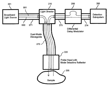
[0057] Fig. 2 shows one example of a sensing device according to one
implementation. This device directs light in two propagation modes
along the same waveguide to an optical probe head near a sample 205 for
acquiring information of optical inhomogeneity in the sample. A sample holder
may be used to support the sample 205 in some applications. Light
radiation from a broadband light source 201 is coupled into the first
dual-mode waveguide 271 to excite two orthogonal propagation modes, 001
and 002. A light director 210 is used to direct the two modes to the
second dual-mode waveguide 272 that is terminated by a probe head 220.
The probe head 220 may be configured to perform at least the following
functions. The first function of the probe head 220 is to reverse the
propagation direction of a portion of light in the waveguide 272 in the
mode 001; the second function of the probe head 220 is to reshape and
deliver the remaining portion of the light in mode 002 to the sample
205; and the third function of the probe head 220 is to collect the
light reflected from the sample 205 back to the second dual-mode
waveguide 272. The back traveling light in both modes 001 and 002 is
then directed by light director 210 to the third waveguide 273 and
further propagates towards differential delay modulator 250. The
differential delay modulator 250 is capable of varying the relative
optical path length and optical-phase between the two modes 001 and 002.
A detection subsystem 260 is used to superpose the two propagation modes
001 and 002 to form two new modes, mutually orthogonal, to be received
by photo-detectors. Each new mode is a mixture of the modes 001 and
002.
[0058] The superposition of the two modes 001 and 002 in the detection
subsystem 260 allows for a range detection. The light entering the
detection subsystem 260 in the mode 002 is reflected by the sample,
bearing information about the optical inhomogeneity of the sample 205,
while the other mode, 001, bypassing the sample 205 inside probe head
220. So long as these two modes 001 and 002 remain independent through
the waveguides their superposition in the detection subsystem 260 may be
used to obtain information about the sample 205 without the separate
optical paths used in some conventional Michelson interferometer
systems.
[0059] For the simplicity of the analysis, consider a thin slice of
the source spectrum by assuming that the amplitude of the mode 001 is
-13-
CA 02528417 2005-12-02
WO 2005/001522 PCT/US2004/017649
E001 in a first linear polarization and that- of the mode 002 is E002 in a
second, orthogonal linear polarization in the first waveguide 271. The
sample 205 can be characterized by an effective reflection coefficient r
that is complex in nature; the differential delay modulator 350 can be
characterized by a pure phase shift r' exerted on the mode 001. Let us
now superpose the two modes 001 and 002 by projecting them onto a pair
of new modes, EA and EB, by a relative 45-degree rotation in the vector
space. The new modes, EA and EB, may be expressed as following:
EA - T
(e/ E001 + rE002 )
(1)
"T
It is assumed that all components in the system, except for the sample
205, are lossless. The resultant intensities of the two superposed modes
are
IA = 2 [E of + Eo02+ r EOOIE002 cos(r - gyp)]
(2)
IB = 2 [E of + E002- r Eoo1E002 cos(r - ()]
where rp is the phase delay associated with the reflection from the
sample. A convenient way to characterize the reflection coefficient r is
to measure the difference of the above two intensities, i.e.
IA - IB =1 r I Eo01E002 cos(r (3)
If r is modulated by the differential delay modulator 250, the measured
signal, Eq. (3), is modulated accordingly. For either a periodic or a
time-linear variation of r, the measured responds with a periodic
oscillation and its peak-to-peak value is proportional to the absolute
value of r.
[0060] For a broadband light source 201 in Fig. 2, consider the two
phases, F and p to be dependent on wavelength. If the two modes 001 and
002 experience significantly different path lengths when they reach the
detection system 260, the overall phase angle, r - (p, should be
significantly wavelength dependant as well. Consequently the measured
signal, being an integration of Eq. (3) over the source spectrum, yields
a smooth function even though F is being varied. The condition for a
significant oscillation to occur in the measured signal is when the two
modes 001 and 002 experience similar path lengths at the location of
-14-
CA 02528417 2005-12-02
WO 2005/001522 PCT/US2004/017649
their superposition. In this case the overall phase angle, r - (p,
becomes wavelength independent or nearly wavelength independent. In
other words, for a given relative path length set by the modulator 250,
an oscillation in the measured signal indicates a reflection, in the
other mode, from a distance that equalizes the optical path lengths
traveled by the two modes 001 and 002. Therefore the system depicted in
Fig. 2 can be utilized for ranging reflection sources.
[0061] Due to the stability of the relative phase between the two
modes, 001 and 002, phase-sensitive measurements can be performed with
the system in Fig. 2 with relative ease. The following describes an
exemplary method based on the system in Fig. 2 for the determination of
the absolute phase associated with the radiation reflected from the
sample 205.
[0062] In this method, a sinusoidal modulation is applied to the
differential phase by the differential delay modulator 250, with a
modulation magnitude of M and a modulation frequency of Q. The
difference in intensity of the two new modes is the measured and can be
expressed as follows:
IA -'B =I r I E001E002 cos[M sin(Qt) - (p] . (4)
It is clear from Eq. (4) that the measured exhibits an oscillation at a
base frequency of S2 and oscillations at harmonic frequencies of the base
frequency fl. The amplitudes of the base frequency and each of the
harmonics are related to q and Irl. The relationships between r and the
harmonics can be derived. For instance, the amplitude of the base-
frequency oscillation and the second harmonic can be found from Eq. (4)
to be:
An=E001E002J1(M) I rI sin (p; (5a)
A2n =E001E002J2(M)I rI cos(p, (5b)
where J1 and J2 are Bessel functions of the first and second order,
respectively. Eq. (5a) and (5b) can be used to solve for Irl and (p, i.e.
the complete characterization of r. We can therefore completely
characterize the complex reflection coefficient r by analyzing the
harmonic content of various orders in the measured signal. In
particular, the presence of the base-frequency component in the measured
is due to the presence of T.
-15-
CA 02528417 2005-12-02
WO 2005/001522 PCT/US2004/017649
[0063] Fig. 3 shows an exemplary implementation of the system depicted
in Fig. 2. The spectrum of source 201 may be chosen to satisfy the
desired ranging resolution. The broader the spectrum is the better the
ranging resolution. Various light sources may be used as the source 201.
For example, some semiconductor superluminescent light emitting diodes
(SLED) and amplified spontaneous emission (ASE) sources may possess the
appropriate spectral properties for the purpose. In this particular
example, a polarization controller 302 may be used to control the state
of polarization in order to proportion the magnitudes of the two modes,
001 and 002, in the input waveguide 371. The waveguide 371 and other
waveguides 372 and 373 may be dual-mode waveguides and are capable of
supporting two independent polarization modes which are mutually
orthogonal. One kind of practical and commercially available waveguide
is the polarization maintaining (PM) optical fiber. A polarization
maintaining fiber can carry two independent polarization modes, namely,
the s-wave polarized along its slow axis and the p-wave polarized along
its fast axis. In good quality polarization maintaining fibers these
two modes can have virtually no energy exchange, or coupling, for
substantial distances. Polarization preserving circulator 310 directs
the flow of optical waves according to the following scheme: the two
incoming polarization modes from fiber 371 are directed into the fiber
372; the two incoming polarization modes from fiber 372 are directed to
the fiber 373. A polarization-preserving circulator 310 may be used to
maintain the separation of the two independent polarization modes. For
instance, the s-wave in the fiber 371 should be directed to the fiber
372 as s-wave or p-wave only. Certain commercially available
polarization-preserving circulators are adequate for the purpose.
[0064] The system in Fig. 3 implements an optical probe head 320
coupled to the waveguide 372 for optically probing the sample 205. The
probe head 320 delivers a portion of light received from the waveguide
372, the light in one mode (e.g., 002) of the two modes 001 and 002, to
the sample 205 and collects reflected and back-scattered light in the
same mode 002 from the sample 205. The returned light in the mode 002
collected from the sample 205 carries information of the sample 205 and
is processed to extract the information of the sample 205. The light in
the other mode 001 in the waveguide 372 propagating towards the probe
head 320 is reflected back by the probe head 320. Both the returned
light in the mode 002 and the reflected light in the mode 001 are
directed back by the probe head 320 into the waveguide 372 and to the
differential delay modulator 250 and the detection system 260 through
the circulator 310 and the waveguide 373.
-16-
CA 02528417 2005-12-02
WO 2005/001522 PCT/US2004/017649
[0065] In the illustrated implementation, the probe head 320 includes
a lens system 321 and a polarization-selective reflector (PSR) 322. The
lens system 321 is to concentrate the light energy into a small area,
facilitating spatially resolved studies of the sample in a lateral
direction. The polarization-selective reflector 322 reflects the mode
001 back and transmits the mode 002. Hence, the light in the mode 002
transmits through the probe head 320 to impinge on the sample 205. Back
reflected or scattered the light from the sample 205 is collected by the
lens system 321 to propagate towards the circulator 310 along with the
light in the mode 001 reflected by PSR 322 in the waveguide 372.
[0066] Fig. 4 shows details of the probe head 320 and an example of
the polarization-selective reflector (PSR) 322 according to one
implementation. The PSR 322 includes a polarizing beam splitter (PBS)
423 and a reflector or mirror 424 in a configuration as illustrated
where the PBS 423 transmits the selected mode (e.g., mode 002) to the
sample 205 and reflects and diverts the other mode (e.g., mode 001) away
from the sample 205 and to the reflector 424. By retro reflection of
the reflector 424, the reflected mode 001 is directed back to the PBS
423 and the lens system 321. The reflector 424 may be a reflective
coating on one side of beam splitter 423. The reflector 424 should be
aligned to allow the reflected radiation to re-enter the polarization-
maintaining fiber 372. The transmitted light in the mode 002 impinges
the sample 205 and the light reflected and back scattered by the sample
205 in the mode 002 transmits through the PBS 423 to the lens system
321. The lens system 321 couples the light in both the modes 001 and
002 into the fiber 372.
[0067] In the implementation illustrated in Fig. 3, the detection
system 260 includes a polarizing beam splitter 361, and two
photodetectors 362 and 363. The polarizing beam splitter 361 is used to
receive the two independent polarization modes 001 and 002 from the
modulator 250 and superposes the two independent polarization modes 001
and 002. The beam splitter 361 may be oriented in such a way that, each
independent polarization is split into two parts and, for each
independent polarization mode, the two split portions possess the same
amplitude. This way, a portion of the mode 001 and a portion of the
mode 002 are combined and mixed in each of the two output ports of the
beam splitter 361 to form a superposed new mode and each photodetector
receives a superposed mode characterized by Eq. (1). The polarizing
beam splitter 361 may be oriented so that the incident plane of its
reflection surface makes a 45-degree angle with one of the two
independent polarization mode, 001 or 002.
-17-
CA 02528417 2005-12-02
WO 2005/001522 PCT/US2004/017649
[0068] The system in Fig. 3 further implements an electronic
controller or control electronics 370 to receive and process the
detector outputs from the photodetectors 362 and 363 and to control
operations of the systems. The electronic controller 370, for example,
may be used to control the probe head 320 and the differential delay
modulator 25,0. Differential delay modulator 250, under the control of
the electronics and programs, generates a form of differential phase
modulation as the differential path length scans through a range that
matches a range of depth inside the sample 205. The electronic
controller 370 may also be programmed to record and extract the
amplitude of the oscillation in the measured signal characterized by Eq.
(3) at various differential path lengths generated by the modulator 250.
Accordingly, a profile of reflection as a function of the depth can be
obtained as a one-dimensional representation of the sample inhomogeneity
at a selected location on the sample 205.
[0069] For acquiring two-dimensional images of optical inhomogeneity
in the sample 205, the probe head 320 may be controlled via a position
scanner such as a translation stage or a piezo-electric positioner so
that the probing light scans in a lateral direction, perpendicular to
the light propagation direction. For every increment of the lateral scan
a profile of reflection as a function of depth can be recorded with the
method described above. The collected information can then be displayed
on a display and interface module 372 to form a cross-sectional image
that reveals the inhomogeneity of the sample 205.
[0070] In general, a lateral scanning mechanism may be implemented in
each device described in this application to change the relative lateral
position of the optical probe head and the sample to obtain a 2-
dimensional map of the sample. A xy-scanner, for example, may be
engaged either to the optical head or to a sample holder that holds the
sample to effectuate this scanning in response to a position control
signal generated from the electronic controller 370.
[0071] FIGS. 5A and 5B illustrate another exemplary system that use
waveguides 271, 272, and 273 and a light director 210 to direct light in
two modes to and from the probe head 320 in measuring the sample 205. A
first optical polarizer 510 is oriented with respect to the polarization
axes of the PM waveguide 271 to couple radiation from the broadband
light source 201 into the waveguide 271 in two orthogonal linear
polarization modes as the independent propagation modes. An optical
phase modulator 520 is coupled in the waveguide 271 to modulate the
optical phase of light in one guided mode relative to the other. A
variable differential group delay (VDGD) device 530 is inserted in or
~18-
CA 02528417 2005-12-02
WO 2005/001522 PCT/US2004/017649
connected to the waveguide 273 to introduce a controllable amount of
optical path difference between the two waves. A second optical
polarizer 540 and an optical detector 550 are used here to form a
detection system. The second polarizer 540 is oriented to project both
of the guided waves onto the same polarization direction so that the
changes in optical path difference and the optical phase difference
between the two propagation modes cause intensity variations, detectable
by the detector 550.
[0072] The light from the source 201 is typically partially polarized.
The polarizer 510 may be aligned so that maximum amount of light from
the source 201 is transmitted and that the transmitted light is coupled
to both of the guided modes in the waveguide 271 with the substantially
equal amplitudes. The electric fields for the two orthogonal
polarization modes S and P in the waveguide 271 can be expressed as:
ES = E,
(6)
Ep= E.
where the electric field transmitting the polarizer is denoted as E. It should
be
appreciated that the light has a finite spectral width (broadband or partially
coherent). The fields can be described by the following Fourier integral:
E = f EG,e'-"dcv . (7)
For the simplicity of the analysis, a thin slice of the spectrum, i.e. a
lightwave
of a specific wavelength, is considered below. Without loosing generality, it
is
assumed that all the components, including polarizers, waveguides, Router, PSR
and
VDGD, are lossless. Let us designate the reflection coefficient of the sample
r,
that is complex in nature. The p-wave picks up an optical phase, IT, relative
to the
s-wave as they reach the second polarizer 540:
E,=
12- E,
(8)
Ep = rEe'T.
The light that passes through Polarizer 540 can be expressed by
-19-
CA 02528417 2005-12-02
WO 2005/001522 PCT/US2004/017649
Ea=-(E5+Ep)=2E(1+re'T). (9)
The intensity of the light that impinges on the photodetector 550 is given by:
I =E,,Ea = JEI2[1+Ir!2+21rlcos(r+8)]. (10)
where phase angle S reflects the complex nature of the reflection coefficient
of the
sample 205 and is defined by
r=lrle''. (11)
Assuming the modulator 520 exerts a sinusoidal phase modulation, with
magnitude M
and frequency 0, in the p-wave with respect to the s-wave, the light intensity
received by the detector 550 can be expressed as follows:
I = 1 + 4 rl I I2 + I~ 2 I I I2 cos[M sin(Qt) + +'5] . (12)
where phase angle V is the accumulated phase slip between the two modes, not
including the periodic modulation due to the modulator 520. The VDGD 530 or a
static phase shift in the modulator 520, may be used to adjust the phase
difference
between the two modes to eliminate (p.
The waveform of I is graphically shown in Fig. 4.
[0073] FIG. 6 illustrates the waveform of the intensity I received at
the detector 550 as a function of the phase. The detected light
intensity exhibits an oscillating waveform that possesses a base
frequency of .(2 and its harmonics. The amplitudes of the base frequency
and each of the harmonics are related to S and Iri. The mathematical
expressions for the relationships between r and the harmonics can be
derived. For instance, the amplitude of the base-frequency oscillation
and the second harmonic are found to be:
-20-
CA 02528417 2005-12-02
WO 2005/001522 PCT/US2004/017649
Ac = 0.5IEI2J,(M)Irlsin8 ; (13a)
-420= 0.5 IEI2 J2 (M)Irl cos 15, (13b)
where J1 and J2 are Bessel functions of the first and second order,
respectively. Eq. (13a) and (13b) can be used to solve for Iri and
i.e. the complete characterization of r.
[0074] The effect of having a broadband light source 201 in the system
in FIGS. 5A and 5B is analyzed below. When there is a significant
differential group delay between the two propagation modes there must be
an associated large phase slippage (p that is wavelength dependent. A
substantial wavelength spread in the light source means that the phase
slippage also possesses a substantial spread. Such a phase spread cannot
be eliminated by a phase control device that does not also eliminate the
differential group delay. In this case the detected light intensity is
given by the following integral:
1 2
rl IE(A)I2 + I2 IE(2)I2 cos[M sin(Qt) + P(2) + 8] d2 . (14)
J r 1 + I 4 2
It is easy to see that if the range of cp(2) is comparable to it for the
bandwidth of the light source no oscillation in I can be observed as
oscillations for different wavelengths cancel out because of their phase
difference. This phenomenon is in close analogy to the interference of
white light wherein color fringes are visible only when the path
difference is small (the film is thin). The above analysis demonstrates
that the use of a broadband light source enables range detection using
the proposed apparatus. In order to do so, let the s-wave to have a
longer optical path in the system compared to the p-wave (not including
its round-trip between Probing Head and Sample). For any given path
length difference in the system there is a matching distance between
Probing Head and Sample, z, that cancels out the path length difference.
If an oscillation in I is observed the p-wave must be reflected from this
specific distance z. By varying the path length difference in the system
and record the oscillation waveforms we can therefore acquire the
reflection coefficient r as a function of the longitudinal distance z,
-21-
CA 02528417 2005-12-02
WO 2005/001522 PCT/US2004/017649
or depth. By moving Probing Head laterally, we can also record the
variation of r in the lateral directions.
[0075] FIG. 7 further shows one exemplary operation of the described system in
FIG. 5B or the system in FIG. 3 for acquiring images of optical inhomogeneity.
At
step 710, the relative phase delay between the two modes is changed, e.g.,
increased
by an increment, to a fixed value for measuring the sample 205 at a
corresponding
depth. This may be accomplished in FIG. 5B by using the differential delay
device
530 or the bias in the differential delay modulator 250 in FIG. 3. At step
720, a
modulation driving signal is sent to the modulator 520 in FIG. 5B or the
modulator
250 in FIG. 3 to modulate the relative phase delay between the two modes
around the
fixed value. At step 730, the intensity waveform received in the detector 550
in
FIG. 5B or the intensity waveforms received in the detectors 362,363 in FIG. 3
are
measured and stored in the electronic controller 370. Upon completion of the
step
730, the electronic controller 370 controls the differential delay device 530
in
FIG. 5B or the bias in the differential delay modulator 250 in FIG. 3 to
change the
relative phase delay between the two modes to a different fixed value for
measuring
the sample 205 at a different depth. This process iterates as indicated by the
processing loop 740 until desired measurements of the sample at different
depths at
the same location are completed. At this point, electronic controller 370
controls
the probe head 320 to laterally move to a new location on the sample 205 and
repeat
the above measurements again until all desired locations on the sample 205 are
completed. This operation is represented by the processing loop 750. The
electronic controller 370 processes each measurement to compute the values of
S and
Irl from the base oscillation and the harmonics at step 760. Such data
processing may be performed after each measurement or after all
measurements are completed. At step 770, the computed data is sent to
the display module 372.
[0076] In the above implementations, light for sensing the sample 205
is not separated into two parts that travel along two different optical
paths. Two independent propagation modes of the light are guided
essentially in the same waveguide at every location along the optical
path except for the extra distance traveled by one mode between the
probe head 320 and the sample 205. After redirected by the probe head
320, the two modes are continuously guided in the same waveguide at
every location along the optical path to the detection module.
[0077] Alternatively, the light from the light source to the probe
head may be controlled in a single propagation mode (e.g., a first
propagation mode) rather than two different modes. The probe head may
be designed to cause a first portion of the first mode to reverse its
propagation direction while directing the remaining portion, or a second
portion, to reach the sample. The reflection or back scattered light of
-22-
CA 02528417 2005-12-02
WO 2005/001522 PCT/US2004/017649
the second portion from the sample is collected by the probe head and is
controlled in the second propagation mode different from the first mode
to produce a reflected second portion. Both the reflected first portion
in the first propagation mode and the reflected second portion in the
second propagation mode are directed by the probe head through a common
waveguide into the detection module for processing. In comparison with
the implementations that use light in two modes throughout the system,
this alternative design further improves the stability of the relative
phase delay between the two modes at the detection module and provides
additional implementation benefits.
[0078] FIGS. 8A and 8B illustrate one exemplary design of the optical
layout of the optical sensing system and its system implementation with
an electronic controller. An input waveguide 871 is provided to direct
light in a first propagation mode, e.g., the mode 001, from the
broadband light source 201 to a light director 810. The waveguide 871
may be a mode maintaining waveguide designed to support at least one
propagation mode such as the mode 001 or 002. When light is coupled
into the waveguide 871 in a particular mode such as the mode 001, the
waveguide 871 essentially maintains the light in the mode 001. A
polarization maintaining fiber supporting two orthogonal linear
polarization modes, for example, may be used as the waveguide 871.
Similar to systems shown in FIGS. 2, 3, 5A and 5B, dual-mode waveguides
272 and 273 are used to direct the light. A light director 510 is used
to couple the waveguides 871, 272, and 273, to convey the mode 001 from
the input waveguide 871 to one of the two modes (e.g., modes 001 and
002) supported by the dual-mode waveguide 272, and to direct light in
two modes from the waveguide 272 to the dual-mode waveguide 273. In the
example illustrated in FIG. 8A, the light director 810 couples the light
in the mode 001 from the waveguide 871 into the same mode 001 in the
waveguide 272. Alternatively, the light director 810 may couple the
light in the mode 001 from the waveguide 871 into the different mode 002
in the waveguide 272. The dual-mode waveguide 271 is terminated at the
other end by a probe head 820 which couples a portion of light to the
sample 205 for sensing.
[0079] The probe head 820 is designed differently from the prove head
320 in that the probe head 830 converts part of light in the mode 001
into the other different mode 002 when the light is reflected or
scattered back from the sample 205. Alternatively, if the light in the
waveguide 272 that is coupled from the waveguide 871 is in the mode 002,
the probe head 820 converts that part of light in the mode 002 into the
other different mode 001 when the light is reflected or scattered back
-23-
CA 02528417 2005-12-02
WO 2005/001522 PCT/US2004/017649
from the sample 205. In the illustrated example, the probe head 820
performs these functions: a) to reverse the propagation direction of a
small portion of the incoming radiation in mode 001; b) to reshape the
remaining radiation and transmit it to the sample 205; and c) to convert
the radiation reflected from the sample 205 to an independent mode 002
supported by the dual-mode waveguide 272. Since the probe head 820 only
converts part of the light into the other mode supported by the
waveguide 272, the probe head 820 is a partial mode converter in this
regard. Due to the operations of the probe head 820, there are two
modes propagating away from the probe head 820, the mode 001 that
bypasses the sample 205 and the mode 002 for light that originates from
sample reflection or back scattering. From this point on, the structure
and operations of the rest of the system shown in FIG. 8A may be similar
to the systems in FIGS. 2, 3, 5A, and 5B.
[0080] FIG. 8B shows an exemplary implementation of the design in FIG.
8A where an electronic controller 3370 is used to control the
differential delay modulator 250 and the probe head 820 and a display
and interface module 372 is provided. Radiation from broadband light
source 201, which may be partially polarized, is further polarized and
controlled by an input polarization controller 802 so that only a single
polarization mode is excited in polarization-maintaining fiber 371 as
the waveguide 871 in FIG. 8A. a polarization preserving circulator may
be used to implement the light director 810 for routing light from the
waveguide 371 to the waveguide 372 and from the waveguide 372 to the
waveguide 373.
[0081] The probe head 820 in FIG. 8B may be designed to include a lens
system 821 similar to the lens system 321, a partial reflector 822, and
a polarization rotator 823. The partial reflector 822 is used to
reflect the first portion of light received from the waveguide 372 back
to the waveguide 372 without changing its propagation mode and transmits
light to and from the sample 205. The polarization rotator 823 is used
to control the light from the sample 205 to be in the mode 002 upon
entry of the waveguide 372.
[0082] FIG. 9 shows another example of a system implementation where
the optical probe head 820 receives light in a single input mode and
converts part of light into a different mode. An input polarizer 510 is
used in the input PM fiber 272 to control the input light in the single
polarization mode. A phase modulator 520 and a variable differential
group delay device 530 are coupled to the output PM fiver 273 to control
and modulate the relative phase delay of the two modes before optical
detection. An output polarizer 540 is provided to mix the two modes and
-24-
CA 02528417 2005-12-02
WO 2005/001522 PCT/US2004/017649
the detector 550 is used to detect the output from the output polarizer
540.
[0083] FIGS. 10A and 10B show two examples of the possible designs for
the probe head 820 including a partially reflective surface 1010, a lens
system 1020, and a quarter-wave plate 1030 for rotating the polarization
and to convert the mode. In FIG. 10A, the termination or end facet of
polarization-maintaining fiber 372 is used as the partial reflector
1010. An uncoated termination of an optical fiber reflects
approximately 4% of the light energy. Coatings can be used to alter the
reflectivity of the termination to a desirable value. The lens system
1020 reshapes and delivers the remaining radiation to sample 205. The
other role played by the lens system 1020 is to collect the radiation
reflected from the sample 205 back into the polarization-maintaining
fiber 372. The quarter wave plate 1030 is oriented so that its optical
axis make a 45-degree angle with the polarization direction of the
transmitted light. Reflected light from the sample 205 propagates
through the quarter wave plate 1030 once again to become polarized in a
direction perpendicular to mode 001, i.e. mode 002. Alternatively, the
quarter wave plate 1030 may be replaced by a Faraday rotator. The head
design in FIG. 10B changes the positions of the lens system 1020 and the
quarter wave plate or Faraday rotator 1030.
[0084] In the examples in FIGS. 8A, 8B, and 9, there is only one
polarization mode entering the light director 810 or the polarization-
preserving circulator from waveguide 871 or 371. Therefore, the light
director 810 or the polarization preserving circulator may be
constructed with a polarization-maintaining optical circulator 1110 and
two polarization beam splitters 1120 and 1130 as shown in FIG. 11. The
polarization-maintaining circulator 1110 is used to convey only one
polarization mode among its three ports, rather than both modes as in
the case shown in FIGS. 3, 5A and 5B. The polarizing beam splitter 1120
and 1130 are coupled to polarization-maintaining circulator 1110 so that
both polarization modes entering Port 2 are conveyed to Port 3 and
remain independent.
[0085] A number of hardware choices are available for differential
delay modulator 250. FIG. 12 illustrates the general design of the
modulator 250 where an external control signal is applied to control a
differential delay element to change and modulate the relative delay in
the output. Either mechanical or non-mechanical elements may be used to
produce the desired relative delay between the two modes and the
modulation on the delay.
-25-
CA 02528417 2005-12-02
WO 2005/001522 PCT/US2004/017649
[0086] In one implementation, a non-mechanical design may include one
or more segments of tunable birefringent materials such as liquid
crystal materials or electro-optic birefringent materials such as
lithium niobate crystals in conjunction with one or more fixed
birefringent materials such as quartz and rutile. The fixed
birefringent material provides a fixed delay between two modes and the
tunable birefringent material provides the tuning and modulation
functions in the relative delay between the two modes. FIG. 12A
illustrates an example of this non-mechanical design where the two modes
are not physically separated and are directed through the same optical
path with birefringent segments which alter the relative delay between
two polarization modes.
[0087] FIG. 12B shows a different design where the two modes in the
received light are separated by a mode splitter into two different
optical paths. A variable delay element is inserted in one optical path
to adjust and modulate the relative delay in response to an external
control signal. A mode combiner is then used to combine the two modes
together in the output. The mode splitter and the mode combiner may be
polarization beams splitters when two orthogonal linear polarizations
are used as the two modes.
[0088] The variable delay element in one of the two optical paths may
be implemented in various configurations. For example, the variable
delay element may be a mechanical element. A mechanical implementation
of the device in FIG. 12B may be constructed by first separating the
radiation by polarization modes with a polarizing beam splitter, one
polarization mode propagating through a fixed optical path while the
other propagating through a variable optical path having a piezoelectric
stretcher of polarization maintaining fibers, or a pair of collimators
both facing a mechanically movable retroreflector in such a way that the
light from one collimator is collected by the other through a trip to
and from the retroreflector, or a pair collimators optically linked
through double passing a rotatable optical plate and bouncing off a
reflector.
[0089] FIGS. 13A and 13B illustrate two examples of a mechanical
variable delay element suitable for FIG. 12B. Such a mechanical
variable delay device may be used to change the optical path length of a
light beam at high speeds and may have various applications other than
what is illustrated in FIG. 12B. In addition, the optical systems in
this application may use such a delay device.
[0090] The mechanical delay device shown in FIG. 13A includes an
optical beam splitter 1310, a rotating optical plate 1320 which may be a
-26-
CA 02528417 2005-12-02
WO 2005/001522 PCT/US2004/017649
transparent plate, and a mirror or reflector 1330. The beam splitter
1310 is used as the input port and the output port for the device. The
rotating optical plate 1320 is placed between the mirror 1330 and the
beam splitter 1310. The input light beam 1300 is received by the beam
splitter 1310 along the optical path directing from the beam splitter
1310 to the mirror 1330 through the rotating optical plate 1320. A
portion of the light 1300 transmitting through the beam splitter 1310 is
the beam 1301 which impinges on and transmits through the rotating
optical plate 1320. The mirror or other optical reflector 1330 is
oriented to be perpendicular to the light beam incident to the optical
plate 1310 from the opposite side. The reflected light beam 1302 from
the mirror 1320 traces the same optical path back traveling until it
encounters the Beam Splitter 1310. The Beam Splitter 1310 deflects part
of the back traveling light 1302 to a different direction as the output
beam 1303.
[0091] In this device, the variation of the optical path length is
caused by the rotation of the Optical Plate 1320. The Optical Plate 1320
may be made of a good quality optical material. The two optical surfaces
may be flat and well polished to minimize distortion to the light beam.
In addition, the two surfaces should be parallel to each other so that
the light propagation directions on both sides of the Optical Plate 1320
are parallel. The thickness of the Optical Plate 1320 may be chosen
according to the desirable delay variation and the range of the rotation
angle. The optical path length experienced by the light beam is
determined by the rotation angle of the Optical Plate 1320. When the
surfaces of the Optical Plate 1320 is perpendicular to the light beam
(incident angle is zero), the path length is at its minimum. The path
length increases as the incident angle increases.
[0092] In FIG. 13A, it may be beneficial to collimate the input light
beam so that it can travel the entire optical path without significant
divergence. The Optical Plate 1320 may be mounted on a motor for
periodic variation of the optical delay. A good quality mirror with a
flat reflecting surface should be used to implement the mirror 1330. The
reflecting surface of the mirror 1330 may be maintained to be
perpendicular to the light beam.
[0093] If a linearly polarized light is used as the input beam 1300 in
FIG. 13A, it is beneficial to have the polarization direction of the
light parallel to the incident plane (in the plane of the paper) as less
reflection occurs at the surfaces of Optical Plate 1320 for this
polarization compared to other polarization directions. Antireflection
-27-
CA 02528417 2005-12-02
WO 2005/001522 PCT/US2004/017649
coatings can be used to further reduce the light reflection on the
surfaces of the Optical Plate 1320.
[0094] The beam splitter 1310 used in Fig. 13A uses both its optical
transmission and optical reflection to direct light. This aspect of the
beam splitter 1310 causes reflection loss in the output of the device
due to the reflection loss when the input light 1300 first enters the
device through transmission of the beam splitter 1310 and the
transmission loss when the light exits the device through reflection of
the beam splitter 1310. For example, a maximum of 25% of the total
input light may be left in the output light if the beam splitter is a
50/50 beam splitter. To avoid such optical loss, an optical circulator
may be used in place of the beam splitter 1320. FIG. 13B illustrates an
example where the optical circulator 1340 with 3 ports is used to direct
input light to the optical plate 1320 and the mirror 1330 and directs
returned light to the output port. The optical circulator 1340 may be
designed to direct nearly all light entering its port 1 to port 2 and
nearly all light entering its port 2 to the port 3 with nominal optical
loss and hence significantly reduces the optical loss in the device.
Commercially available optical circulators, either free-space or fiber-
based, may be used to implement the circulator 1340.
[0095] FIG. 14A shows an exemplary implementation of the delay device
in FIG. 12B as part of or the entire differential delay modulator 250.
A first optical mode splitter 1410 is used to separate two modes in the
waveguide 373 into two paths having two mirrors 1431 and 1432,
respectively. A second optical mode splitter 1440, which is operated as
a mode combiner, is used to combine the two modes into an output. If
the two modes are two orthogonal linear polarizations, for example,
polarization beam splatters may be used to implement the 1410 and 1440.
A variable optical delay line or device 1420 is placed in the upper path
to control the differential delay between the two paths. The output may
be coupled into another dual-mode waveguide 1450 leading to the
detection module or directly sent into the detection module. FIG. 14B
shows a delay device based on the design in FIG. 14A where the mirror
1432 and the variable optical delay line 1420 are implemented by the
mechanical delay device in FIG. 13A. The mechanical delay device in
FIG. 13B may also be used to implement the device in FIG. 14A.
[0096] In the above examples, a single dual-mode waveguide 272 or 372
is used as an input and output waveguide for the probe head 220, 320, or
820. Hence, the input light, either in a single mode or two independent
modes, is directed into the probe head through that dual-mode waveguide
-28-
CA 02528417 2005-12-02
WO 2005/001522 PCT/US2004/017649
272 or 372, and the output light in the two independent modes is also
directed from the probe head to the detection subsystem or detector.
[0097] Alternatively, the single dual-mode waveguide 272 or 372 may be
replaced by two separate waveguides, one to direct input light from the
light source to the probe head and another to direct light from the
probe head to the detection subsystem or detector. As an example, the
device in FIG. 2 may have a second waveguide different from the
waveguide 272 to direct reflected light in two different modes from the
optical probe head 220 to the modulator 250 and the detection subsystem
260. In this design, the light director 210 may be eliminated. This
may be an advantage. In implementation, the optics within the probe
head may be designed to direct the reflected light in two modes to the
second waveguide.
[0098] FIG. 15 illustrates an example for this design as an
alternative to the device shown in FIG. 5B. In this design, the probing
light is delivered to the sample 205 through one dual-mode waveguide
1510 and the reflected/scattered light is collected by the probe head
320 and is directed through another dual-mode waveguide 1520. With the
probe head shown in FIG. 4, the mirror 424 may be oriented and aligned
so that the light is reflected into the waveguide 1520 instead of the
waveguide 1510. This design may be applied to other devices based on the
disclosure of this application, including the exemplary devices in FIGS.
2, 3, 8A, 8B and 9.
[0099] The above-described devices and techniques may be used to
obtain optical measurements of a given location of the sample at
different depths by controlling the relative phase delay between two
modes at different values and optical measurements of different
locations of the sample to get a tomographic map of the sample at a
given depth or various depths by laterally changing the relative
position of the probe head over the sample. Such devices and techniques
may be further used to perform other measurements on a sample, including
spectral selective measurements on a layer of a sample.
[00100] In various applications, it may be beneficial to obtain
information about certain substances, identifiable through their
spectral absorbance, dispersed in the samples. For this purpose, a
tunable bandpass filter may be used to either filter the light incident
to the probe head to select a desired spectral window within the
broadband spectrum of the incident light to measure the response of the
sample and to vary the center wavelength of the spectral window to
measure a spectral distribution of the responses of the sample. This
tuning of the bandpass filter allows a variable portion of the source
-29-
CA 02528417 2005-12-02
WO 2005/001522 PCT/US2004/017649
spectrum to pass while measuring the distribution of the complex
reflection coefficient of the sample.
[00101] Alternatively, the broadband light may be sent to the optical
probe head without optical filtering and the spectral components at
different wavelengths in the output light from the probe head may be
selected and measured to measure the response of the sample around a
selected wavelength or the spectral distribution of the responses of the
sample. In one implementation, a tunable optical bandpass filter may be
inserted in the optical path of the output light from the probe head to
filter the light. In another implementation, a grating or other
diffractive optical element may be used to optically separate different
spectral components in the output light to be measured by the detection
subsystem or the detector.
[00102] As an example, FIG. 16 shows a system based on the design in
FIG. 2 where a tunable filter 1610 is inserted in the input waveguide
271 to filter the input light in two different modes. FIG. 17 shows
another exemplary system based on the design in FIG. 8A where a tunable
filter 1710 is inserted in the input waveguide 871 to filter the input
light in a single mode. Such a tunable filter may be placed in other
locations.
[00103] FIG. 18 illustrates the operation of the tunable bandpass
filter in the devices in FIGS. 16 and 17. The filter selects a narrow
spectral band within the spectrum of the light source to measure the
spectral feature of the sample.
[00104] Notably, the devices and techniques of this application may be
used to select a layer within a sample to measure by properly processing
the measured data. Referring back to the devices in FIGS. 16 and 17,
let us assume that the absorption characteristics of a layer bounded by
interfaces I and II is to be measured. For the simplicity of
description, it is assumed that the spectral absorption of the substance
in the layer is characterized by a wavelength-dependent attenuation
coefficient ph (A.) and that of other volume is characterized by ft9(i%) . It
is further assumed that the substance in the vicinity of interface I
(II) possesses an effective and wavelength independent reflection
coefficient r2 (r11). If the characteristic absorption of interest is
covered by the spectrum of the light source, an optical filter 1610 or
1710 with a bass band tunable across the characteristic absorption of
the sample 205 may be used to measure the spectral responses of the
sample 205 centered at different wavelengths.
[00105] In operation, the following steps may be performed. First, the
differential delay modulator 250 is adjusted so that the path length
-30-
CA 02528417 2005-12-02
WO 2005/001522 PCT/US2004/017649
traveled by one mode (e.g., the mode 001) matches that of radiation
reflected from interface I in the other mode (e.g., the mode 002). At
this point, the pass band of filter 1610 or 1710 may be scanned while
recording the oscillation of the measured signal due to a periodic
differential phase generated by the modulator 250. The oscillation
amplitude as a function of wavelength is given by
AI( )-rIe-2,ug(A)Z`
(15)
where zr is the distance of interface I measured from the top surface of
the sample 205. Next, the differential delay modulator 250 is adjusted
again to change the differential delay so that the path length traveled
by the mode 001 matches that of radiation reflected from interface II in
the mode 002. The measurement for the interface II is obtained as
follows:
A Y e -2,,,, ( 2)Z, -2,U1, (A)zu (16 )
II(A) = II
where z11 is the distance of interface II measured from interface I. To
acquire the absorption characteristics of the layer bounded by the
interfaces I and II, Eq. (7) and Eq. (6) can be used to obtain the
following ratio:
All (A) _ rII e tun (2)ZU (17)
AI (A,) '"I
Notably, this equation provides the information on the absorption
characteristics of the layer of interest only and this allows
measurement on the layer. This method thus provides a "coherence
gating" mechanism to optically acquire the absorbance spectrum of a
particular and designated layer beneath a sample surface.
[00106] It should be noted that the pass band of the optical filter
1610 or 1710 may be designed to be sufficiently narrow to resolve the
absorption characteristics of interest and at the meantime broad enough
to differentiate the layer of interest. The following example for
monitoring the glucose level by optically probing a patient's skin shows
that this arrangement is reasonable and practical.
[00107] Various dependable glucose monitors rely on taking blood
samples from diabetes patients. Repeated pricking of skin can cause
considerable discomfort to patients. It is therefore desirable to
-31"-
CA 02528417 2005-12-02
WO 2005/001522 PCT/US2004/017649
monitor the glucose level in a noninvasive manner. It is well known
that glucose in blood possesses "signature" optical absorption peaks in
a near-infrared (NIR) wavelength range. It is also appreciated the main
obstacle in noninvasive monitoring of glucose is due to the fact that a
probing light beam interacts, in its path, with various types of tissues
and substances which possess overlapping absorption bands. Extracting
the signature glucose peaks amongst all other peaks has proven
difficult.
[00108] The above "coherence gating" may be used overcome the
difficulty in other methods for monitoring glucose. For glucose
monitoring, the designated layer may be the dermis layer where glucose
is concentrated in a network of blood vessels and interstitial fluid.
[00109] FIG. 19A illustrates an example of a human skin tissue where
the coherence gating technique described here can be used to measure the
glucose concentration in the dermis layer between the epidermis and the
subcutaneous layers. The dermis layer may be optically selected and
measured with the coherence gating technique. It is known that the
superficial epidermis layer, owing to its pigment content, is the
dominant source of NIR absorption. Because of the absence of blood,
however, the epidermis yields no useful information for glucose
monitoring. The coherent gating technique can be applied to acquire
solely the absorbance spectrum of the dermis layer by rejecting the
absorptions of the epidermis and the subcutaneous tissues. An additional
advantage of this technique is from the fact that dermis exhibits less
temperature variation compared to the epidermis. It is known that
surface temperature variation causes shifts of water absorption,
hampering glucose monitoring.
[00110] FIG. 19B shows some predominant glucose absorption peaks in
blood in a wavelength range between 1 and 2.5 microns. The width of
these peaks are approximately 150 nm. To resolve the peaks, the
bandwidth of the tunable bandpass filter may be chosen to be around 30
nm. The depth resolution is determined by the following equation:
21n(2) ~02 = 60,um (18 )
Therefore, the coherence gating implemented with the devices in FIGS. 16
and 17 or other optical sensing devices may be used to determine the
absorption characteristics of the glucose in tissue layers no less than
60 gm thick. As illustrated in FIG. 19A, human skin consists of a
superficial epidermis layer that is typically 0.1 mm thick. Underneath
-32-
CA 02528417 2005-12-02
WO 2005/001522 PCT/US2004/017649
epidermis is the dermis, approximately 1 mm thick, where glucose
concentrates in blood and interstitial fluids. The above analysis
indicates that it is possible to use the apparatus shown in FIGS. 16 and
17 to isolate the absorption characteristics of the dermis from that of
the epidermis and other layers.
[00111] It is clear from Eq. (18) that the product of spectral
resolution and layer resolution is a constant for a given center
wavelength ko. The choice of the filter bandwidth should be made based on
the tradeoff between these two resolutions against the specific
requirements of the measurement.
[00112] The tunable bandpass filter 1610 or 1710 may be operated to
acquire the absorption characteristics of an isolated volume inside a
sample.
[00113] FIG. 20 illustrates one exemplary implementation of the
detection subsystem 260 in FIG. 3 where two diffraction gratings 2010
and 2020 are used to separate different spectral components in the
output light beams from the polarizing beam splitter 361. A lens 2012
is positioned to collect the diffracted components from the grating 2010
and focus different spectral components to different locations on its
focal plane. A detector array 2014 with multiple photodetector elements
is placed at the focal plane of the lens 2012 so that different spectral
components are received by different photodetector elements. A second
lens 2022 and a detector array 2024 are used in the optical path of the
diffracted components in a similar way. In devices shown in FIGS. 5A,
5B, 8A, and 8B where a single optical detector is used for measurements,
a single grating, a lens, and a detector array may be used.
[00114] In operation, each detector element receives light in a small
wavelength interval. The photocurrents from all elements in an array
can be summed to form a signal which is equivalent to the signal
received in each single detector without the grating shown in FIG. 3. By
selectively measuring the photocurrent from an individual element or a
group of elements in an array, the spectral information of the sample
can be obtained.
[00115] In the above described examples, the optical probe head sends
out light in two different propagation modes where light in one of the
two modes carries the information from the sample. Alternatively, light
in a single propagation mode may be used as the input light to the
optical probe head and as output light from the optical probe head.
Hence, devices based on this design not only use a common optical path
to direct light to and from the probe head and sample but also control
the light in a single mode. In comparison with above examples where two
-33-
CA 02528417 2005-12-02
WO 2005/001522 PCT/US2004/017649
different modes are used for light coming out of the probe heads, this
single-mode design further eliminates or reduces any differences between
different modes that propagate in the same optical path.
[00116] FIG. 21 shows one exemplary system for acquiring information of
optical
inhomogeneity and other properties in substances with only one propagation
mode
inside waveguides. A broadband or low-coherence light from Broadband Light
Source 201 is directed to a probe head 2110 by means of polarization-
maintaining waveguides 271 and 272. A partial reflector inside the
probe head 2110 reverses the direction of a small portion of the input
light to create a radiation wave 1 while transmitting the remainder of
the input light to the sample 205. Backscattered or reflected light
from the sample 205 becomes a second radiation wave 2 and is collected
by the probe head 2110. The probe head 2110 combines and couples both
the radiation waves 1 and 2 back into the waveguide 272. The radiation
waves 1 and 2 travel in the waveguide 272 towards Light the light
director 210 which directs radiation waves 1 and 2 through the waveguide
273 towards the detection module 2101. Notably, the radiation waves 1
and 2 output from the probe head 2110 are in the same mode as the input
light to the probe head 2110. the probe head 2110 does not change the
mode of light when directing the radiation waves 1 and 2 to the
waveguide 272.
[00117] The detection module 2101 includes a beam Splitter 2120, two
optical paths 2121 and 2122, an optical variable delay element 2123 in
the path 2122, a beam combiner 2130, and two optical detectors 2141 and
2142. The beam splitter 2120 splits the light in the waveguide 273,
which includes the radiation waves 1 and 2 in the same mode, into two
parts that respectively propagate in the two optical paths 2121 and
2122. Notably, each of the two parts includes light from both the
radiation waves 1 and 2. The variable delay element or delay line 2123
in the optical path 2122 is controlled by a control signal to adjust the
relative optical delay between the two optical paths 2121 and 2122 and
may be implemented by, e.g., the exemplary delay elements described in
this application and other delay designs. The beam combiner 2130
combines the signals of the two optical paths to overlap with each other
and to output two optical signals for optical detectors 2141 and 2142,
respectively. The beam combiner may be a polarization beam splitter
which splits the combined light into two parts, orthogonal in
polarization to one another.
[00118] The probe head 2110 may include a partial reflector to produce
the radiation wave 1 which does not reach the sample 205. Assuming the
single propagation mode for the light to the probe head 2110 and the
-34-
CA 02528417 2005-12-02
WO 2005/001522 PCT/US2004/017649
light out of the probe head 21110 is a polarization mode, the light
reflected from the partial reflector in the probe head 2110, i.e., the
radiation wave 1, has the same polarization as the light collected from
the sample, the radiation wave 2. Therefore, both Radiation 1 and 2
travel in the same propagation mode in the waveguides, 272 and 273.
Because the radiation waves 1 and 2 are reflected from different
locations, they experience different optical path lengths when reaching
the beam splitter 2120. The effect of variable delay element 2123 is to
add an adjustable amount of the delay in the light in the path 2122
relative to the light in the path 2121.
[00119] In operation, the variable delay element 2123 can be adjusted
so that the partial radiation 1 reaching the polarization beam splitter
2130 through the path 2122 can be made to experience a similar optical
path length as the partial radiation 2 reaching the beam splitter 2130
via the other path 2121. The superposition of the two beams at the
photo detectors 2141 and 2142 causes a measurable intensity variation as
their relative path length is being varied by the variable delay element
2123. This variation can be utilized to retrieve information on the
inhomogeneity and other properties of the sample 205.
[00120] FIG. 22 shows an exemplary implementation of the system in FIG.
21 using polarization maintaining optical fibers. A polarization
controller 202 may be placed at the output of the light source 201 to
control the polarization of the input light in one polarization mode.
The optical head 2110 is shown to include a lens system 2111 and a
partial reflector 2112. Two mirrors 1 and 2 are used to construct the
two optical paths between the beam splitters 2120 and 2130. The optical
radiation reflected from the partial reflector 2122 and from the sample
205 travel in the polarization-maintaining (PM) fiber 272 in the same
mode. The main portions of the radiation waves 1 and 2 are deflected to
the mirror 1 while the remaining portions are directed to the mirror 2
by the beam splitter 2120.
[00121] The incident plane of the polarizing beam splitter 2130 can be
made to have a finite angle with respect to the polarization directions
of light from both the Mirror 2 in one optical path and the variable
delay element 2123 from the other optical path. In this configuration,
light energies received by both detectors 2141 and 2142 are the
superposition of the two radiations, i.e., Radiation 1 and Radiation 2.
It should be appreciated that the linkage between the beam splatters
2120 and 2130 can be made by means of optical fibers or other optical
waveguides to eliminate the free space paths and the two mirrors 1 and
2.
-35-
CA 02528417 2005-12-02
WO 2005/001522 PCT/US2004/017649
[00122] In the examples shown in FIGS. 21 and 22, the spacing between
the optical head 2110 and the sample 205 may be greater than the sample
depth of interest so that, upon reaching the beam splitter 2130, the
partial radiation 1 experiences optical path length similar only to that
of partial radiation 2. In other words, split parts of the same
radiation do not experience similar optical path length during the
operation of the systems in FIGS. 21 and 22.
[00123] FIG. 23 shows one exemplary optical arrangement for the probe
head 2110. The partial reflector 2310 can be realized with a partially
reflective fiber termination, i.e., the end facet of the fiber 272. An
uncoated fiber tip has a reflectivity of approximately 4% and thus may
be used as this partial reflector. Optical coating on the'end facet may
be used to change the reflectivity to a desirable value.
[00124] The reflectance of the fiber termination 2310 may be chosen
based on several factors. In one respect, the radiation wave 1 should
be strong enough so that its superposition with the radiation wave 2
creates an adequate intensity variation at the two detectors 2141 and
2142. On the other hand, the radiation wave 1 may not be too strong as
it may overwhelm the photodetectors 2141 and 2142, prohibiting the use
of high gain in the detection systems. For optimized operation of the
system, one may want to choose the reflectance of the fiber termination
to be comparable to the total light collected by the fiber from the
sample.
[00125] In FIGS. 21 and 22, a common waveguide 272 is used for both
sending input light into the probe head 2110 and directing output light
output the probe head 2110. Alternatively, similar to the design in
FIG. 15, the waveguide 272 may be replaced by an input waveguide for
sending input light into the probe head 2110 and an output waveguide
directing output light output the probe head 2110 to the beam splitter
2120 of the detection module 2101. In this design, the light director
210 can be eliminated and the optical probe head 2110 may be designed to
direct output light with both the radiation waves 1 and 2 into the
output waveguide.
[00126] Similar to tuning the frequency of light in other examples as
described, in implementing the devices in FIGS. 21 and 22, a tunable
optical bandpass filter may be used to tune the frequency band of the
light to=selectively measure the property of the sample 205 at the
frequency band of the filter. In addition, the use of gratings in the
-36-
CA 02528417 2005-12-02
WO 2005/001522 PCT/US2004/017649
detection module to measure different spectral components of the sample
as shown in FIG. 20 may be used in the module 2101 as well.
[00127] Only a few implementations are disclosed in this application.
However, it is understood that variations and enhancements may be made.
-37-