Note: Descriptions are shown in the official language in which they were submitted.
CA 02528799 2005-12-01
SYSTEM AND METHOD FOR POWER LINE COMMUNICATIONS
FIELD OF THE INVENTION
[0001] This invention relates to a system and method of communications for
power
line media, particularly transmission in the presence of high amplitude, non
stationary
noise sources connected to the line.
SUMMARY OF THE INVENTION
[0002] A method for transmitting data over a power line in a time period is
provided.
The method comprises: dividing the time period into a number of time slots
synchronized
such that one time slot starts at a zero crossing of a power line signal for
transmitting the
data, each time slot being relating to a channel and being numbered from 1 to
n;
modulating a narrow band continuous phase FSK in which a number m of
modulating
frequencies are used, and arranged such that an integral number of full cycles
fit into each
time slot for each channel for all m frequencies; and transmitting data during
only a
subset of the available time slots concentrated near the zero crossing of the
power line
signal.
BRIEF DESCRIPTION OF THE DRAWINGS
[0003] Aspects of the invention will become more apparent from the following
description of specific embodiments thereof and the accompanying drawings
which
illustrate, by way of example only, the principles of the invention. In the
drawings,
where like elements feature like reference numerals (and wherein individual
elements
bear unique alphabetical suffixes):
[0004] Figure 1 is a chart of the FSK burst slots in one half power line cycle
for a
system of an embodiment;
1
TDO-RED #8299833 v. I
CA 02528799 2005-12-01
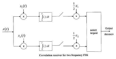
[0005] Figure 2 is a diagram of Correlation receiver for a two frequency FSK
of the
system of Figure 1;
[0006] Figure 3 is block diagram of an analog front end (AFE) of the system of
Figure 1;
[0007] Figure 4 is a schematic diagram of the AFE of Figure 3;
[0008] Figure 5 is a schematic diagram of a transmitter circuit of the AFE of
Figure
4;
[0009] Figure 6 is a schematic diagram of a low pass filter of the AFE of
Figure 4;
[0010] Figure 7 is a schematic diagram of a high pass filter of the AFE of
Figure 4;
[0011] Figure 8 is a schematic diagram of a protection circuit of the AFE of
Figure 4;
[0012] Figure 9 is a schematic diagram of a band pass filter and amplifier of
the AFE
of Figure 4;
[0013] Figure 10 is a schematic diagram of a high pass filter of the AFE of
Figure 4;
[0014] Figure 11 is a schematic diagram of a protection diode circuit of the
AFE of
Figure 4;
[0015] Figure 12 is a schematic diagram of a band pass filter and amplifier of
the
AFE of Figure 4;
[0016] Figure 13 is a schematic diagram of another low pass filter of the AFE
of
Figure 4;
[0017] Figure 14 is a schematic diagram of another band pass filter and
amplifier of
the AFE of Figure 4;
[0018] Figure 15 is a schematic diagram of a limiter of the AFE of Figure 4;
[0019] Figures 16 and 16a are schematic diagrams of an automatic gain control
amplifier of the AFE of Figure 4; and
[0020] Figure 17 is chart showing an optimized reception and transmission of
multiple frequencies using a sine wave for the system of Figure 1.
2
TDO-RED #8299833 v. I
CA 02528799 2005-12-01
DETAILED DESCRIPTION OF EMBODIMENTS
[0021] The description which follows, and the embodiments described therein,
are
provided by way of illustration of an example, or examples, of particular
embodiments of
the principles of the present invention. These examples are provided for the
purposes of
explanation, and not limitation, of those principles and of the invention. In
the
description, which follows, like parts are marked throughout the specification
and the
drawings with the same respective reference numerals.
[0022] Current high speed communication on power line media (e.g. standard in
house wiring) uses a variety of modulation techniques to overcome the highly
noisy
environment. Two types of systems have been commonly used. Firstly, wideband
systems that uses spread spectrum to combat the interference may be used, see
for
example:
5,574,748 and 5,090,024 - Spread spectrum communications system for network;
5,263,046 - Spread-spectrum chirp communication with sharply defined
bandwidth;
6,243,413 - Modular home-networking communication system and method using
disparate communication channels;
6,616,254 - Code shift keying transmitter for use in a spread spectrum
communications system;
5,579,335 - Split band processing for spread spectrum communications; and
5,748,671 - Adaptive reference pattern for spread spectrum detection,
the contents of which are hereby incorporated by reference.
[0023] Secondly, narrow band systems that use one or more frequencies
modulated in
frequency or phase may also be used. See for example:
5,504,454 - Demodulator for powerline carrier communications; and
4,475,217 - Receiver for phase-shift modulated carrier signals,
the contents of which are hereby incorporated by reference.
3
TDO-RED #8299833 v. 1
CA 02528799 2005-12-01
[0024] But Type of modulation techniques may also use various kind of
synchronization, see for example:
6,734,784 - Zero crossing based powerline pulse position modulated
communication system;
6,577,231 - Clock synchronization over a powerline modem network for multiple
devices;
6,784,790 - Synchronization/reference pulse-based powerline pulse position
modulated communication system;
6,907,472 - Distributed synchronization mechanism for shared communications
media based networks; and
5,553,081 - Apparatus and method for detecting a signal in a communications
system,
the contents of which are hereby incorporated by reference.
[0025] The type of system used is also a function of the frequency spectrum
allowed
in the country of use. Most countries do not allocate enough spectrum for the
wideband
spread spectrum systems, so narrowband systems have been favoured, see for
example:
- USA: FCC, PART 15 47 CFR CH.1 A, RADIO FREQUENCY DEVICES
(PART 15);
- EUROPE: EN50065-1 - SIGNALING ON LOW-VOLTAGE ELECTRICAL
INSTALLATIONS IN THE FREQUENCY RANGE 3 kHz TO 148.5
kHz; and
- CANADA: ICES-006, Issue 1, August 25, 2001, AC Wire Carrier Current
Devices (Unintentional Radiators),
the contents of which are hereby incorporated by reference.
[0026] One feature of all these systems is that they use continuous
transmission for
each message, where a message typically consists of 100's of bits. However it
has been
observed from a large sample of data from the field that the noise on typical
power lines
where a number of disturbing devices are connected is not constant in either
time or
frequency, but exhibits quiet periods in both dimensions. The transmission
system of the
4
TDO-RED #8299833 v. I
CA 02528799 2005-12-01
present invention thus uses both time and frequency diversity to improve the
robustness
of the system in the presence of large amounts of non stationary power line
noise, thereby
achieving significantly improved performance in very adverse conditions.
[0027] In an aspect of the present invention, the transmission system divides
the time
axis into a number of time slots synchronized such that one time slot starts
at the zero
crossing of the power line signal (50 or 60 Hz depending on the region). These
time slots
are called channels and numbered from 1 to n. The modulation method used is
narrow
band continuous phase FSK, where a number m of modulating frequencies are
used,
arranged such that an integral number of full cycles fit into each channel
time slot for all
m frequencies. The system transmits during only a subset of the available time
slots
(channels) concentrated near the zero crossing of the power line waveform
where the
noise is typically minimal.
[0028] The system uses diversity by transmitting the same bit over one or more
channels (time slots) and one or more frequencies. It uses a positive
acknowledgment
protocol with a reverse channel to tell the transmitter which redundancy
method to use at
any given time. The transmitter and receiver are both synchronized to the
power line
signal zero crossing and the default transmission method is the lowest bit
rate using the
maximum diversity. The system additionally uses a cyclic redundancy check
(CRC)
polynomial to detect the correct reception of messages - if the CRC is not
received
correctly, no acknowledgment is sent and the transmitter will revert to its
default high
redundancy state after some programmable delay.
[0029] In the paragraphs that follow, an embodiment of the system is described
using
a particular example of 4 channels and 2 frequencies on a 60 Hz power line.
However it
should be clear to anyone versed in the art that this can be readily expanded
to a n
channels and m frequencies as well as the use on other power line frequencies
(e.g. 50
Hz), in other embodiments.
TDO-RED #8299833 v. I
CA 02528799 2005-12-01
Burst mode FSK
[0030] Referring to Figure 1, tor the embodiment, the transmission method
chosen is
traditional FSK with two frequencies. The period of the power line waveform is
divided
into a number of segments, and transmission occurs during some but not all
these
segments. Thus consider segments of 600 sec - in a 60 Hz power line the
period is
16.67 msec and the half period is 8.33 msec, giving 14 time slots of 595 sec
in one half
period. Of these the system transmits in 4 timeslots of 600 sec , leaving the
rest of the
period empty. The 4 timeslots are arranged asymmetrically with one before the
zero
crossing and 3 after - this is illustrated in Figure 2 and are numbered as
channel 1 to 4.
[0031] The system of the embodiment uses continuous phase FSK with the
transmitted signals:
sm (t) = T cos(27rf.t + 27c m Of t) m=1,2
and Af chosen such that:
_k
~f T
which assures seamless switching at the end of the burst T. Choosing T 600
sec and:
70 =116.7 kHz
T
4f=~=16.7kHz
f2 =f,+Of=133.3kHz
completes the definition of the bursts. The receiver uses a traditional bank
of correlators
as shown in Figure 3. The correlators are synchronized to the zero crossing of
the power
6
TDO-RED #8299833 v. 1
CA 02528799 2005-12-01
line waveform and the output is sampled at the nearest peak at the end of the
period T,
minimizing the effect of any jitter in the zero crossing detection.
[0032] The cross correlation of these signals sampled at T is given by:
Pmk 1 f sm (t)sk (t) dt
2~
T
2~ f F32 cos(27r f~.t + 27c mOf t) =~ cos(2~ t + 2~ kOf t) dt
0
[0033] This equation has two parts, one at DC and the other at 2 times the
carrier
frequency f, The result of the integration of the two parts is:
1
pmk = T f cos(2;t( m- k)Of t) dt
0
T
+T f cos(47c ft + 2;t (m + k)Af t) dt
0
- sin(27c( m- k)Af T) + sin(47c fT + 27c (m + k)Af T)
2;r( m- k)Of T 41r fT + 2;r (m + k)Of T
=1 if m=k
= 0 otherwise
since we have chosen f, = T= 70 and Af = T = 10. Note that this correlation is
normalized to 1 because we divided it by the signal power. This also gives a
clue about
the effect of jitter in the zero crossing mentioned above. In this case the
correlation is
over a shorter period, resulting in less energy at the output. If we
synchronize the
correlator by taking the largest output sample near the end of the original
burst, the effect
can be approximated as the ratio the reduced burst length due to jitter Tred
to the original
burst length T as shown below:
7
TDO-RED #8299833 v. 1
CA 02528799 2005-12-01
Pmk 2s e S. (t)Sk (t) dt
Ted
cos(2;z f t+ 2~ kAf t) dt
1 FLT cos(2~ f t+ 2~ mOf t) FLT
=2s f '
-
TYed sin(2;r( m- k)OfT,ed )+ sin(4;T fT + 27c (m + k)Of Tred )
T 27C( m- k)Af TPed 47c f T+ 2;z (m + k)Of Tred
=T~ed ifm=k
T
= 0 otherwise
where we have assumed that TYed = fe and Tred = Af are still integers (this
just says that
we correlate over an integral number of cycles of fl and f2).
Transmission methods using time and frequency diversity
[0034] The four time slots may be viewed as four independent channels. Thus
diversity techniques are used to improve robustness in the presence of noise.
In
particular we use both time and frequency diversity by transmitting multiple
copies on
different channels and using one or two frequencies as further explained
below. Various
combining techniques are then used to improve the robustness of the detection.
[0035] For the embodiment, the following transmission methods A - E may be
used
in this case, although this list is not exhaustive, and more possibilities
exist particularly in
the case of more channels and more frequencies:
A. (480bps).2-frequencies. 1-bit per channel. 4-bits per burst.
B. (240bps).2-frequencies. 2-bits per burst, Channel 0 and 1 merged. Channel
2 and 3 merged
C. (120bps).2-frequencies. 1-bit per burst, Channel 0 and 1 merged. Channel
2 and 3 merged. a '0' is a transition from F 1 to F2, a '1' is a transition
from F2 to
Fl
D. (120bps).2-frequencies. 1-bit per burst, All Channel Merged
8
TDO-RED #8299833 v. I
CA 02528799 2005-12-01
E. (60bps).2-frequencies. 1/2-bit per burst, All Channel Merged, a'0' is a
transition from Fl to F2, a' 1' is a transition from F2 to Fl
[0036] These are illustrated graphically in the following tables 1 to 5:
Burst 1
bO bl b3 b4
Table 1 Method A
Burst 1
bO bO bl bl
Table 2 Method B
Burst 1
Fl Fl F2 F2
0
F2 F2 Fl Fl
1
Table 3 Method C
Burst 1
bO bO b0 bO
Table 4 Method D
Burst 1 Burst 2
Fl F1 Fl Fl F2 F2 F2 F2
0
F2 F2 F2 F2 Fl Fl Fl Fl
1
Table 5 Method E
Detection algorithms using time and frequency diversity
[0037] For the embodiment, the detector uses time and frequency diversity
methods
to improve the robustness of the transmission. The 4 channels and the 2
frequencies are
used to make a combined decision depending on the transmitted sequence. The
receiver
9
TDO-RED #8299833 v. 1
CA 02528799 2005-12-01
monitors the channel and makes a decision on which transmission method is
likely to
yield the best result. A reverse channel protocol is used to communicate this
decision to
the transmitter.
[0038] Outlined below are some of the detection methods that can be used used,
although it will be appreciated that this list is not exhaustive and other
additional methods
may also be used as is evident to anyone versed in this art. The basic idea is
to use time
diversity first by either repeating the same information in a number of time
slots or
reducing the number of time slots used, ignoring the ones that are too noisy.
This is then
combined with frequency diversity by using only one of the two frequencies to
make the
decision, ignoring the other one judged to be too noisy. In the general case
we use k out
of n time slots and 1 out of m frequencies.
[0039] Method A:
1. Use maximum likelihood decision from correlator
[0040] Method B
1. Use maximum likelihood decision from correlator on merged channels
2. Use maximum likelihood decision from correlator only on merged channels 1,2
[0041] Method C
1. Use maximum likelihood decision from correlator on merged channels 1,2 and
3,4
then apply differential decoding
2. Use maximum likelihood decision from correlator only on merged channels 1,2
then apply differential decoding
3. Same as 1 or 2 but monitor only change in F1
4. Same as 1 or 2 but monitor only change in F2
TDO-RED 48299833 v. I
CA 02528799 2005-12-01
[0042] Method D
1. Use maximum likelihood decision from correlator on merged channels 1,2,3,4
2. Use maximum likelihood decision from correlator only on merged channels 1,2
3. Use maximum likelihood decision from correlator only on channel 1
4. Use maximum likelihood decision from correlator only on channel 2
[0043] Method E
1. Use maximum likelihood decision from correlator on merged channels 1,2,3,4
in
burst 1 and burst 2 and apply differential decoding
2. Use maximum likelihood decision from correlator only on merged channels 1,2
in
burst 1 and burst 2 and apply differential decoding
3. Use maximum likelihood decision from correlator only on channel 1 in burst
1 and
burst 2 and apply differential decoding
4. Use maximum likelihood decision from correlator only on channel 2 in burst
1 and
burst 2 and apply differential decoding
5. Same as 1 to 4 but monitor only change in F 1
6. Same as 1 to 4 but monitor only change in F2
Synchronization, startup and tracking
[0044] For the embodiment, the system uses a simple link layer protocol for
startup
and tracking. Synchronization is achieved by detecting the zero crossing of
the power
line signal and then looking for the maximum of the larger correlator output
to determine
the end of the burst near T micro seconds after the zero crossing (note that
the correlator
will contain part of the second burst if the zero crossing is detected late or
noise only if it
is detected early due to jitter , but the effect of this is small as shown
above).
[0045] The link layer protocol transmits messages bounded by a start of
message
sync pattern at the beginning and a CRC at the end of the message. The
receiver uses this
11
TDO-RED #8299833 v. 1
CA 02528799 2005-12-01
CRC to determine if correct operation has been achieved and sends a positive
acknowledgement to the transmitter to that effect.
[0046] It should be noted that other link layer protocols may also be used in
conjunction with the transmission system in other embodiments, as will be
evident to
anyone versed in this art.
[0047] Startup is achieved by transmitting at the lowest bit rate, ('/2 bit
per burst in
this case). Once successful transmission at this bit rate is achieved (correct
CRC
received), the receiver monitors all channels and all frequencies to determine
if a higher
bit rate could be sustained. It then communicates to the transmitter via a
control message
to use one of the other transmission patterns and switches its detection
algorithm
accordingly. It should be noted that another implementation can start with the
highest bit
rate and reduce it in case of bad CRC. Improved robustness is achieved by
positively
acknowledging each message. This allows the transmitter to revert to the
lowest bit rate
in case the channel deteriorates to the point where the receiver is not
receiving correct
data and does not send an acknowledgement.
Analog Front End Requirements
[0048] The analog front end (AFE) is an analog circuit composed of a
transmission
and a reception circuit. This circuit provides the connection from the digital
signal
processing portions of the system to the analog portion of the power line. The
receiver
circuit is always on, whereas the transmitter circuit must be enabled with a
logical high
(1) on the TX_Enb pin. Both circuits have a protection diode circuit to limit
spikes and
signals present on the powerline and pass through the coupling.
[0049] Referring to Figure 3, a simplify block diagram of the AFE is shown.
Referring to Figure 4, a circuit schematic showing additional details of the
AFE is shown.
[0050] For the embodiment, the following provides a summary of different
filters that
may be used in the AFE:
12
TDO-RED #8299833 v. I
CA 02528799 2005-12-01
D 1 1 '
Filter 1 Characteristics
Filter type Butterworth Low-Pass
Order 4
Cut off Frequency 180 KHz -3 dB
Filter 2 Characteristics Butterworth High-Pass
Filter type
Order 2
Cut off Frequency 190 KHz -3 dB
Filter 3 Characteristics
Filter type (Type) Band-Pass
Order for the high pass 10
Order for the low pass 4
Cut off Frequency (Low) 106 KHz -6 dB
Cut off Frequency (High) 160 KHz -6 dB
Frequency Center 125 KHz
Gain 20dB
AGC Characteristics
Gain >30dB
Response delay 30 S
Power Amplifier
Characteristics
Input impedance 60052
Output impedance <1 S2
Gain l 1 1 dB
Bandwidth 80-150KHz
Power 2.25Wpeak (3Vpeak in 40)
Protection Short circuit and over Protected by coupler
voltage impedance
Distortion -60dB (3' harmonic) Output impedance: 5052
Table 6 - AFE Specifications
[0051] Details regarding different aspects of the AFE are now described in
turn.
Transmitter Circuit
[0052] Referring to Figure 5, the amplifier section of the AFE is made up of
two
stages:
= The transmission filter (TX filter).
13
TDO-RED #8299833 v. 1
CA 02528799 2005-12-01
= A voltage/current stage amplifies the input signal with low-distortion to
meet
FCC, ICES and CENELEC requirements. The output stage haslow output
impedance. The amplifier is controlled by the Tx_Enb signal. When Tx_Enb is
low, the current stage is high impedance to allow power line signal to be
received
by the RX section. When Tx_Enb is high, the current stage amplifies the signal
from the voltage amplifier and transmits it to the coupler.
[0053] The amplification is 11 1 dB. So the range is 1.7 volts peak-to-peak.
The
output impedance is less than 1 Q when transmitting and more than 250 S2 in
idle state.
The transmitter uses an integrated circuit to simplify the amplification. The
integrated
circuit amplifier supports low impedance on the power line without distorting
the signal
transmission.
[0054] For the embodiment, a 2 amplifiers that work with a bridge
configuration to
be able to transmit a 6Vpp signal on the line from a single 5V supply is used.
The output
of the transmission amplifier is not protected against shorts between ground
and output.
The output signal is transmitted at 6 Vpp for a load greater than 6 Q. For a
load smaller
than 6 S2, the output signal decreases but the distortion stays at a low level
to avoid
transmitting harmonics on the power line.
[0055] The band-pass filter of the amplifier ranges from 80 kHz to 150 kHz. As
the
RHINO IC delivers a pulse witdh modulation signal, we need to filter it by
using a passif
low pass filter to reshape the signal to amplify. The transmitting filter is
used to filter the
signal taken from the RHINO IC and to feed it to the voltage/current
amplifier. This is
accomplished by eliminating the high frequencies of the TX signal at the input
of the
amplifier. This may be done by a low pass filter as shown in Figure 6.
Receiver Circuit
[00561 For the embodiment, the receiving circuit is always enabled. It
receives the
signal from the power line and filters it for the RHINO IC. The receiver have
several
functions to achieve for the RHINO IC:
14
TDO-RED #8299833 v. I
CA 02528799 2005-12-01
- Extract the signal of the noise present at the output of the coupling
circuit by a
efficiency filtering
- Compress the signal without clipping it to preserve the shape when the
maximum amplitude is reached
- Amplify the signal when it is necessary; depending of the attenuation
present
on the powerline
- Warm the RHINO IC as it compress the signal and when the line is noisy
[0057] To do these functions, the receiver is divided in several sections
which are
independent of each other. Depending of performances required for different
commercial
applications, this division provides an easy ability to remove sections. For
the
embodiment, the following sections are implemented:
- A high pass filter
- A protection diode circuit - A band-pass filter and amplifier
- A high pass filter
- A protection diode circuit
- A band-pass filter and amplifier
- A low pass filter
- A band-pass filter and amplifier
- A limiter that react as a protection for the RHINO IC
- an automatic Gain Control amplifier which control gain of 2 of the three
amplifiers
[0058] The different sections clean the signal but do not saturate it to
preserve the
shape of the signal. The minimum signal to be detected by the AFE is 30 V if
the noise
floor is lower than -97 dB (Vpp). This gives a sensitivity of -97 dB.
[0059] Each of these sections are now described in turn. Referring first to
Figure 7, a
high pass filter is shown.
[0060] Referring to Figure 8, a protection diode circuit is shown.
TDO-RED #8299833 v. I
CA 02528799 2005-12-01
[0061] Referring to Figure 9, a band-pass filter and amplifier is shown.
[0062] Referring to Figure 10, a high pass filter is shown.
[0063] Referring to Figure 11, a protection diode circuit is shown.
[0064] Referring to Figure 12, a band-pass filter and amplifier is shown.
[0065] Referring to Figure 13, a low pass filter is shown.
[0066] Referring to Figure 14, a band-pass filter and amplifier is shown.
[0067] Referring to Figure 15, a limiter that react as a protection for the
RHINO IC is
shown.
[0068] Referring to Figures 16 and 16a, an automatic gain control (AGC)
amplifier
that controls gain of 2 of the three amplifiers is shown.
100691 The AGC is designed to have fast response within 80 S. This is enough
fast
to control amplification of the different section of the receiver and gives
feedback to the
RHINO IC.
[0070] Referring now to Figure 17, an optimized reception and transmission of
multiple frequencies using a single sine wave is now described and shown. As
shown,
there is a 356pts 2.5khz sine wave stored in RAM memory (for a sampling rate
of
888888.8 samples per seconds). This single sine wave is used by the DSP to
perform
DTFT on any frequency that is a multiple of 2.5khz.
[0071] The following function performs the DTFT at 110khz using this table.
Notice
that only N register must be modified in order to select any frequency.:
moveu.w #356,LC // 2c
moveu.w #(32768 + 356-1),M01 // RO and Rl are configured as MOD(356)
Addressing
move.w #44,N // 44 x 2.5khz = 110khz parameter
moveu.w #DFTTable + 89,R0 // Imaginary Part (Cos) offset of 90degrees
moveu.w #DFTTable,Rl Real Part (Sin) no offset
moveu.w #TestBuffer,R3 ADC Data Ptr
clr a x:(rl)+N,yl // real part+ add(N) to rl
nop
clr b x:(r0)+N,yO x:(r3)+,x0 // imaginary part+ add(N) to rO
DOSLC _ENDOFLOOP
16
TDO-RED #8299833 v. 1
CA 02528799 2005-12-01
mac yl,xO,a x:(rl)+N,yl // real part + add(N) to rl
mac yO,xO,b x:(rO)+N,yO x:(r3)+,xO // imaginary part + add(N) to rO
ENDOFLOOP:
[0072] It will be appreciated that the same principles may be used in
transmission in
order to generate a pulse width modulated wave.
[0073] Although the invention has been described with reference to certain
specific
embodiments, various modifications thereof will be apparent to those skilled
in the art
without department from the scope of the invention.
17
TDO-RED #8299833 v. I