Note: Descriptions are shown in the official language in which they were submitted.
CA 02528889 2009-05-12
IJ.S. NON-PROVISIONAL PATENT APPLICATION
TITLE OF THE INVENTION
[0001) Environmental Protection of Serial ATA and Other Electronic Devices
BACKGROUND OF THE INVENTION
100031 The present invention relates oenerally to systems for the
environmental protection of
senat ATA a1id other electronic devices and, more particularly, to advanced
tecluuques for
providing communication and coufigtiring the operation of such envii-
onmentally protected
devices.
[0004) Serial Advanced Technology Attac}u ent (SATA) provides an interface to
attach
peripheral and othcr e]ecti-onic devices to host computei-s or other host
devices_ There is a need to
install SATA devices or host devices into harsli envirortrnents that exceed
the design and operating
parameters of the SATA devices or host devices_ SATA presents design
challenges in providing
environmental protection while inaintaining a simple and reliable host to
device interface. The
present invention provides a cost effective solution for such challenges.
[0005) Peripheral and other devices operating in harsh environments, such as
within the
equipment bay of an aircraft, are typically enclosed within a sealed vessel
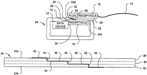
that provides a
temperatui-e controlled, dry, constant pressure atmosphere for the device. The
peripheral oi- other
device may also be protected with other systems such as vibration isolators or
the like. The
pr-otection system is nionitoi-ed and conti-olled with the objective of
maintaining the environment
within the operational i-ange of the peripheral or other electronic device and
to disable ttie device if
that objective cannot be met_
[0006) The preseni invention resolves tvvo major issues present in
environinentally protecting
electronic devices: (a) providing reliable electrical cojmectivity between a
SATA host or other
host device and the SATA or other electronic device while maintaining at least
one device in a
-1-
CA 02528889 2005-12-08
WO 2005/002121 PCT/US2004/019649
temperature controlled, pressurized, dry environment and (b) assuring that the
SATA device is only
active when the environmental conditions within the sealed vessel are
maintained within the
operational range of the SATA or other electronic device.
[0007] Serial ATA is presented as an example of a modern high-speed electrical
interface. The
SATA standard is designed to optimize the perfonnance/price ratio.
Optimization is partly
accomplished by leaving only a small margin for signal degradation within the
cabling and
connectors used for sending signals to and receiving signals from the SATA
device. Such a small
signal degradation margin requires imiovation when transmitting electrical
signals at 3 GHz. The
SATA standard addresses this by specifying twinax cables (shielded
differential lines). This type
of cable or any other high-speed impedance controlled solution is difficult to
feed into a seal
vessel.
[0008] Hermetically sealed connectors are the classic solution used to feed
electrical signals
into a sealed vessel that contains electronic equipment: Such sealed
comiectors are expensive and
offer primarily basic pin and socket electrical contacts that present a risk
of Radio Frequency (RF)
emission and susceptibility problems. Sealed twinax connectors are a better
electrical solution but
are rare and expensive. The present invention utilizes specific printed
circuit materials, conductive
trace and via routing techniques, and sealing methods to create a pressure and
moisture barrier that
is capable of conducting the electrical signals into and out of a sealed
environmentally controlled
vessel. These materials and techniques resolve normal Printed Circuit Board
(PCB) and flexible
printed circuit leakage caused by both porous barrels of plated vias and
moisture permeable
laminate materials. The invention is applicable to any electronic device but
is especially useful for
high frequency signals such as those associated with SATA devices.
[0009] The second issue addressed by the present invention is to assure that
the SATA device
only operates when specified environmental conditions are met. This is
typically accomplished in
the prior art by removing power to the SATA device or requesting the SATA host
to not
cominunicate over the SATA PHY (Physical layer) interface. Such solutions
require specialty
power supplies or customized host software. The present invention accomplishes
the same result
by incoiporating a PHY block circuit between the SATA device within the sealed
environmentally
protected vessel and the SATA host that disrupts communication over the
interface. The PHY
block circuit is controlled out-of-band by an environmental controller which
monitors the
environmental parameters such as temperature, pressure, etc. within the sealed
vessel. The
environmental controller has independent control over the operational state of
the SATA device
since, per the SATA specification, the device is inactive if the PHY interface
is not established.
-2-
CA 02528889 2005-12-08
WO 2005/002121 PCT/US2004/019649
SUMMARY OF THE INVENTION
[0010] Briefly, stated the present invention, in one embodiment, comprises a
system for
communicating with an electronic device within a sealed vessel, comprising a
generally enclosed
housing having an opening. A printed circuit board, fabricated using special
materials and
techniques, covers the housing opening to create a fully enclosed, sealed
vessel. An electronic
device is located within the interior of the sealed vessel and an external
device, such as a host
device is located outside of the sealed vessel. At least one conductive path
extends through the
printed circuit board from a first surface located outside of the sealed
vessel to a second surface
located inside of the sealed vessel. The at least one conductive path has a
first end on the first
surface which is connected to the external device and a second end on the
second surface which is
connected to the electronic device within the sealed vessel. In this manner, a
communication path
is established between the external device and the electronic device within
the interior of the sealed
vessel utilizing the at least one conductive path.
[0011] In another embodiment, the present invention comprises a system for
communicating
with an electronic device within a sealed vessel comprising a generally
enclosed housing having an
opening. A printed circuit board or flexible printed circuit, fabricated using
special materials and
techniques, extends through the housing opening so that a first portion of the
printed circuit
extends out of the housing and a second portion of the printed circuit extends
into the housing. The
printed circuit includes first and second surfaces which are sealed to the
housing to create a fully
enclosed, sealed vessel. An electronic device is located within the interior
of the sealed vessel and
an external device is located outside of the sealed vessel. The at least one
conductive path extends
along the interior of the printed circuit between the first and second
portions. At least one
conductive path has a first end on one of the surfaces of the first portion of
the printed circuit
connected to the external device and a second end on one of the surfaces of
the second portion of
the printed circuit connected to the electronic device. In this manner, a
communication path is
established between the external device and the electronic device within the
interior of the sealed
vessel utilizing the at least one conductive path.
[0012] In yet another embodiment the present invention comprises a system for
coinmunicating
with a SATA device within a sealed enviromnentally controlled vessel. The
system includes a
sealed vessel having an environmentally controlled interior with a SATA device
within the interior
of the sealed vessel. A host device is located outside of the sealed vessel
and a communication
path extends between the host device and the SATA device within the interior
of the sealed vessel.
An environmental controller monitors at least one enviromnental condition
within the sealed
-3-
CA 02528889 2005-12-08
WO 2005/002121 PCT/US2004/019649
vessel, compares the monitored environmental condition to a predetermined
standard and generates
output signals. A physical layer blocker circuit is connected to the
environmental controller and to
the communication path between the host device and the SATA device. The
pliysical layer blocker
circuit receives the output signals from the environmental controller, enables
the coinmunication
path when the monitored environmental conditions meet the predetermined
standard and disables
the communication path when the monitored environmental condition does not
meet the
predetermined standard.
BRIEF DESCRIPTION OF THE SEVERAL VIEWS OF THE DRAWINGS
[0013] The foregoing summary, as well as the following detailed description of
preferred
embodiments of the invention, will be better understood when read in
conjunction with the
appended drawings. For the purpose of illustrating the invention, there are
shown in the drawings
embodiments which are presently preferred. It should be understood, however,
that the invention
is not limited to the precise arrangements and instrumentalities shown.
[0014] In the drawings:
[0015] Fig. 1 is a schematic diagram illustrating the problem involved with
sealing an
electrical interface as it enters a closed vessel; especially when the cable
is of twinax construction;
[0016] Fig. 2 is a schematic diagram illustrating a first preferred embodiment
of the present
invention in wliich a printed circuit board is used to enclose and seal a
vessel containing a device;
[0017] Fig. 3 is a greatly enlarged sectional view of the printed circuit
board of Fig. 2
showing the path of a conductive trace;
[0018] Fig. 4 is a view similar to that of Fig. 3 illustrating a first
alternative embodiment for
the conductive trace of the printed circuit board;
[0019] Fig. 5 is a view similar to that of Fig. 3 but illustrating a second
alternative
embodiment of the conductive trace of the printed circuit board;
[00201. Fig. 6 is a view similar to that of Fig. 3 but illustrating a third
alternative embodiment
of the conductive trace of the printed circuit board;
[0021] Fig. 7 is a view similar to that of Fig. 3 but illustrating a fourth
alternative embodiment
of the conductive trace of the printed circuit board;
[0022] Figs. 8 and 8a are views similar to that of Fig. 3 but illustrating a
fifth alternative
embodiment of the conductive trace of the printed circuit board in side
section and end section;
[0023] Fig. 9 is a schematic view of second preferred embodiment of the
present invention in
which the printed circuit board extends into and out of the sealed vessel;
-4-
CA 02528889 2005-12-08
WO 2005/002121 PCT/US2004/019649
[0024] Fig. 10 is a schematic view of third embodiment of the present
invention in which a
specialized cable is used instead of a printed circuit board;
[0025] Fig. 11 is a schematic representation of a PHY blocker circuit in
accordance with the
present invention; and
[0026] Figs. 12a and 12b, 12c and 12d illustrate alternative embodiments of
the detailed
structure of the PHY blocker circuit of Fig. 11.
DETAILED DESCRIPTION OF THE INVENTION
[0027] Referring to the drawings wherein like numerals are used to indicate
like elements
throughout the several figures, there is shown in Fig. 1 an external device,
in the present
embodiment a host 10 electrically connected to a device 12 with a cable 14.
The cable 14 has a
connector receptacle 16 on each end that plugs directly into compliineiitary
connectors or plugs
(not shown) integral to the host 10 and device 12. Power for the device 12 is
provided by way of a
separate cable that has been omitted from all of the drawings for simplicity.
A housing 18
surrounds the device 12 and includes an opening 20 through which the cable
passes. A simple seal
22 around the cable 14 does not create a moisture and airtiglit seal since the
cable interior wires
and shields create multiple egress paths. This is especially tr-ue of cable
using shield twisted pair or
twinax construction. It should be understood that while in the present
embodiment the external
device is the host 10, the host 10 could be within the housing 18 and the
electronic device 12 could
be the external device.
[0028] Fig. 2 illustrates a first embodiment of the present invention in which
a printed circuit
board (PCB) 24 is used with a conventional housing 18 to create a sealed
vesse126. The PCB 24 is
sealed to the housing 18 to fully cover the opening 20 utilizing a moisture
blocking sealant 28 such
as PRC-Desoto PR-1440, a sealing 0-ring or some other suitable sealing device
or technique. If
RF einissions or reception control is required an electrically conductive
sealant such as
PRC-Desoto PR-1564 is used to extend the shield to the housing 18. Preferably,
the PCB 24 is
formed by one or more substrate layers of air impermeable, low moisture
absorbance material such
as Park Nelco N-5000.
[0029] The PCB 24 includes at least one and preferably two or more conductive
paths 30 (only
one shown) extending through the PCB 24 from a first surface 24a located
outside of the sealed
vessel 26 to a second surface 24b located inside of the sealed vessel 26. The
conductive path 30
has a first end 32 on the first surface of the PCB which is used for
connecting througha suitable
plug 34 and the receptacle 16 to the external device or host 10. The
conductive path 30 further
-5-
CA 02528889 2005-12-08
WO 2005/002121 PCT/US2004/019649
includes a second end 36 on the second PCB surface 24b connected to the device
12 utilizing the
receptacle 16. In this maimer, the conductive path 30 is used to provide an
airtight, moisture tight
connection extending through the PCB 24 for connecting the host 10 to the
device 12 within the
environmentally controlled interior of the sealed vessel 26 without adversely
affecting the sealed
nature of the vessel 26 or the protective environment within the sealed vessel
26.
[0030] Fig. 3 is an enlarged schematic cross sectional view of a first
einbodiment of a PCB 24
of the type employed for enclosing the housing 18 to create the sealed vessel
28 as shown in
Fig. 2. Only a single conductive path 30 is shown in Fig. 3 for the sake of
brevity. However, it
will be appreciated by those of ordinary skill in the art that two or more
conductive paths 30 may
be provided for making all of the necessary electrical connections. The
conductive path 30 as
shown in Fig. 3 is comprised of seven conductive elements which as described
below are
connected together, at least electrically, to fonn a complete conductive path
from the first PCB
surface 24a to the second PCB surface 24b. In the embodiment illustrated in
Fig. 3, the PCB 24 is
formed of three laminated layers of substrate material 36, 38 and 40 with the
exposed surface of
the first substrate layer 36 forming the PCB outer surface 24a and the exposed
surface of the third
substrate layer 40 forming the PCB inner surface 24b. A greater or lesser
nuinber of PCB substrate
layers may be employed for particular applications. A first conductive trace
element 42 is located
on the exposed surface of the first PCB substrate layer 36 and extends
generally parallel to the first
PCB surface 24a. The first conductive trace element 42 is connected to the
plug 34 on the first
PCB surface 24a. The second conductive element is a blind via 44 which has a
first end connected
to the first trace element 42 and extends completely through the first PCB
substrate layer 36. The
third conductive element is a conductive trace 46 which is connected to the
second end of the blind
via 44 and extends within the area between the first and second PCB substrate
layers 36, 38 and
generally parallel to the first PCB surface 24a. The fourth element is a
buried via 48 which has a
first end connected to conductive trace element 46 and extends through the
second PCB substrate
layer 38. The fifth element is a conductive trace 50 which is connected to the
second end of the
buried via 48 and extends along the second substrate layer 38 and generally
parallel to the first
PCB surface 24a. If the PCB 24 contains only two substrate layers 36, 38 then
the fifth conductive
trace element 50 would be on the second PCB surface 24b for connection to the
device 12.
However, in the embodiment shown in Fig 3, the PCB 24 includes three substrate
layers 36, 38
and 40. Accordingly, a sixth conductive trace element is another blind via 52
which extends
through the third PCB substrate layer 40 with a first end connected to
conductive trace element 50.
A seventh element is a conductive trace 54 which is connected to a second end
of the blind via 52
-6-
CA 02528889 2005-12-08
WO 2005/002121 PCT/US2004/019649
and extends along the exposed surface of the third PCB substrate layer 40. In
the embodiment
shown in Fig. 3, the seventh conductive element is connected to the receptacle
16 associated with
the device 12. By forming the conductive path 30 with multiple types of
interconnected trace and
via elements, the integrity of the sealed vessel 26 is maintained since the
horizontal sections
provide sealing and the vertical sections migrate the comiection between the
first PCB surface 24a
and the second PCB surface 24b. Preferably, the PCB substrate layers 36, 38
and 40 are fused
during the lainination process to provide a tight seal around the various
conductive trace elements
there between. Preferably, a lamination technique using heat and pressure cure
of B-stage outer
substrate layers 36 and 40 fused to the A-stage inner core substrate layer 38
is employed to avoid
the use of adhesives that could potentially introduce a path for gas leakage
or moisture absorption
into or out of the sealed vessel 26.
[0031] There are times when a through-via may be advantageous despite the
potential
introduction of a path for fluid leakage around the barrel of the via. Fig. 4
illustrates a first
alternate embodiment of the PCB 24 of Fig. 2 which makes the use of a through
via 56 which
extends completely through the PCB 24 from the first or outer surface 24a to
the second or inner
surface 24b. The through via 56 essentially takes the place of the blind via
52 as shown in Fig. 3.
At least one end of the through via 56 in the present embodiment the end
proximate to the first
PCB surface 24a is sealed utilizing a generally circular sealing member 58 of
sealant material.
Importantly, the path of electrical conduction does not pass through the
sealing member 58, but
instead travels from the first PCB surface 24a to the second PCB surface 24b
through the various
conductive trace and via elements 42, 44, 46, 48, 50 and 54 utilizing only a
portion of the through
via 56 to interconnect conductive elements 50 and 54. The sealing member 58 is
sufficient to
protect the integrity of the sealed vessel 26. If desired, the sealing member
58 could be placed on
the second PCB surface 24b or sealing members could be used on both PCB
surfaces 24a and 24b
to cover both ends of the through via 56. Again, the purpose of the sealing
member 58 is to make
sure that the sealed vessel 26 remains airtight to protect the controlled
environment interior within
the sealed vessel 26.
[0032] Fig. 5 is an enlarged sectional view of another alternative embodiment
of a PCB 24 in
accordance with the present invention. The PCB 24 of Fig. 5 is substantially
the same as that of
Fig. 4 including a through via 56 and the various conductive trace and via
elements 42, 44, 46, 48,
50 and 54. As with the embodiment shown in Fig. 4, the through via 56 is used
to connect
together conductive trace element 50 and conductive trace element 54. However,
unlike the
embodiment shown in Fig. 4, the through via 56 is filled and at least one end
of through via 56
-7-
CA 02528889 2005-12-08
WO 2005/002121 PCT/US2004/019649
includes a sealing member 58. In the present embodiment, the sealing member 58
is fonned by
copper plating the first PCB surface 24a with a generally circular copper
land. If desired, the
sealing member 58 could be bonded on the second PCB surface 24b or sealing
members 58 could
be on both the first and second PCB surfaces 24a and 24b. Again, the sealing
member 58 seals any
opening in the PCB 24 resulting fiom the through via 56 in order to maintain
the sealed condition
of the sealed vessel 26 and the protected environment therein. The sealing
member 58 may be
installed on either or both of the PCB surfaces 24a and 24b utilizing
tecluiiques well known by
those of ordinary skill in the art. Although the sealing member 58 is
preferably made of copper, it
will be apparent to those of ordinary skill in the ar-t that the sealing
member 58 could be made of
other metallic or non-metallic materials if desired. As with the embodiment
shown in Fig. 4, the
through via 56 in combination with the various conductive trace and via
elements 42, 44, 46, 48 50
and 54 forms a complete conductive path through the PCB 24.
[0033] Fig. 6 is a side view of a further alternate environment of the present
invention. In the
embodiment shown in Fig. 6 the principal conductive path through the PCB 24 is
attained by the
through via 56 which extends completely through the PCB 24 constructed with
one or more
substrate layers. However, unlike the above-described embodiments, no
labyrinth of
intercoimected conductive trace and via elements is provided. Instead, only a
first conductive trace
element 42 extends along the first PCB surface 24a and is in electrical
contact with the conductive
sealing member 58 installed on the first PCB surface 24a over the through via
56. The sealing
member 58 is larger in diameter than the via hole and is bonded to the
substrate, forming a seal
over the potentially leaky via. Similarly, a conductive trace element 54 is
installed on the second
PCB surface 24b in electrical contact with the through via 56. If desired, a
sealing member 58
could be installed on the second PCB surface 24b or on both PCB surfaces 24a,
24b. The sealing
member 58 prevents any lealcage through the PCB 24 around the through via 56
to maintain the
integrity of the sealed vessel 26.
[0034] Fig. 7 is a sectional view of yet another embodiment of the present
invention. The
embodiment shown in Fig. 7 is also similar to that of Figs. 4 and 5. However,
unlike the
previously described embodiments, in Fig. 7 a generally circular plated
through hole 60 extends
coinpletely through the PCB 24 from the first surface 24a to the second
surface 24b. The through
hole 60 is fonned utilizing techniques well known to those of ordinary skill
in the PCB art. A
conductive pin member 62 is positioned within the through hole 60 and extends
slightly beyond the
PCB surface 24a and is connected to a plug 34. The second end of the
conductive member 62 as
well as the opening of the through hole 60 on the second PCB surface 24a is
covered by a sealing
-8-
CA 02528889 2005-12-08
WO 2005/002121 PCT/US2004/019649
member 58 formed of a sealant material of the type described above. Preferably
the pin member is
soldered to the plated hole 60 so that the solder forms a tight seal for the
interior of the via
barrel 60 and the exterior of the barrel is sealed by plating from the barrel
to one or more sealing
rings 59 (between substrate layers 38 and 40) or sealing members 58 extending
beyond the barrel
and bonded to the substrate layers of the PCB. The electrical path through the
PCB 24 is achieved
utilizing the conductive member 62 as well a various conductive trace and via
elements 46, 48, 50,
52 and 54 in the manner as described above. The sealing member 58 and/or
sealing rings 59
maintain the integrity of the sealed vessel 26. It will be apparent that other
configurations of
conductive trace elements and vias and the like either alone or in combination
may be used to form
' 10 electrical connections through the PCB 24 while maintaining the integrity
of the sealed vessel 26.
[0035] Figs. 8 and 8a illustrate, in further detail, an embodiment of the
present invention in
which four separate signal paths, two for transmit and two for receive are
provided by separate
parallel conductive paths 30 extending through the PCB 24 in a maiuier similar
to that described
above. Each conductive path 30 is comprised of a plurality of individual
conductive trace and via
elements 42, 44, 46, 48 and 54 as shown in Fig. 8 with each of the conductive
elements being in
parallel as illustrated by Fig. 8a. In addition, the transmit conductive
elements and the receive
conductive elements are each surrounded within the PCB 24 by ground planes 64,
66, 70 which are
also formed by a series of labyrinth conductive trace and via elements shown
generally as 68 and
70. This embodiment of the present invention the PCB 24 is comparable to a
grounded sealed
connector since both the transinit conductors and the receive conductors are
in proximity of the
respective ground planes 64, 66, 70. In this manner, the transmission path
through the PCB 24 is
free of leaks but yet also contains necessary shielding around the signal
conductors.
[0036] Fig. 9 shows a further alternate einbodiment of the present invention
in which the
PCB 24 is secured within the opening 20 of the housing 18 with a different
orientation. As shown
in Fig. 9, the PCB 24 extends through the housing opening 20 so that a first
portion 24c of the
PCB 24 extends out of the housing 18 and a second portion 24d of the PCB 24
extends into the
housing 18. The first and second PCB surfaces 24a, 24b include sealing
adhesive 28 in the vicinity
of the housing opening 20 in order to seal the opening 20 and create the
sealed vessel 26. At least
one conductive path 72 extends along the interior of the PCB 24 between the
first and second
portions 24c, 24d. In particular, the conductive path 72 is fonned by a first
via 74 extending from
the first PCB surface 24a through the first PCB substrate layer 36. A
conductive trace element 76
is connected to the via 74 and extends generally parallel to the first PCB
surface 24a in the area
between the first and second PCB substrate layers 36, 38. A second via 78 is
connected to the
-9-
CA 02528889 2005-12-08
WO 2005/002121 PCT/US2004/019649
conductive trace element 76 and extends through first PCB substrate layer 36
to the first PCB
surface 24a. The connector or receptacle 16 is connected to via 78 and the
plug 34 is connected to
via 74 to thereby complete the path along the PCB 24 and through the housing
opening 20. If
desired, the connector receptacle 16 and/or the plug 34 could be located on
the second PCB
surface 24b. The einbodiment disclosed in Fig. 9 provides all of the
advantages of maintaiiiing the
sealed vessel 26 in its airtight condition since the arrangement of the
conductive path 72 is free of
any gas or moisture leakage.
[0037] Fig. 10 illustrates yet a further embodiment of the present invention
in which a flexible
printed circuit 24' is employed in place of the PCB 24. The flexible printed
circuit 24' employs
routing and construction which is similar to that of the PCB embodiments
described above, except
the substrate layer is constructed using a flexible material such as etched
Teflon.
[0038] As previously noted, it is desirable to have the ability to
conveniently and efficiently
assure that the SATA device 121ocated within the sealed vessel 26 operates
only when the
specified environmental conditions are met. Fig. 11 illustrates schematically
a preferred structure
for accomplishing this result. As shown in Fig. 11 an enviromnental controller
80 is located within
the sealed vesse126 for the purpose of monitoring at least one and preferably
all of the
environmental conditions maintained within the sealed vessel 26. The
environmental controller 80
compares the monitored environmental condition or conditions to a
predeteimined standard or set
of standards set for the operating conditions of the SATA device 12. The
environmental
controller 80 generates output signals based upon the comparison of the
monitored environmental
condition or conditions as compared to the predetermined standard or
standards.
[0039] A electrical physical layer (PHY) blocker circuit 82 is connected to
the enviromnental
controller 80 and to the communication path between the host device 10 and the
SATA device 12.
Preferably, the PHY blocker circuit 82 is also located within the sealed
vesse126 but, alternatively,
it could be located outside of the sealed vessel 28. The PHY blocker circuit
82 receives the output
signals from the environmental controller 80 and enables the communication
path between the host
device 10 and the SATA device 12 as long as the environmental condition or
conditions meet the
predetermined standard or standards. Correspondingly, the PHY blocker circuit
82 disables the
coinmunication path when the monitored environmental condition or conditions
do not meet the
predetermined standard or standards.
[0040] Fig. 12a-12d are functional schematics of four different preferred PHY
blocker
circuits 82. In the embodiment shown in Fig. 12a, an electronic switch 84
within the PHY blocker
circuit 82 receives the output signals from the environmental controller 80
along line EN. As long
-10-
CA 02528889 2005-12-08
WO 2005/002121 PCT/US2004/019649
as the environmental condition or conditions meet the predetennined standard
or standards the
electronic switch 84 permits the receive and transmit signals of the
communication path between
the SATA device 12 and the host 10 to function normally. If the monitored
environmental
condition or conditions do not meet the predetermined standard or standards
the output signal
received from the environmental controller 80 causes the electronic switch 84
to short together the
receive and transmit conductors thereby effectively blocking the communication
path between the
SATA device 12 and the host device 10.
[0041] The einbodiment shown in Fig. 12b functions in substantially the same
inanner as that
of the embodiment of Fig. 12a except that when the signal indicating that the
environmental
condition or conditions do not meet the predetennined standard or standards is
received by the
electronic switch 84 at least one of the transmit and receive conductors (and
preferably both) are
shorted to ground to effectively interrupt the communication path between the
SATA device 12
and the host device 10. The embodiment shown in Fig. 12c functions in
substantially the same
manner except that the electronic switch 84 functions to effectively open at
least one of the
transmit and receive signal paths (and preferably both) to again block the
communication path
between the SATA device 12 and host device 10. In the embodiment shown in Fig.
12d the
electronic switch 84 is connected to a signal generator 86. If the monitored
environmental
condition or conditions do not meet the predetermined standard or standards
the electronic
switch 84 functions to inject a disruptive signal from the signal generator 86
into one of the receive
and transmit signal lines (and preferably both) to again effectively block the
communication path
between the SATA device 12 and the host device 10. Other techniques known to
those of ordinary
skill in the art may be employed for blocking the communication path.
[0042] It will be appreciated by those skilled in the art that changes could
be made to the
embodiments described above without departing from the broad inventive concept
thereof. It is
understood, therefore, that this invention is not limited to the particular
embodiments disclosed, but
it is intended to cover modifications within the spirit and scope of the
present invention as defined
by the appended claims.
-11-