Note: Descriptions are shown in the official language in which they were submitted.
CA 02529015 2005-12-09
WO 2005/002662 PCT/US2004/011395
Percutaneous Electrode Array
CROSS REFERENCE TO RELATED APPLICATIONS
[0001] This is a continuation-in-part of U.S. Application No. 09/756,999,
filed
January 8, 2001, now U.S. Patent No. , which claims priority to U. S.
provisional
application no. 60!175,003, filed on January 7, 2000 and also to U. S.
provisional
application no. 60/183,258, filed on February 17, 2000, each of which is
hereby
incorporated by reference for each of its teachings and embodiments.
FIELD OF THE INVENTION
[0002] This invention relates to an electro-therapy method and apparatus and
more
particularly to a method and apparatus for applying a therapeutic electrical
signal for
relieving pain arising from temporary or chronic conditions or during or after
surgery.
BACKGROUND OF THE INVENTION
[0003] Electro-therapy is the application of electrical energy to the body of
a human
patient to provide a therapeutic effect. The therapeutic effects produced by
electro-therapy
include the blockage of pain, residual pain relief possibly due to the release
of endorphins or
other opiate-like analogs, relief from headache pain, increase of blood flaw,
increases in the
range of motion, cartilage regrowth or regeneration, accelerated bone growth,
electronic
epidural for childbirth and other benef cial effects that result from the
introduction of a low
frequency electric field into tissue 'beneath the skin. Electro-therapy as
defined by this
application does not include electro-osmosis, electroporation, or
iontophoresis; or any other
process in which electrical energy such as an electrical field or electric
currents are used to
promote the transdermal transportation of chemicals or fluids into or out of
the body. Nor
does it include electrosurgery where radiofrequency electrical energy is used
to cut or
cauterize tissue.
[0004] Electro-therapy typically employs a non-invasive technique to introduce
the
electrical energy into the patient's body. Disposable electrode pads are
placed on the
epidermal surface of a patient and coupled to an electric generator. The
generator supplies
two'or more oscillating or complex morphology electric currents to a patient,
with
CA 02529015 2005-12-09
WO 2005/002662 PCT/US2004/011395
es , e~t~v~,~Q# ~~ed~~e~ec~ra~.~;pay~is separated from one another on the
patient's body with a
t~~ ~3 . ".1.. ",., ~ ..
pain site located between the electrode pads with the majority of the electric
field positioned
perpendicular to each skin surface on which the pads reside. The electric
currents have
frequencies of at least about 1 KHz and differing by as little as 1 Hz up to
about 250 Hz
from each. other. A non-linear action of nerve fiber membranes and/or other
electrochemically-active structures or fluids causes a mixing of the two
independent
frequency signals in a volume of tissue surrounding and beneath the pads along
an axis
between them to produce a therapeutic effect. The mixing yields a distribution
of
synthesized sum and difference frequencies among which is a therapeutic low
frequency
equivalent to a beat frequency of the signals.
[0005} In order to penetrate the tissue beneath the skin and provide a
therapeutic
effect, electrical signals applied to the body must overcome the electrical
impedance of the
skin. Electrical impedance is a property of the skin that limits the amount of
current that
can pass through the skin. The top layer of the skin, the stratum corneum, is
made up of
dead skin cells and contributes to the skin's high electrical impedance. Dry,
intact skin can
have an impedance which exceeds a hundred thousand ohms. Bven carefully
prepared skin,
i.e., where the hair has been shaved or otherwise removed, where debridement
of
devitalized or contaminated tissue has been performed, and where the skin's
surface has
been moisturized, can still have an impedance of over one thousand ohms. A
potentially
large voltage would be necessary to overcome the skin impedance and drive a
therapeutically useful amount of electrical current through body tissues. The
relatively
large amount of energy required limits the amount of time that a portable
generator device
powered by batteries can be used.
[0006] Additionally, electrical curre~xts may travel across or just beneath
the surface
of the skin, further reducing the amount-of useful current provided to body
tissues. This
leakage current arises from the various layers of skin, and can limit the
range of frequencies
that can be applied to body structures. The skin layers contribute electrical
capacitance and
resistive properties which act as a barrier to current flow, thus requiring a
larger power
source to compensate for the leakage current, further limiting battery
lifetime.
[0007} Biomedical studies conducted in other unrelated fields have determined
ways
to reduce skin impedance. For example, one study involved the use of a silicon
micro-
needle array to evaluate large-molecule transportation properties of the
array/skin interface
(See Henry, S. et al., "Microfabricated Microneedles: A Novel Approach to
Transdermal
Drug Delivery," 87 J. Pharm. Sci. 922-925 (1998)). A micro-needle array is an
array of
small injection needles having a limited length so that a sufficient quantity
of drugs can be
-2-
CA 02529015 2005-12-09
WO 2005/002662 PCT/US2004/011395
,~"r ,i~j.~ctee~ ~;o ~; ~hs a 1 ,Ei 1 the skin, without the accompanying pain
perceived by the
;i~;.:.. ~ ,. ..~ ,....off ~ ~I~ ~ ~f.. .,e.~~.d, ..~ _.,~!,.
patient as with a standard injection needle. Volunteers described the
sensation of a micro-
needle array insertion as being similar to affixing a piece of tape to the
skin. This study
showed that the micro-needle array caused a 50-fold drop in skin resistance.
[0008] In another study, an array of silver or silver with silver chloride
coated spikes
were used as electrodes for eleetroencephalography (EEG), i.e., the
measurement of
electrical activity of the brain. (See Griss, P. et al., "Characterization of
Micromachined
Spiked Biopotential Electrodes," 49 IEEE Trans. Biomed. Eng. 597-604 (2002)).
The array
was applied to the forehead of the patient to monitor EEG activity. The array
was used to
overcome skin resistance in order to detect the weak EEG electrical signals
produced by the
brain.
(0009] In addition, patents have been granted for needle arrays used in
conjunction
with iontophoresis and electroporatian. In iontophoresis, and electric field
is used to
accelerate ionized molecules for addition to or removal from the body. For
example,
Gartstein et al. disclose in their patent number 6,379,324 issued on April 30,
2002 a molded
or cast plastic micro-needle array in combination with an anode and cathode
electrodes.
Ionized drugs are accelerated into the body due to the applied electric
potential.
Additionally, the array uses an electric field to remove fluid from the body
for analysis by a
biological electrochemical sensor.
[0010] In electroporation, short pulses of high electric fields are applied to
the cells
causing the cell wall to transiently become porous. The applied electric field
is adjusted to
ensure that permanent damage to the cell wall does not result. Dev et al.
disclose in their
patent 6,451,002 issued an September 17, 2002 a method for the treatment of
tumors using
an array of needles. Nigh amplitude electrical signals are applied to the
needles that cause
electroporation of the tissue cells between the needles. Drugs used to treat
the tumor are
inj ected through the needles contemporaneously with the electroperation,
thereby increasing
their introduction into the tissue cells.
[0011] Electrosurgery is the use of electrical radio frequency energy to cut
tissue
and coagulate bleeding during surgery. In such a procedure, the electrical
energy is
delivered to the patient through a probe. The probe permits the physician to
direct the
electrical energy to the areas of the patient's body that she wishes to cut.
In order to
complete the electrical circuit, a return electrode is applied to the patient.
The return
electrode employs a large surface area contacting the patient to reduce the
current density
and prevent burning of the patient's skin at the return electrode. For
example, Fleenar et al.
disclose in their patent number 6,544,258 issued April 8, 2003 a self
regulating and self
-3-
CA 02529015 2005-12-09
WO 2005/002662 PCT/US2004/011395
~~, ~_ ~~,r~itip.g ~dl~ ~y~ urgi, a~ re,~ ,electrode pad. A patient lies down
on top of the pad during
;,=1,,.~ E ..-.~ 4f.,.k ~'::;a...l ~~ "~ ,..~, ,.~,. ,;:.~t~:a~
an electrosurgical procedure. The pad has a large surface area designed to
prevent high
current densities and temperature rise, thereby preventing patient trauma.
[0012] Electrode pads designed for use with medical test procedures such as
electrocardiograms (ECGs) typically employ an electrical conductor, such as a
lead wire,
electrically connected to an electrolyte disposed within the electrode pad.
For example,
Cartmell et al. discloses in their patent number 4,699,679 issued on October
13, 1987 a
disposable medical electrode pad that includes two foam sheets with
electrically conductive
adhesive layers on their Iower surfaces. The pad further includes an
electrolyte gel matrix
between the foam sheets. These pads are designed for monitoring electrical
signals
produced by the patient, but are sometimes used to apply stimulation signals
to a patent,
such as in electro-therapy.
[0013] It is known in the art that applying electrical energy to the skin can
reduce
the impedance of the skin. For example, Carim et al. discloses in their patent
number
6,032,060 issued on February 29, 2000 directing electrical energy through a
medical
electrode placed on the skin of the patient in order to electrically condition
the skin. The
reduction in skin impedance increases the ability to monitor biaeleetric
signals and can
reduce the amount of energy necessary for electroporation or transdermal
iontopharesis.
[0014] Each of the above references provide and devices are designed for
sensing
electrical signals generated by the body, for delivering pharmaceuticals to
the body, or for
performing electrical surgery on the body. These devices disclosed by the
references have
physical characteristics and electrical properties which. make them suitable
for their
intended uses; however, they are not designed for electro-therapy.
SLIIvIMARY OF THE INVENTION
[0015] A percutaneous electrode array is disclosed for applying therapeutic
electrical energy to a treatment site in the body of a patient. The array
comprises a plurality
of electrode microstructures which are inserted into the epidermis, thereby
overcoming the
inherent electrical impedance of the outer skin layers and obviating the need
to prepare the
skin surface prior to an electro-therapy treatment. The array preferably
includes an
adhesion layer to help keep the electrode microstructures inserted into the
epidermis during
the duration of the therapeutic treatment, and temperature and condition
monitoring devices
to ensure proper treatment and enhance patient safety.
[0016] In one aspect, the present invention is directed to a percutaneous
electrode
array for delivering therapeutic electrical energy to a patient, comprising: a
substrate having
_q._
CA 02529015 2005-12-09
WO 2005/002662 PCT/US2004/011395
~;";f~t~h,;s~~~r"~ ~jfbPtt~x~j,s~,~t~~iid a plurality of electrodes each
having a pro~timal end, a
distal end, an axis from the proximal end to the distal end, and a length
along the axis,
wherein each electrode is attached to the top side of the substrate; wherein
the electrodes
have a total surface area of more than 0.2 square centimeters..
[0017] In another aspect of the present invention, the electrodes are
substantially a
cylinder and have a diameter of 20 to 250 micrometers.
[0018] In another aspect of the present invention, the electrodes are
'substantially a
rectangular parallelepiped having a pair of narrow sides, a pair of wide
sides, a top side and
a bottom side, and wherein the wide sides have a width of 20 to 250
micrometers.
(0019] In another aspect of the present invention, the wide sides have a width
of
about 200 micrometers.
[0020] In another aspect of the present invention, the length of the
electrodes is
between 120 and 500 micrometers.
[0021] In another aspect of the present invention, the length of the
electrodes is
between 150 and 200 micrometers.
[0022} In another aspect of the present invention, the distal end of each
electrode is
.one or moxe of thinned and pointed to facilitate placement into skin_
[0023] . In another aspect of the present invention, the axis of the
electrodes is
perpendicular to the substrate.
[0024] In another aspect of the present invention, the axis of the electrodes
is angled
between perpendicular and parallel to the substrate.
[0025} In another aspect of the present invention, the substrate comprises a
shape-
memory metal alloy.
[0026} In another aspect of the present invention, the electrodes comprise one
or
more of doped semiconductor material, silicon-metal compound, stainless steel,
conductive
polymer, carbon allotrope, and a'conductive metal either in bulk or deposited
material.
(0027} In another aspect of the present invention, a temperature element is
bonded
to the substrate.
[0028] In another aspect of the present invention, the temperature element is
one of
a thermistor, a diode, a semiconductor junction, and a thermocouple.
[0029] In another aspect of the present invention, the array further comprises
an
adhesion layer.
[0030] In another aspect of the present invention, the array further comprises
a
plurality of voids that pass through the top side of the substrate to the
bottom side; and an
adhesion layer comprising a bottom side, a top side, and a plurality of
protrusions extending
-5-
CA 02529015 2005-12-09
WO 2005/002662 PCT/US2004/011395
above the to side, ~x,~ ~"t~~ top side of the adhesion layer is attached to
the bottom side
;y:~t. It;:;: i~ ..~~ ~L..f. ~E::,1; ; .~~',fi t~,.~[.. "~. .~( ~~.. .::: s'
~;;i~ ; °at
of the substrate, and the protrusions pass through the voids to a first height
above the top
side of the substrate.
[0031] In another aspect of the present invention, the electrodes extend above
the
first height of the adhesion layer between 1 SO and 200 micrometers.
[0032] In another aspect of the present invention, the electrodes have a total
surface
area above the first height of the adhesion layer of at least 0.2 square
centimeters.
[0033] 1n another aspect of the present invention, the adhesion layer
comprises an
electrically conductive hydrogel.
[0034] Irz another aspect of the present invention, the adhesion layer
comprises a
removable medical adhesive.
[0035] In another aspect of the present invention, the adhesion layer changes
color
as a function of ambient conditions.
[0036] In another aspect of the present invention, the array further comprises
a
capacitive plate disposed on the bottom side of the adhesion Iayer and an
electrically
insulating layer disposed on the capacitive plate apposite the adhesion layer.
[0037] In another aspect of the present invention, the array further comprises
a
temperature element embedded in the adhesion layer.
[0038] In another aspect, the present invention is directed to a percutaneous
'
electrode array for delivering therapeutic electrical energy to a patient,
comprising: °a
substrate having a top side and a bottom side; and a plurality of electrodes
each having a
proximal end, a distal end, an axis from the proximal end to the distal end,
and a length
along the axis, wherein each electrode is attached to the top side of the
substrate, the
substrate has a surface area of greater than 14.1 square millimeters and the
electrodes have a
total surface area of less than 0.2 square centimeters.
[0039] In another aspect, the present invention is directed to an electrode
for
delivering therapeutic electrical energy to a patient, comprising: a substrate
having a first
side and a second side; an adhesion layer comprising a bottom side and a top
side attached
to the first side of the substrate; a capacitive plate disposed on the bottom
side of the
adhesion layer; and an electrically insulating layer disposed on the
capacitive plate opposite
the adhesion layer.
[0040] In another aspect, the present invention is directed to an electrode
for
delivering therapeutic electrical energy to a patient, comprising: a substrate
having a first
side and a second side;-and a temperature element bonded to the substrate.
-6-
CA 02529015 2005-12-09
WO 2005/002662 PCT/US2004/011395
~~ [0 41,] "", w t ~E~n ~~tl~er;a~s~~~t, the present invention is directed to
a method of producing
~~~:, I~.". ~ ,~ I~"~~E ,.."li If",I~ .I",; i , i, "",~~ : t "",I~
a percutaneous electrode array comprising: micromachining a master mold of a
percutaneous electrode array having a substrate and a plurality of electrodes
',from silicon
using semiconductor lithographic processing; creating a replica mold by
electroplating thin
film silver followed by nickel onto the mastex mold; heating, softening, and
rolling a
polymeric film; forcing the film into the replica mold using pressure to foam
an array
structure; and cooling the array structure and removing the structure from the
replica mold.
(0042] In another aspect of the present invention, the method further
comprises
thermally processing array material to form a carbonized structure; and
depositing an
adhesive layer on the structure.
[0043] In another aspect of the present invention, the polymeric film
comprises
polymethyl methacrylate.
[0044] In another aspect of the present invention, the method further
comprises
spraying conductive inks onto the structure and heating the structure to form
a conductive
coating.
(0045] In: another aspect of the present invention, the method further
comprises
apraying, dipping or spin coating an indium tin oxide precursor onto the array
structure; and .
heating the structure to form a conductive film coating.
[0046] ,. In another aspect of the present invention, the method further
comprises
forn~ing a conductive film comprising indium tin oxide by evaporation or
sputtering
processes onto the array structure.
(0047] In another aspect, the present invention is directed to a method of
introducing
therapeutic electrical energy to body tissues in a treatment site beneath the
epidermis of a
patient, comprising: providing an electro-therapy apparatus comprising: a
signal .generator
configured to produce first and second signals; and a first and second
percutaneous
electrode array; positioning the first array on a first portion of the
patient's body and
positioning the second array on a second portion of the patient's body such
that the first and
second arrays are positioned on the tissue of the patient, and the treatment
site is located
between the first and second arrays; forming a therapeutic signal from said
first and second
signals; and introducing the therapeutic signal through the first and second
arrays.
BRIEF DESCRIPTION OF THE DRAWINGS
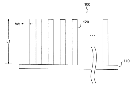
(0048] Fig. I is a side view of a percutaneous electrode array;
[0049] Fig. 2 is a cross-sectional view ofhuman skin;
CA 02529015 2005-12-09
WO 2005/002662 PCT/US2004/011395
,H, ~,Q,O~,p];, , ~ ,~,; t... f~', g. ,3"~s ~,~~~!iew of a percutaneous
electrode array comprising an
f ..,. ~~ .~~~ !r...f . .r ~,.,1 ~i , w . .~~. ~f~~ ~I ..:;n
adhesion layer;
[0051] Fig. 3A is an exemplary embodiment of a percutaneous electrode array
comprising a substrate with voids and an adhesion layer;
[0052] Fig. 3B is a top view of a percutaneous electrode array for use with an
adhesion layer;
[0053] Fig. 3C is a mechanical drawing illustrating an exemplary embodiment of
a
percutaneous electrode array substrate and electrodes;
[0054] Fig. 4 is a side view of an electrode substrate and an adhesion layer
having
an integrated capacitive element;
[0055] Fig. 5 is an exemplary circuit for measuring the capacitance of the
capacitive
element;
[0056] Fig. 6 is a side view of an electrode comprising an integrated thermal-
sensing
element;
(0057] Fig. 6A is a circuit diagram of an exemplary circuit that measures the
temperature of an integrated thermistor;
[0058] Fig. 6B is a circuit diagram of an exemplary circuit that measures the
temperature of an integrated semiconductor junction;
(0059] Fig. 6C is a circuit diagram of an exemplary circuit that measures the
temperature of a thermocouple.
DETAILED DESCRIPTION OF THE INVENTION
[0060] The preferred embodiment disclosed provides for the application of
therapeutic electrical signals to the body through a percutaneous electrode
array. The array
efficiently delivers therapeutic electrical energy into the body provided by
an electro-
therapy generator device. An electro-therapy generator device suitable for the
production of
such energy is described in U.S. patent application No. 09!756,999, entitled
"Electro-
Therapy Method and Apparatus," filed on January 8, 2001 (and identified by
Pennie &
Edmonds attorney docket no. 9756-005-999), which is hereby incorporated by
reference in
its entirety for each of its teachings and embodiments.
(0061] The configuration of a percutaneous electrode array is shown in Fig. 1.
As
shown in Fig. l, the array comprises a substrate 110 and a plurality of
electrodes I20.
Electrodes 120 are attached to a top side of substrate 1 I0. An electrical
connection to the
array is made an the bottom side of substrate 1 I O and preferably the entire
bottom surface
_g_
CA 02529015 2005-12-09
WO 2005/002662 PCT/US2004/011395
,fit ~ a ar~,ay.i~,.,~r~te,,cl,~c~,i~ i~l~."~.~znsulating material, for
example a woven plastic or fabric
a= ~ ;;
cover.
[0062] Preferably, each electrode 120 comprises a rectangular parallelepiped
attached at a proximal end to the substrate. Alternatively, each electrode 120
preferably
comprises a cylinder or cone. The distal end of either electrode embodiment
preferably
further comprises one or more of a rounded triangular and pointed tip. The
width or
diameter W1 of each electrode is preferably between 20 to 250 micrometers.
[0063] The total surface area of the electrodes in the array equals the area
of each
electrode times the number of electrodes in contact with the skin. This area
must be Large
enough to carry the electrical current introduced into the body by the electro-
therapy
generator device,. while limiting the current density through the attached
skin area. The
surface area of each electrode comprises the area of the distal tip of the
electrode plus the
surface area along the effective length of the electrode, L1, i.e. the length
that is inserted
into the skin. Preferably, the total electrode surface area is greater than
0.2 square
centimeters.
[0064] In an alternate preferred embodiment, the total electrode surface area
is Less
than 0.2 square centimeters, but the substrate has a surface area greater than
14.1 square
millimeters. The current conducting area of the substrate in combination with
the area of
the electrodes limits the current density to the skin.
[0065] The effective contact area of the electrodes is equal to the total
surface area
of the electrodes times a 56% reduction factor that accounts for the electrode
element
surface area which comes in contact with the body's ionic environment
(70°!° of the
electrode's length), and the number of electrodes that are in contact with the
skin (80% of
the total number of electrodes in the array). The Food and Drug Administration
(FDA)
currently limits the current density for electro-therapy devices to less than
10 milliamps per
square centimeter of contact area. One with skill in the art will recognize
that several
different configurations can be employed in order to achieve the necessary
effective contact
area needed to reduce the current density below the FDA limit. One way to
increase the
area is to increase the length Ll of each electrode 120 in the percutaneous
electrode array,
i.e., the length in contact with the ionic environment of the body, in order
to maximize the
area for electrical conduction. The maximum length is determined by observing
the
structure of the skin in the human body.
[0066] Fig. 2 illustrates a typical cross section of skin. The top layer of
skin
disclosed in Fig. 2, the stratum corneum, is comprised mostly of dead skin
cells. Other
layers beneath the stratum corneum include the stratum lucidum, stratum
granulosum,
_g_
CA 02529015 2005-12-09
WO 2005/002662 PCT/US2004/011395
~~.~.s,~ra rrk ino ~,axsc~kth~ ;s.~,,ra~ basale. These five layers are
collectively known as the
,E",~
epidermis. The epidermis covers the germinating skin layers, known as the
dermis, which
also contains nerves, arteries, veins, or lymphatic vessels. Depending on the
location of the
skin and its condition, the thickness of the epidermis is approximately 120 to
500 um. The
effective length of electrodes 120 is preferably between 120 and S00 um, and
more
preferably between 150 and 200 um so that the tip of electrode I20 penetrates
into the
epidermis, but does not reach any nerves, arteries, veins, or lymphatic
vessels. The
effective length of the electrodes is preferably adapted to the location where
the array is
attached and to the condition of the skin within that region of body. The
electrode length is
tailored to match these variables, enabling the electrode array to
successfully transit to a
point just past the epidermis. This region is mostly devoid of pain receptors,
making the
insertion of the percutaneous electrode array virtually painless. The elastic
properties of the
skin helps seal holes le$ behind by electrodes 120 after the array has been
removed.
Furthermore, the small diameter of each electrode 120, about the diameter of a
typical
human hair, will limit the amount of fluid that could flow through the hole
created by the
electrode.
.[0067] " The major axes of electrodes 120 are preferably perpendicular to
substrate
I 10, but may be angled between perpendicular and parallel to the substrate.
Altering the
mechanical properties of substrate 1 IO andlor electrodes 120 may enhance
adhesion of the
array to the skin. The electrical contact integrity can be impro-ved or
maintained by
increasing.the tension along the plane of substrate 110 between electrodes 124
and the skin
surrounding the region of penetration. For example, substrate 110 may act as a
spring. In
this example, array 100 would be flexed prior to insertion. When array 100 is
released, the
tension stored in substrate 110 would force electrodes 120 against the skin.
[0068] In an alternative preferred embodiment, array 100 comprises a shape-
memory metal, e.g., Nitinol. The transition temperature of the alloy is
preferably correlated
with skin temperature by formulation and processing of the alloy. An array 100
made from
such materials would preferably expand or contract along a designated axis
along the
surface area of substrate I 10. The expansion or contraction would force
electrodes 120
laterally against the skin.
[0069] Electrodes 120 are preferably composed of material having good
electrical
conductive properties, such as doped silicon, silicon-metal compounds,
nickel/iron alloy,
stainless steel, conductive inks, an allotrope of carbon such as glassy carbon
derived from
high carbon content polymer pyrolysis, conductive polymers, polymerlgraphite
or
polymer/metal composite blends, and other biocompatible metals. The materials
also have
-10-
CA 02529015 2005-12-09
WO 2005/002662 PCT/US2004/011395
~s~,fli. ep~t~ ear s en~gt ~ ~~!~nt the fracture of electrodes in the skin. In
the preferred
a!~='" .t " 'cry ", .~,~;".n n";I. ~j« ,.. ".~'' ,~1° ;,."L.r~ ";.. ~
",;,a
embodiment, the array comprises type 316 stainless steel.
[0070] As demonstrated above, the dimensions of the percutaneous electrode
array
are extremely small. The development of such small stnzctures are known in the
art as
micro electrical mechanical systems, or MEMS. MEMS is a multidisciplinary
field
encompassing microelectronic fabrication, polymerization techniques, physical
chemistry,
life sciences and mechanical engineering. This cross-field environment has led
to the
development of micro and nano-sized structures such as micro-sensors, micro-
motors and
blood chemistry systems-on-a-chip. The manufacture of some percutaneous
electrode array
embodiments may draw on knowledge from this field, as discussed below.
[0071] In an alternative preferred embodiment, glassy carbon electrodes can be
made from any high carbon content polymer, such as pitch and
polyacrylanitrile. The
material is formed into the micro-eletromechanical structures described above
using the
LIGA process. LIGA is a micromachining technology in which X-ray radiation is
used in
the production of high-aspect ratio, precision microstructures. LIGA parts are
typically 2D
extruded metal shapes, but 3D structures can be created using this process. In
the process,
a master meld is created from silicon using semiconductor lithographic
processing. This .
mold is used to make replica molds by electroplating thin film silver followed
by nickel.
The replica maid has a thickness of 0.3 mm or greater depending on the
mechanical loads
bozne by it. Next, polymeric material is heated and softened and rolled into a
film. . The .
film is placed against the replica. Pressure is applied to force the polymeric
material into
the mold. After a short time period, the temperature is reduced and the
pressure removed.
[0072] Once the piece is formed, it is fired at 400 C to drive off volatile
chemicals
and to thermoset the plastic. This is followed by an 800 C bake in inert
atmosphere to form
carbonized material. The piece is further baked at about 1100 C to increase
conductivity by
forming a graphitic phase. Due to the small size of the electrodes, the
relatively low strain
properties of the material do not present a breakage problem, even after many
insertion
cycles.
[0073] In an alternative preferred embodiment, conductive inks are sprayed
onto the
electrode array formed from a polymer such as polymethyl methacrylate, or
PMMA.
Moderate heating to about 120 C increases both the conductivity and adhesion
of the
conductive film.
[0074] In another alternative preferred embodiment, indium tin oxide is
applied to a
PMMA electrode array. A glycol-metal precursor of indium tin oxide is sprayed
ar spin-
-I1-
CA 02529015 2005-12-09
WO 2005/002662 PCT/US2004/011395
~,cr~rat~d;o~tcc~:;;~:c~ ~,r~y,;~.n~l ~t~~~, ~,~ated to about 400C to form a
conductive film coating.
u...;
~ ~...~. n ., a ", ~ , , ~" .",, i "., t
Indium tin oxide coatings exhibit superb conductivity properties.
[0075] In another alternative preferred embodiment, a polymer blend is used to
form
the array. In such an array, a Iarge amount of either metal powder or graphite
powder or
graphite-nanofiber is added to a plastic precursor to render the final
material moderately
conductive. Aggregation of high concentrations of the conductive material can
lead to poor
uniformity in the surface conductivity of the final composite device. Thermal
processing of
the composite, where some of the volatile components of the mixture are driven
off, may
help to reduce this deleterious effect.
[0076] In another alternative preferred embodiment, pure metal is
electrodeposited
on a master mold defining the electrode structure. Preferably, the metal has a
conductivity
between 100 and 10000 S/cm.
[0077] In an alternate embodiment, an adhesion layer is added to the array to
increase the conductivity of the array and adhere the array to the skin. Fig.
3 illustrates a
percutaneous electrode arrays that includes an adhesion layer. Array 304
comprises a
substrate 3.10, a plurality of electrodes 320, and an adhesion layer 330. In a
preferred
method of manufacture, adhesion layer 330 is added to percutaneous electrode
array 300 by
depositing:material to form the layer on the surface of substrate 310 between
electrodes 320,
or by piercing a sheet of layer material with array 300. Other methods may be
evident to
one with skill in the art.
[0078] Figs. 3A-3C illustrate a preferred embodiment of a percutaneous
electrode
array that includes an adhesion layer. More specifically, array 300
illustrated in Fig. 3A
comprises a substrate 310, a plurality of electrodes 320, an adhesion layer
330, and a
plurality of voids 340 in substrate 310. Adhesion layer 330 is mounted to a
rear side of
substrate 3 z 0 and protrudes through voids 340 in substrate 310. Adhesion
layer 330 secures
the electrode to the patient, and preferably aids in the conduction of the
electrical signal into
the body. Substrate 310 provides support for adhesion layer 330.
[0079] Fig. 3B depicts a top view of array 300 before application of adhesion
layer
330. Electrodes 320 and voids 340 are airanged in a grid pattern. Preferably,
array 300 is
manufactured from a sheet of stainless steel stamped and/or etched to produce
voids 340
and electrodes 320 within the area of voids 340. Electrodes 320 are bended
upward so that
the major axis is in the desired direction, preferably normal to the surface
of substrate 310.
[0080] Fig. 3C is a mechanical drawing depicting an exemplary embodiment of
percutaneous electrode array 300. The array comprises 3600 electrodes arranged
in a
regular grid pattern of 60 by 60. The width W 1 of each electrode is
approximately 200 um.
-12-
CA 02529015 2005-12-09
WO 2005/002662 PCT/US2004/011395
..di tams ,~ l bou 8 0 ; a arates the electrodes. These dimensions result in a
5 cm
". ~".v,""i~ ~:~~"~,; ",~" ",~ ",;;f~''~.,°,'E ,~;ap
E,",
by 5 cm array of electrodes. Detail A shows the electrodes within the void
area before they
are bent upwards.
[0081] Suitable materials for use in layer 330 axe a hydrogel or sol-gel
construct
containing an electrolyte. The minimum height of the hydrogel layer, H1, is
limited by the
estimated evaporation time and the mechanical modulus of the gel. In a
preferred
embodiment, the array comprises a 635 um thick conductive gel, e.g. Uni-Patch
type
RG63B. As the hydrogel is exposed to the air, the water in the gel will
evaporate, drying
out the array and reducing the adhesive and conductive properties of the gel.
The use of
such an array would require a higher applied voltage. If the array is flexed
or the skin/array
mechanical interface is otherwise altered, an instantaneous drop in
interfacial impedance
can occur, giving rise to an unpleasant feeling in the patient and
concentrating the current at
points of good contact, raising the possibility of a,thermal burn. Adhesion
layer 330 is
preferably adapted to provide an indication that the array is no longer
suitable for use.
[0082] In a preferred embodiment, the hydrogel contains materials well known
in
the art that, when exposed to air after the packaging material containing the
electrode is
opened, causes the hydrogel to slowly change color as a function of the
evaporation rate.
For example, the hydrogel may have a normally clear appearance, but would turn
into a
dark color after exposure to the atmosphere. Alternatively, the:normal
appearance of the
hydrogel may be colored, and after exposure the hydrogel turns clear. Such
color changes
indicate that the array needs to be replaced or that the integrity of the
packaging is
compromised and that the array is no longer sterile. In an alternate preferred
embodiment,
after the hydrogel has come into direct contact with human skin, a chemical
reaction would
occur which changes the color of the hydrogel without leaving any residue on
the skin.
[0083] In an alternative preferred embodiment, an adhesion layer of an
electrode is
monitored to determine if the array has dried out or if the temperature is
increasing by
measuring the electrical capacitance of the adhesion layer. Fig. 4 discloses
the components
of this embodiment. As shown in Fig. 4, the electrode comprises a substrate
4L0, an
adhesion layer 430 and a capacitive plate. 440 covered by an insulating Layer
450.
Capacitive plate 440 comprises a small section of conductive material on the
bottom side of
adhesion layer 430, thus forming an electrical capacitor comprising a
dielectric (adhesion
layer 430} between two conductive plates (substrate 410 and plate 440). The
capacitance of
the array capacitor is a function of both temperature and moisture content. An
electrical
lead is connected to plate 440 for connection in a monitoring circuit.
Insulating layer 450 is
coated over plate 440 to prevent plate 440 from elec'cally contacting the
patient or others.
-I3-
CA 02529015 2005-12-09
WO 2005/002662 PCT/US2004/011395
,QQ, .4j ~~,;, ,. ~i'wcu~~s"~h,~,~~ ~e~4~,~ure capacitance are well known in
the art. An exemplary
°~" ~,.". ~ "~ " ~~",I1.,~;is it"1~ ~ ~~II ",° ~ ~ , :xu
circuit for measuring the array capacitance is illustrated in Fig. 5.
Measuring system 500
comprises a pair of identical low-pass filters 510, 520, a pair of low-offset
comparators 530,
540, a flip-flop 550, a binary counter 560, a microcontroller 570 and a high
frequency clock
580. A stable sinusoidal signal, a component of the signal generated by the
electro-therapy
generator device described in more detail in U.S. patent application No.
091756,999, entitled
"Electro-Therapy Method and Apparatus," filed on 3anuary 8, 2001 (and
identified by
Pennie & Edmonds attorney docket no. 9756-005-999), is used to determine the
capacitance
of adhesion layer 430.
[0085j Substrate 410 and capacitive plate 440 are connected to a monitoring
circuit
comprising low-pass filters 510, 520. Filters 510, 520 preferably comprise 8-
pole switched
capacitor filters that pass a stable sinusoidal signal. Cornparators 530, 540,
detect the zero
crossings of the stable sinusoidal output applied to the reference, a fixed
precision resistor,
and the array capacitor. Reference comparator 530 sets flip-flop 550, which
starts counter
560, and capacitance comparator 540 resets flip-flop 550, which stops counter
560. High
frequency clock 580 provides a..clocking signal to counter 560 which
increments the counter
once it is started. Counter 560 counts until the capacitance signal performs
its zero
crossing. Microcontroller 570 reads the count and then resets counter 560.
Thus, counter
560 measures the time difference between the zero crossings of the reference
signal and the
current through the capacitor. Microcontroller 570 determines the phase. shift
between the
signals from the count, which is indicative of the capacitance of the array
capacitor. This
measurement is independent of the amplitude of the two signals.
Microcontroller 570
comprises embedded software that uses this information to determine if the
change in
capacitance represents a fault state. If such a determination is made, it can
shut the system
down and inform the user of the error condition. The software requires that a
specific
profile of the change in capacitance be maintained during system operation.
[0086] Fig. 6 discloses a preferred embodiment of an electrode comprising a
substrate 610 and a temperature-sensing element 640 bonded to substrate 610.
The element
comprises one of a thermistor, a diode, or other semiconductor junction, and a
thermocouple. Irt a preferred embodiment, temperature element 640 is a small
device,
typically no more than 0.5 mm in thickness. Temperature element 640 accurately
measures
the temperature of substrate 610.
[0087j In an alternative preferred embodiment, an electrode comprising an
adhesion
layer has temperature-sensing element 640 embedded in the adhesion layer to
monitor the
integrity of the adhesion Layer, for reasons stated above in the capacitance
embodiment.
-14-
CA 02529015 2005-12-09
WO 2005/002662 PCT/US2004/011395
.t[OQ, ,8] ., F~ . ,6,A i ~"~ x ~t dia am of an exem 1 circuit that measures
the
u,~v ~"., ~ .._ °.' kE",i# ;'.;;:i~ i~:"Ik ~,~°~,: ~ ."fl~.
.,.(f.. .,.,:I~'~;;I~r;; v ~ p ~'Y
temperature of a percutaneous electrode array comprising an integrated
thermistor. In this
embodiment, thermistor element 640 is connected to a monitoring circuit
comprising a
voltage divider bridge circuit 650, a differential amplifier 660, an analog-to-
digital
converter 670 and a microcontroller 680. Amplifier 660 eliminates any common
mode
noise associated with the Iead length from the element 640 to the monitoring
circuit. The
resultant voltage from amplifier 660 varies as a function of array
temperature. The
monitoring circuit converts the voltage signal to a binary value by analog-to-
digital
converter 6?0. The monitoring circuit further comprises microcontroller 680
having
software that converts the binary representation of the voltage signal into
the temperature of
the array.
[0089] Fig. 6B is a circuit diagram of an exemplary circuit that measures the
temperature of a percutaneous electrode array comprising either an integrated
semiconductor or discrete-device semiconductor junction. In this embodiment,
element 640
comprises a diode or transistor having a well-characterized, temperature
dependent behavior
that measures temperature to a high precision. As shown in Fig. 6B, the
junction is
connected to a monitoring circuit comprising a constant current source 651, a
reference
resistor 652, an amplifier 660, an analog-to-digital converter 670, and a
microcontroller
680. The current is supplied to junction' 640 through resistor 652 to forward
bias junction
640. A voltage is measured across junction 640, which varies with junction
temperature.
The relationship between the junction voltage and temperature is:
[00901 Vjunction = kT/q * In(Ijunction/Ijunction saturation current), where lc
is
Boltzmann's constant (1.38 x. lO-23 3/K), T is the absolute temperature in
degrees Kelvin, q
is the electron charge (1.601 x 10⁻¹⁹ coulomb), Ijunction is the constant
supplied reference
current, and Ijunction saturation current is the saturation current of the
semiconductor
device (2 x Z 0'I6 A for silicon).
[0091] Amplifier 660 increases the junction voltage to a useful level and
converter
670 transforms the signal into a binary representation. Microcontroller 680
uses the binary
representation to determine the array temperature.
[0092 Fig. 6C is a circuit diagram of an exemplary circuit that measures the
temperature of a percutaneous electrode array comprising a thermocouple. In
this
embodiment, temperature element 640 comprises a thermocouple. A thermocouple
is a
device comprising two dissimilar metals (e.g., platinum and rhodium) in
electrical contact
with each other at a junction. The device generates an electromotive force
correlated to the
temperature at the junction. The thermocouple requires compensation for the
temperature
-15-
CA 02529015 2005-12-09
WO 2005/002662 PCT/US2004/011395
~tf. a j~~ ~xi,pp~, fo~,a b, ,tw. ,.~~~u the device and its connecting leads
(cold junction
~t"~' ~,.,~. . ~ ,.,.U if,.,lr ~.,lf..,;~, .~.. ,.:~ ~I,;~~C',',;;:lj
compensation).
[0093] The monitoring circuit illustrated in Fig. 6C comprises an amplifier
660, a
analog-to-digital converter 670 and a microcontroller. Amplifier 660 amplifies
thermocouple 640's output voltage, converter 670 converts it to a binary
representation, and
then software in microcontroller 680 uses the binary voltage value to
determine the array's
temperature. Amplifier 660 contains the necessary components to effect cold
junction
compensation circuitry as is well known in the art. The software contains a
lookup table as
is well known in the art to convert the binary representation of thermocouple
voltage to
temperature.
[0094] In a preferred embodiment, the measured temperature paxaxneter is used
as
an interlock in the electro-therapy generator device to protect the patient
from harm. If for
some reason the array rises above 40 degrees Celsius, or ramps up in
temperature at a higher
rate than would normally be expected, a temperature-monitoring portion of the
electro-
therapy generator device can interrupt its output, thus lessening or
eliminating the
possibility of a burn or thermal irritation. Such detected conditions are used
to inform the
.operator of potential problems with the integrity of the percutaneous
electrode array, or the
adhesion or placement of the array, two of the mast likely causes of an
increase in current
density. ,
[0095] In. another embodiment, the electro-therapy generating device
continuously
monitors the impedance of the percutaneous electrode array. The device
includes a warning
indicator which alerts the operator when the impedance of the percutaneous
electrode array
is too high, indicating that the array sho~xld be checked or replaced. The
indicator would
provide one or more of a visual indication, for example a blinking light
emitting diode
(LED) or an error message on an liquid crystal display (LCD), an audio
indication 'such as a
beeping sound, and a sensory indication such as a vibration producing device.
The warning
indicator can also be used to indicate error conditions such as a loose array,
unplugged lead
wires, weak batteries, missing temperature signal, missing capacitance
monitoring signal, or
any other defective condition of the array.
[0096] While the invention has been described with reference to preferred
embodiments, it will be understood by those skilled in the art that various
changes may be
made and equivalents may be substituted fox elements thereof without departing
from the
scope of the invention. In addition, many modifications may be made to adapt a
particular
situation or material to the teachings of the invention without departing from
the essential
scope thereof Therefore, it is intended that the invention not be limited to
the particular
-16-
CA 02529015 2005-12-09
WO 2005/002662 PCT/US2004/011395
a bo
,FjfE E~, ", ,~irr~ ~~~~ ~lo$e a bg,~t mode contemplated for this invention,
but that the
~.,..
.._~ ~e~ ;:.:a~ ~~t~~f~~ "~ .:;~ ~ huh .,... ~
invention will include all embodiments falling within the scope of the
appended claims.
-17-