Note: Descriptions are shown in the official language in which they were submitted.
CA 02529047 2005-12-07
Attorney Docket No. OS-1-205
FIXED PHASE POWER CONTROLLER
WITH ANALOG TRIGGER
Background of the Invention
[0001] The present invention is directed to a power controller that supplies a
specified power to a load, and more particularly to a voltage converter for a
lamp that
converts line voltage to a voltage suitable for lamp operation.
[0002] Some loads, such as lamps, operate at a voltage lower than a line (or
mains) voltage of, for example, 120V or 220V, and for such loads a voltage
converter
that converts line voltage to a lower operating voltage must be provided. The
power
supplied to the load may be controlled with a phase-control power circuit that
includes an
RC circuit. Some loads, such as lamps, operate most efficiently when the power
is
constant (or substantially so). However, line voltage variations are magnified
by phase-
control power circuits due to their inherent properties, thereby decreasing
the stability of
the power supplied to the load.
[0003] A simple four-component RC phase-control clipping circuit demonstrates
a problem of conventional phase-control clipping circuits. The phase-
controlled clipping
circuit shown in Figure 1 has a capacitor 22, a diac 24, a triac 26 that is
triggered by the
diac 24, and resistor 28. The resistor 28 may be a potentiometer that sets a
resistance in
the circuit to control a phase at which the triac 26 fires.
CA 02529047 2005-12-07
[0004] In operation, a clipping circuit such as shown in Figure 1 has two
states.
In the first state the diac 24 and triac 26 operate in the cutoff region where
virtually no
current flows. Since the diac and triac function as open circuits in this
state, the result is
an RC series network. Due to the nature of such an RC series network, the
voltage across
the capacitor 22 leads the line voltage by a phase angle that is determined by
the
resistance and capacitance in the RC series network. The magnitude of the
capacitor
voltage V~ is also dependent on these values.
[0005] The voltage across the diac 24 is analogous to the voltage drop across
the
capacitor 22 and thus the diac will fire once breakover voltage VBO is
achieved across the
capacitor. The triac 26 fires when the diac 24 fires. Once the diac has
triggered the triac,
the triac will continue to operate in saturation until the diac voltage
approaches zero.
That is, the triac will continue to conduct until the line voltage nears zero
crossing. The
virtual short circuit provided by the triac becomes the second state of the
clipping circuit.
[0006] Triggering of the triac 26 in the clipping circuit is forward phase-
controlled by the RC series network and the leading portion of the line
voltage waveform
is clipped until triggering occurs as illustrated in Figure 2. A load attached
to the
clipping circuit experiences this clipping in both voltage and current due to
the relatively
large resistance in the clipping circuit.
[0007] Accordingly, the RMS load voltage and current are determined by the
resistance and capacitance values in the clipping circuit since the phase at
which the
clipping occurs is determined by the RC series network and since the RMS
voltage and
current depend on how much energy is removed by the clipping.
CA 02529047 2005-12-07
[0008] With reference to Figure 3, clipping is characterized by a conduction
angle
a and a delay angle 8. The conduction angle is the phase between the point on
the load
voltage/current waveforms where the triac begins conducting and the point on
the load
voltage/current waveform where the triac stops conducting. Conversely, the
delay angle
is the phase delay between the leading line voltage zero crossing and the
point where the
triac begins conducting.
[0009] Define V;rrms as RMS line voltage, Vo«"S as RMS load voltage, T as
period,
and ~ as angular frequency (rad) with co = 2~f.
[0010] Line voltage may vary from location to location up to about 10% and
this
variation can cause a harmful variation in RMS load voltage in the load (e.g.,
a lamp).
For example, if line voltage were above the standard for which the voltage
conversion
circuit was designed, the triac 26 may trigger early thereby increasing RMS
load voltage.
In a halogen incandescent lamp, it is particularly desirable to have an RMS
load voltage
that is nearly constant.
[0011] Changes in the line voltage are exaggerated at the load due to a
variable
conduction angle, and conduction angle is dependent on the rate at which the
capacitor
voltage reaches the breakover voltage of the diac. For fixed values of
frequency,
resistance and capacitance, the capacitor voltage phase angle (6C) is a
constant defined by
6~ = arctan (-ARC). Therefore, the phase of Vo is independent of the line
voltage
magnitude. However, the rate at which V~ reaches Vao is a function of V;rr",s
and is not
independent of the line voltage magnitude.
[0012] Figure 4 depicts two possible sets of line voltage V; and capacitor
voltage
V~. As may be seen therein, the rate at which V~ reaches VBO varies depending
on V;~«"S.
CA 02529047 2005-12-07
For RC phase-control clipping circuits the point at which V~ = VBO is of
concern because
this is the point at which diac/triac triggering occurs. As V;~rms increases,
V~ reaches VBo
earlier in the cycle leading to an increase in conduction angle (a2 > a; ),
and as V;rrms
decreases, V~ reaches VBO later in the cycle leading to a decrease in
conduction angle (a2
a,).
[0013] Changes in V;rrms leading to exaggerated or disproportional changes in
Vorrn,s are a direct result of the relationship between conduction angle and
line voltage
magnitude. As V;~",S increases, Vornns increases due to both the increase in
peak voltage
and the increase in conduction angle, and as V;~r",S decreases, V~rrms
decreases due to both
the decrease in peak voltage and the decrease in conduction angle. Thus, load
voltage is
influenced twice, once by a change in peak voltage and once by a change in
conduction
angle, resulting in unstable RMS load voltage conversion for the simple phase-
control
clipping circuit.
[0014] When a voltage converter is used in a lamp, the voltage converter may
be
provided in a fixture to which the lamp is connected or within the lamp
itself. U.S. Patent
3,869,631 is an example of the latter, in which a diode is provided in an
extended stem
between the lamp screw base and stem press of the lamp for clipping the line
voltage to
reduce RMS load voltage at the light emitting element. U.S. Patent 6,445,133
is another
example of the latter, in which a voltage conversion circuit for reducing the
load voltage
at the light emitting element is divided with a high temperature-tolerant part
in the lamp
base and a high temperature-intolerant part in a lower temperature part of the
lamp
spaced from the high temperature-tolerant part.
4
CA 02529047 2005-12-07
[0015] Factors to be considered when designing a voltage converter that is to
be
located within a lamp include the sizes of the lamp and voltage converter,
costs of
materials and production, production of a potentially harmful DC load on a
source of
power for installations of multiple lamps, and the operating temperature of
the lamp and
an effect of the operating temperature on a structure and operation of the
voltage
converter.
Summary of the Invention
[0016] An object of the present invention is to provide a novel fixed phase
power
controller that converts a line voltage to an RMS load voltage using an analog
trigger.
[0017] A further object is to provide a fixed phase power controller and
method in
which an analog device, such as a capacitor, receives an input that is
independent of a
change in magnitude of a line voltage and charges and discharges to provide an
analog
trigger signal at a first frequency that defines the RMS load voltage, in
which a reset
circuit periodically resets an initial condition of the analog device, in
which a sync signal
synchronizes the trigger signal with a waveform of the line voltage, and in
which a
control circuit clips a load voltage based on the analog trigger signal to
define the RMS
load voltage.
[0018] A yet further object is to provide a lamp with this fixed phase power
controller in a voltage conversion circuit that converts a line voltage at a
lamp terminal to
the RMS load voltage usable by a light emitting element of the lamp.
CA 02529047 2005-12-07
Brief Description of the Drawings
[0019] Figure 1 is a schematic circuit diagram of a phase-controlled dimming
circuit of the prior art.
[0020] Figure 2 is a graph illustrating voltage clipping in the phase-
controlled
dimming circuit of Figure 1.
[0021] Figure 3 is a graph showing the conduction angle convention adopted
herein.
[0022] Figure 4 is a graph showing how capacitor voltage affects conduction
angle.
[0023] Figure 5 is a partial cross section of an embodiment of a lamp of the
present invention.
[0024] Figure 6 is a schematic circuit diagram of a fixed phase power
controller
illustrating an embodiment of the present invention.
[0025] Figure 7 is a schematic circuit diagram of an embodiment of the analog
control block of Figure 6.
(0026] Figure 8 is a schematic circuit diagram of an embodiment of the reset
circuit of Figure 6.
[0027] Figure 9 is a schematic circuit diagram of an embodiment of the
transistor
switch of Figure 6.
[0028] Figure 10 is a graph showing the relationship between output voltage
(VoRMS) and input voltage (ViRMS) for a prior art RC phase-controlled clipping
circuit
designed to produce 42VRMS output (load voltage) for 120VRMS input (line
voltage).
6
CA 02529047 2005-12-07
[0029] Figure 11 is a graph showing the relationship between output voltage
(VoRMS) and input voltage (V~RMS) for a fixed phase power controller of the
present
invention designed to produce 42VRMS output (load voltage) for 120VRMS input
(line
voltage).
Description of Preferred Embodiments
[0030] With reference now to Figure 5, a lamp 10 includes a base 12 with a
lamp
terminal 14 that is adapted to be connected to line (mains) voltage, a light-
transmitting
envelope 16 attached to the base 12 and housing a light emitting element 18
(an
incandescent filament in the embodiment of Figure 5), and a fixed phase power
controller
20 for converting a line voltage at the lamp terminal 14 to a lower operating
voltage. The
power controller 20 is within the base 12 and connected between the lamp
terminal 14
and the light emitting element 18. The power controller 20 may be an
integrated circuit
in a suitable package as shown schematically in Figure 1. Preferably, the
power
controller 20 is entirely within the base as shown in Figure 5.
[0031] While Figure 5 shows the power controller 20 in a parabolic aluminized
reflector (PAR) halogen lamp, the power controller 20 may be used in any
incandescent
lamp when placed in series between the light emitting element (e.g., filament)
and a
connection (e.g., lamp terminal) to a line voltage. Further, the power
controller described
and claimed herein finds application other than in lamps and is not limited to
lamps.
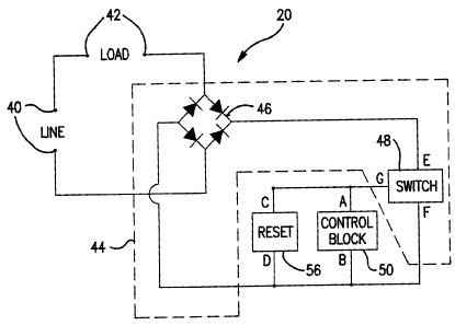
[0032] With reference to Figure 6, an embodiment of the fixed phase power
controller 20 of the present invention converts a line voltage at line
terminals 40 to an
RMS load voltage at load terminals 42. The power controller 20 includes a
control
CA 02529047 2005-12-07
circuit 44 that includes a full wave bridge 46 that is connected to the line
and load
terminals and a transistor switch 48 that is connected to the bridge 46 and
that turns on
and off to clip the load voltage to provide the desired RMS load voltage. As
explained
below, the clipping is carried out with a constant conduction angle that is
independent of
changes in the line voltage so that the phase of the circuit is fixed to
provide a stable
RMS load voltage even when the line voltage changes.
[0033] The power controller 20 also includes an analog control block 50 that
triggers conduction of the transistor switch 48 at the appropriate frequency
to define the
RMS load voltage. The analog control block 50 receives an input that is
independent of a
change in magnitude of the line voltage and charges and discharges to provide
a trigger
signal at a first frequency that turns the transistor switch off and on so as
to achieve the
desired RMS load voltage.
[0034] In a preferred embodiment and with reference to Figure 7, the analog
control block 50 includes a capacitor 52 that receives a DC signal from a DC
source 54
that is independent of the line voltage. The capacitor 52 receives the DC
signal and is
charged at a known rate based on its time constant and will discharge at a
determinable
level to provide the trigger signal to the transistor switch at a determinable
frequency.
Therefore, the timing to reach the triggering level can be hard-wired into the
circuit to set
the conduction angle of the fixed phase power controller. The capacitor may be
replaced
with an equivalent component or circuit that receives the DC signal and
charges and
discharges to provide the trigger signal at the first frequency.
[0035] The preferred embodiment also includes a reset circuit 56 that resets
the
initial condition of the analog control block 50 each half cycle to ensure
consistent
CA 02529047 2005-12-07
triggering during operation. As seen in Figure 8, the reset circuit preferably
includes
opposed diodes 58 (one of which may be a semiconductor controlled rectifier -
SCR) that
are connected in parallel with the analog control block 50. The opposed diodes
may be
replaced with an equivalent component or circuit that resets the initial
condition of the
analog control block.
[0036] The power controller preferably operates with the charging and
discharging of the analog control block synchronized with the waveform of the
line
voltage. That is, in order for the conduction angle to be constant, the
clipping should
occur at the same place on the waveform each cycle. This is achieved by
synchronizing
the trigger signals with the waveform of the line voltage either at the analog
control block
50 or the reset circuit 56. The embodiments shown in Figures 7-8 both include
the
synchronization connections that provide a sync signal, although such
connections may
be found in one of these.
[0037] The transistor switch 48 can take various forms and may, for example,
be
an SCR, a triac, a diac or a diac in combination with an SCR or triac. Figure
9 illustrates
a diac 60 that turns on and off an SCR 62 in response to the trigger signal
from the analog
control block. Other equivalent transistor switches are known and usable
herein (such as
described in the above-noted applications), and need not be explained to those
of skill in
the art.
[0038] In operation, the fixed phase clipping of the present invention
provides a
solution to the problem of conventional RC phase-controlled clipping. The
solution is
similar to the conventional scheme except that the conduction angle is
independent of
other circuit variables. Figures 10 and 11 illustrate the improvement of the
present
CA 02529047 2005-12-07
invention. Figure 10 is a graph showing the relationship between output
voltage (VoRMS)
and input voltage (V,RMS) for a prior art RC phase-controlled clipping circuit
designed to
produce 42VRMS output (load voltage) for 120VRMS input (line voltage). Figure
11 is a
graph showing the relationship between output voltage (VoRMS) and input
voltage (V,RMS)
for a fixed phase power controller of the present invention designed to
produce 42VRMs
output (load voltage) for 120VRMS input (line voltage). As is apparent, the
output voltage
varies considerably less in a device of the present invention than in the
comparable prior
art device.
[0039] The description above refers to use of the present invention in a lamp.
The
invention is not limited to lamp applications, and may be used more generally
where
resistive or inductive loads (e.g., motor control) are present to convert an
unregulated AC
line or mains voltage at a particular frequency or in a particular frequency
range to a
regulated RMS load voltage of specified value.
[0040] While embodiments of the present invention have been described in the
foregoing specification and drawings, it is to be understood that the present
invention is
defined by the following claims when read in light of the specification and
drawings.