Note: Descriptions are shown in the official language in which they were submitted.
CA 02529147 2005-12-09
WO 2005/001753 PCT/US2004/019917
-1-
ACQUISITION OF HIGH RESOLUTION BIOMETRIC IMAGES
RELATED APPLICATIONS
This application claims the benefit of U.S. Provisional Application No.
60/480,008, filed on June 21, 2003, U.S. Provisional Application No.
60/519,792,
filed on November 13, 2003 and U.S. Provisional Application No. 601523,068,
filed
on November 11, 2003. This application is related to the PCT Application
entitled
"Method and Apparatus for Processing Biometric Images" filed concurrently
herewith on June 21, 2004 under the attorney docket number 3174.1012-006. The
entire teachings of the above applications are incorporated herein by
reference.
BACKGROUND OF THE INVENTION
Growing concerns regarding domestic security have created a critical need to
positively identify individuals as legitimate holders of credit cards,
driver's licenses,
passports and other forms of identification. The ideal identification process
is
reliable, fast, and relatively inexpensive. It should be based on modern high-
speed
electronic devices that can be networked to enable fast and effective sharing
of
information. It should also be compact, portable, and robust for convenient
use in a
variety of environments, including airport security stations, customs and
border
crossings, police vehicles, home and office computing and entrance control
sites of
secure buildings.
A well established method for identification is to compare a fingerprint with
a previously obtained authentic fingerprint of the individual. Fingerprints
have
traditionally been collected by rolling an inked finger on a white paper.
Since this
traditional process clearly fails to meet the criteria listed above, numerous
attempts
have been made to adapt an electronically imaged fingerprint method to address
new
security demands. These modern proposals all use, as a key component, a solid-
state
device such as a capacitive or optical sensor to capture the fingerprint image
in a
digital format. By using a new type of solid-state imager as part of a
fingerprint
CA 02529147 2005-12-09
WO 2005/001753 PCT/US2004/019917
_2_
identification apparatus a ringerprint can be collected conveniently and
rapidly, for
example, during a security check, and subsequently correlated, in near real-
time, to
previously trained digital fingerprints in an electronic data base that
resides either in
a computer at the security check point, a secure but portable or removable
storage
device, or on a remotely networked server.
A typical fingerprint comprises a pattern of ridges separated by valleys, and
a
series of pores that are located along the ridges. The ridges are usually 100
to 300
~m wide and can extend in a swirl-like pattern for several mm to one or more
cm.
These ridges are separated by valleys with a typical ridge-valley period of
approximately 250-500 urn. Pores, roughly circular in cross section, range in
diameter from about 60 ~m to 240 ~m and are aligned along the ridges and can
be
isolated or grouped into two or more abutting or near abutting pore clusters.
There
are typically more than 400 pores within a fingerprint region with a frequency
of
occurrence of about 21 pores/ cm of ridge length (see Roddy A. and Stosz J.,
Proceed. IEEE, 85, 9, 1390-1421 (1997). Almost all present-day ringerprint
identification procedures use only ridge/valley minutiae patterns. These are
simpliried and identified as a pattern of ridge/valley features such as end
points,
deltoids, bifurcations, crossover points, and islands, all together referred
to as
minutiae. Typically, a relatively large area of the fingerprint is required in
order to
obtain enough unique minutiae features, for example, at least 0.50 x 0.50
inches.
Most modern fingerprint imagers therefore use up to one full inch square or
even
larger, in order to obtain enough features to perform a useful means of
identification.
Fingerprints are compared using primarily this simplified description of the
minutiae
patterns.
Due to the more demanding resolution requirements necessary to
successfully image pores, there are no commercial devices available today that
use
pores for fingerprint identification, even though there are typically 7 to 10
ten times
as many pores as minutiae in a given fingerprint area. A typical fingerprint
image as
small as 0.1 x 0.1 inches may only contain 2-5 minutiae points, not enough to
reliably identify a unique individual. The same area, however, may typically
contain
as many as 40 to 50 pores and several thousand ridge contour details, which
along
CA 02529147 2005-12-09
WO 2005/001753 PCT/US2004/019917
-3-
with a few minutiae points can positively identify an individual reliably.
Most optical designs proposed for creating fingerprint images suffer
important limitations that reduce their usefulness in real life applications.
Many
designs are not suitable, for example, to resolve pore patterns or fine detail
of the
contour of the intersection of ridges and valleys in the fingerprint. Other
designs
produce distorted images that complicate fingerprint correlation, and still
other
designs are too bulky or delicate for convenient use in the field.
One optical design that reduces the overall size of the device uses holograms
to diffract light in a desired direction. A common limitation of such devices
is
sensitivity of the intensity of illumination of the target topological surface
to
variation in temperature with respect to angle and wavelength of the incident
light.
Accordingly, there is a need for a compact, high resolution device that
reliably operates over a broad range of temperature.
SUMMARY OF THE INVENTION
The present invention relates to an apparatus and method of acquisition of an
image of any surface topology present on skin, which, by way of example, can
be a
rolled andlor slap fingerprint, palm print, etc. and hereinafter for
convenience will be
referred to as a fingerprint.
In one embodiment, the present invention is an apparatus for fingerprint
image acquisition, comprising a waveguide, having an entrance edge and top and
bottom; a light source, configured to direct a light beam at the entrance edge
of the
waveguide; a skin contact layer, disposed at or near the top surface of the
waveguide
or bottom surface of the waveguide; a holographic optical element (HOE),
disposed
at the top or at the bottom surfaces of the waveguide, configured to diffract
the light
beam incident from the light source to the skin contact layer; a sensor array,
configured to detect light reflected from the interface between skin and the
skin
contact layer. The HOE includes a layer comprising a grating and at least one
supporting layer in contact with the said grating layer, wherein the grating
layer and
the at least one supporting layer have substantially similar coefficients of
thermal
expansion or thermo-optic coefficients or both.
CA 02529147 2005-12-09
WO 2005/001753 PCT/US2004/019917
-4-
In another embodiment, the present invention is an apparatus for image
acquisition of topological features of the surface of skin, comprising a
waveguide,
having an entrance edge and top and bottom surfaces; a light source,
configured to
direct a light beam at the entrance edge of the waveguide; a skin contact
layer,
disposed at or near the top surface or the bottom surface of the waveguide; a
holographic optical element (HOE), disposed at the top or at the bottom
surfaces of
the waveguide, configured to diffract the light beam incident from the light
source to
the skin contact layer; a sensor array, configured to detect light reflected
from the
interface between skin and the skin contact layer; and means for compensating
for
changes in the Bragg matching condition of the HOE due to changes temperature.
In one embodiment, the present invention is an apparatus for image
acquisition of topological features of the surface of skin comprising a
waveguide,
having an entrance edge and top and bottom; a light source, configured to
direct a
light beam at the entrance edge of the waveguide; a skin contact layer,
disposed at
the top or bottom surface of the waveguide; a holographic optical element
(HOE),
disposed at the top or at the bottom surfaces of the waveguide, configured to
diffract
the light beam incident from the light source at the skin contact layer; a
sensor array,
configured to detect light reflected the interface between skin and the skin
contact
layer. The HOE includes at least two co-locationally multiplexed holograms.
In one embodiment, the present invention is an apparatus for image
acquisition of topological features of the surface of skin comprising a
waveguide,
having an entrance edge and top and bottom surfaces; a light source,
configured to
direct a light beam at the entrance edge of the waveguide; a skin contact
layer,
disposed at the top or bottom surface of the waveguide; a holographic optical
element (HOE), disposed at the top or at the bottom surfaces of the waveguide,
configured to diffract the light beam incident from the light source at the
skin
contact layer; a sensor array, configured to detect light reflected from the
interface
between skin and the skin contact layer; and means for changing the wavelength
of
the light source.
In one embodiment, the present invention is an apparatus for image
acquisition of topological features of skin surface comprising a waveguide,
having
an entrance edge and top and bottom surfaces; a light source, configured to
direct a
CA 02529147 2005-12-09
WO 2005/001753 PCT/US2004/019917
-5-
light beam at the entrance edge of the waveguide; a skin contact layer,
disposed at
the top surface of the waveguide; a holographic optical element (HOE),
disposed at
the top or at the bottom surfaces of the waveguide, configured to diffract the
light
beam at the skin contact layer and having a Bragg matching condition; a sensor
array, configured to detect light reflected from the interface between skin
and the
skin contact layer, and means for compensating for changes in the Bragg
matching
condition of the HOE due to changes in temperature. The light source is a
broad
wavelength spectrum light source, the wavelengths of which can reconstruct the
HOE.
In one embodiment, the present invention is a method of acquiring an image
of the topology of the surface of skin, comprising receiving a surface of skin
by a
device for image acquisition of the topological features of the surface of
skin
wherein said device includes a holographic optical element (HOE) having a
Bragg
matching condition; directing a light beam at the HOE, thereby diffracting the
light
-15 beam; directing the diffracted 1-fight beam at the interface between skin
and the skin
contact layer, thereby reflecting the light beam; compensating for temperature-
induced changes in the Bragg matching condition of the HOE; and detecting the
reflected light, thereby acquiring the image of the topological features of
the surface
of skin by said device.
It should be understood that the example embodiments described above,
include a corresponding method or apparatus embodiments.
The device of the present invention is preferably compact, possesses a bxoad
operating temperature range and advantageously allows the acquisition of
images
that capture pore structural features and fine detail features of the contour
of the
ridge structure in addition to standard minutiae structures. We have shown
that the
use of pores combined with the use of the fine detail of the ridge contour and
the
usual minutiae significantly increases the reliability of fingerprint
comparisons, and
substantially reduces the false accept rate, as well as providing positive
identification with use of fingerprint sample areas as small as 0.1 x 0.1
inches.
Various example embodiments of the instrument used to acquire images of
biometrics are described herein. The embodiments may also include alternative
embodiments of the instrument and various embodiments of acquiring, modeling,
CA 02529147 2005-12-09
WO 2005/001753 PCT/US2004/019917
-6-
preprocessing, and processing images of biometrics acquired by the instrument,
such
as those disclosed in a related application, entitled "Method and Apparatus
for
Processing Biometric Images," Attorney Docket No. 3174.1012-006, being fled
concurrently herewith. The entire teachings of the related application are
incorporated herein by reference.
BRIEF DESCRIPTION OF THE DRAWINGS
Fig. 1 is a computer network in which a fingerprint sensor according to the
principles of the present invention is deployed;
Fig. 2 is a system hierarchical diagram of the fingerprint sensor of Fig. 1;
Fig. 3 is a schematic diagram of the fingerprint sensor of Fig. 1;
Fig. 4 is a mechanical diagram of an imager in the Bngerprint sensor of Fig.
1;
Fig. 5 is a diagram of the imager of Fig. 4 with a graph illustrating peak
intensity changes of diffracted light as a function of temperature;
Figs. 6A-6E are mechanical diagrams of alternative embodiments of the
imager in the fingerprint sensor of Fig. 1;
Fig. 7A is a mechanical diagram of another embodiment of the imager of
Fig. l including means for optically detecting temperature changes;
Figs. 7B and 7C are waveforms illustrating optical feedback in the imager of
Fig.7A;
Figs. 8A-8D are mechanical diagrams of other alternative embodiments of
the imager in the fingerprint sensor of Fig. 1;
Fig. 9 is a schematic diagram of another embodiment of the imager in the
fingerprint sensor of Fig. 1 illustrating a use of a grazing incidence
reflection
grating;
Fig. 10 is a waveform plot illustrating Bragg detuning characteristics fox an
embodiment of the fingerprint sensor of Fig. 1; and
Fig. 11 is a plot of a range of diffraction efficiency as a function of the
value
of the Bragg detuning angle of Fig. 10.
CA 02529147 2005-12-09
WO 2005/001753 PCT/US2004/019917
_7_
DETAILED DESCRIPTION OF THE INVENTION
A description of preferred embodiments of the invention for a fingerprint
biometric follows. It should be understood that the principles of the present
invention and example preferred embodiments of the methods and apparatus
described below may be applied to other biometrics, including: ear shape and
structure, facial or hand thermograms, iris or retina structure, handwriting,
fingerprints, palm prints, foot prints, toe prints, or prints of other areas
of the skin,
including haix.
FIG. 1 is a system diagram in which an embodiment of a fingerprint sensor
according to the principles of the present invention is employed. The
fingerprint
sensor 100 includes a fingerprint imager 110 and fingerprint camera 120. The
imager 110 and camera 120 may be mechanically, electrically, and optically
connected in a single "box." A finger 105 or other topological surface of skin
is
placed on the fingerprint imager 110 at a "viewable" location by the imager
110 for
acquisition of a forgerprint or information of other topological surfaces of-
skin 115
by the camera 120 and for modeling of the fingerprint 115 by processing as
described in co-pending PCT application with attorney docket number 3174.1012-
006 filed concurrently herewith on June 21, 2004.
Continuing to refer to FIG. 1, the fingerprint camera 120 includes an
interface to communicate bidirectionally with a local computer I30 via a
control
channel/data link 125. The fingerprint camera 120 sends image data 160 to the
local
computer 130, and the local computer 130 may send control data 165 or other
information, including image data 125, to the fingerprint camera 120 or imager
110
via the link 125.
The local computer 130 includes a variety of processing capabilities, such as
modeling, authentication, and authorization that are applied to the image data
160.
The local computer 130 is in communication with a local database 135 via a
local
link 132. Image data and associated rnodel(s) 170, collectively, are
communicated
between the local computer 130 and local database 135 via the local link 132.
Other
data, such as administrative data, may also be communicated over the local
link 132
for storage in the local database 135 for later retrieval.
CA 02529147 2005-12-09
WO 2005/001753 PCT/US2004/019917
_g_
The local computer 130 may also communicate with a remote computer 150
via a computer network 140, such as the Internet. The image data and
associated
models) 170 are communicated via network communications links 145 among the
local computer 130, computer network 140, and remote computer 150. The remote
computer 150 is in communication with the remote database via a remote
database
link 152.
The remote computer 150 may include some or all of the processing of the
local computer 130 or include other services, such as remote retrieval of
image data
and associated models) 170 from a remote database 155 or authentication of a
live
image of a fingerprint.
For many reasons; it is useful to design the fingerprint sensor 100 in as
small
a package as possible, such as for use in field operations, security systems,
point of
sale applications and other applications. However, although packaged in a
small
size, the fingerprint imager 110 and camera 120 are preferably designed in
such a
manner as to capture-an image of-the fingerprint or other topological urfaces
of skin
115 in high resolution. One way to achieve a small packaging size is through
optical
design. For example, the imager 110 may include a Holographic Optical Element
(HOE). The HOE allows the fingerprint camera 120 to be positioned close enough
to the fingerprint 115 being imaged to detect, without use of large collecting
optics
or otherwise any imaging optics, image features of the fingerprint 115 as a
function
of the degree of optical contact between the features of the fingerprint and
the
suxface on which the finger or other topological surface of the skin is
placed.
Although a holographic optical element allows for minimizing the size of the
fingerprint imager 110 and, consequently, the fingerprint sensor 100, the HOE
is
generally temperature sensitive, which can affect operation of the optical
elements
of the sensor. Therefore, compensating for the temperature sensitivity of the
HOE is
useful for acquiring accurate, high-xesolution images of the fingerprint 115.
Compensating for the temperature sensitivity of the HOE can be passive or
active
and is discussed in details below. Alternatively, the HOE and other optical
components, if necessary, can be temperature controlled to a constant or
suitably
narrow temperature range. Any number of methods can be adopted for such
temperature control including, for example, use of thermo-electric cooling
devices
CA 02529147 2005-12-09
WO 2005/001753 PCT/US2004/019917
-9-
that are available with fully proportional-integral-derivative feedback for
closed loop
control (second wavelength adsorber within HOE).
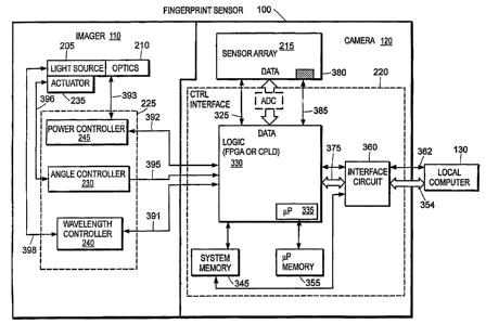
FIG. 2 is a hierarchical diagram of the fingerprint sensor 100. The
fingerprint sensor 100, as discussed in reference to FIG. l, includes a
fingerprint
irnager 110 and Engerprint camera 120. Each will be discussed in turn.
The fingerprint images 110 includes a light source 205, optics 210, and,
optionally, active control circuits/element(s) 225. The light source 205 may
be a
coherent light source, such as a laser diode, which works efEciently with a
HOE, or
may be a non-coherent light source. The optics 210 includes optical elements
250,
which are non-HOE's such as a slab waveguide, waveplate, polarizes, and
lens(es),
and at least one HOE, labeled 255 in FIG. 2, which includes a hologram.
The optional active control circuitlelement(s) 225 may include an angle
controller 230 and actuator 235. The actuator may be Direct Current (DC)
motor,
stepper motor, piezo-electric actuator, or other electro-mechanical device
capable
and adaptable-for use in moving the light source 205 to positions and/or at
angles
fine enough for use in the fingerprint sensor 100. A wavelength controller 240
may
also be employed in the images 110, where the wavelength controller 240 may be
used to change the wavelength of the light source 205, which, in turn, can
compensate for temperature-induced changes in the angle for the Bragg matching
condition of the HOE. A power controller 245 may also be employed by the
images
110 to control the output power and/or wavelength of the light source 205 for
controlling exposure levels of the fingerprint 115.
The fingerprint camera 120 includes a sensor array 215 and electronics 220.
The sensor array 215 may be a Charge Coupled Device (CCD) or Complimentary
Metal Oxide Semiconductor (CMOS) and have a plurality of pixels arranged in a
rectangular, or square pattern or other suitable pattern, providing a
resolution fine
enough for use in the fingerprint sensor 100. The electronics 220 are coupled
to the
sensor array 215 for receiving pixel data for processing. The electronics may
include, by way of example, a processor, memory, A/D conversion, circuitry for
variable shutter and/or integration time, and sensor data communications
interface.
CA 02529147 2005-12-09
WO 2005/001753 PCT/US2004/019917
-10-
It should be understood that the hierarchical diagram of FIG. 2 is merely
exemplary and could be configured in other ways and include additional or
fewer
components for implementing the principles of the present invention.
FIG. 3 is a generalized schematic diagram of the fingerprint sensor and
includes a subset of the components introduced in FIG. 2. The imager 110 of
the
fingerprint sensor 100 includes the light source 205 emitting a light beam
that
propagates into the optics 210. An actuator 235 may be mechanically connected
to
the light source 205, directly or indirectly, to steer the light beam into the
optics 210
in a controlled angular manner. Active control circuits) 225 provides) control
signals) to the actuator 235 and/or the light source 205 in accordance with
the
descriptions above in reference to FIG. 2. The angle controller 230 of the
active
controller circuits 225 may provide driving signals 396 to the actuator 235 in
order
to steer a light beam into the optics 210. The angle controller 230 may
receive
feedback signals 396 from the actuator 235, or feedback signals 395 from the
camera logic 330 for control or regulation purposes. The camera logic may be
composed of any collection of electronic processing circuitry that, by way of
example, may include one or more field programmable gate arrays (FPGAs),
programmable logic devices (PLDs), and/or microprocessors (~,P). The power
controller 245 of the active controller circuits 225 may provide driving power
signals 393 to the light source 205 in order to adjust the light intensity
incident upon
the optics 210. The power controller 245 may receive feedback signals 393 from
the
light source 205 or feedback signals 392 from the camera logic 330 for control
and
regulation purposes. The wavelength controller 240 of the active controller
circuits
225 may provide driving signals 398 to control the wavelength of the light
emitted
from the light source 205. The wavelength controller 240 may receive feedback
signals 398 from the light source 205 or feedback signals 391 from the camera
logic
330 for control and regulation purposes. .
In this embodiment, a feedback signal 391, 392, or 395 or any combination
thereof is presented to the active control circuits) 225 by the camera logic
330. As
in the case of typical feedback control systems, the feedback signals may be
generated by the camera logic 330 or by a microprocessor 335 as a function of
a
CA 02529147 2005-12-09
WO 2005/001753 PCT/US2004/019917
-11-
difference in actual signal level and a desired signal level corresponding to
imaging
performance.
For example, in the case of the fingerprint sensor 100, the feedback signal
395 may represent an angular error (i.e. mismatch from the Bragg matching
condition of the HOE for light of a particular wavelength incident to the HOE)
of the
light beam emitting from the light source 205 and projecting onto the
topological
surface of the fingerprint, which may be caused by temperature effects on the
optics
210. The camera logic 330 or microprocessor 335 may determine the feedback
signal 395 based on the image data from the sensor array 215. The image data
provided by the sensor array 215, for the purposes of feedback control, may
include
intensity data from a specific pixel in the sensor array, or data from a
grouping of
pixels in the sensor array or any combination thereof, or said image data used
for
feedback control may originate from at least one separate and independent
sensor
386, providing signal 387 to camera electronics 220 for feedback control, that
may
1-5 comprise a plurality of sensors. The sensor array 215 may contain an
additional
light sensitive area 380, separate from the array of imaging pixels in the
sensor array
215 and comprising one or more pixel, which may provide a signal 385 to the
camera electronics 220 for the purposes of feedback control.
The camera electronics 220 may also provide a control signal 325 to the .
sensor array 215 for use during imaging of the fingerprint features or other
topological features of the skin surface. The camera electronics may further
include
system memory 345 for storing image data following acquisition. The system
memory 345 may also provide support for storing image data or partial image
data
during processing of the fingerprint image. The camera electronics 220 may
further
include microprocessor memory 355 for supporting the microprocessor 335. The
microprocessor 335 and associated memory 355 may be used, for example, for
processing the image data or calculating the feedback parameters in order to
determine feedback signals 391, 392 or 395 or combinations thereof. Further,
the
camera electronics 220 may also include an interface circuit 360 for
communicating
with the local computer I30 via the communications link for transferring the
image
data 125 and fingerprint sensor control information 165 (see FIG. 1). The
interface
CA 02529147 2005-12-09
WO 2005/001753 PCT/US2004/019917
-12-
circuit 360 may communicate directly with the camera logic 330, with the
microprocessor 335, or the system memory 345, or any combination thereof.
FIG. 4 is a schematic diagram of one embodiment of the device of the
present invention. Light source 205 produces a beam of light 207, preferably
coherent. The light beam 207 enters a waveguide 405 at an angle relative to
entrance edge 604 and refracts towards bottom surface 612 of waveguide 405 and
is
guided through the waveguide 405 by total internal reflection (TIR) at the
substrate-
air interfaces such as shown in FIG. 4 by reflection of light path 1 to 1'.
The light
beam 207 encounters an interface between a Holographic Optical Element (HOE)
410 and waveguide 405, at which point, a portion of the light beam 207 is
diffracted
by the HOE at a near normal angle with respect to top waveguide surface 610
and
travels through cover plate 415 to the surface on which the finger 105 is
placed.
Referring to inset of FIG. 4, the surface topology of the skin being examined
(for
example a fingerprint) is labeled as 115. Said skin topology comprises
locations 420
that make contact with the top surface of the-fingerprint device (in this
embodiment
the top surface of cover plate 415) and other locations that do not make
contact with
the top surface of cover plate 415. At locations of non-contact 421,
diffracted light
422 is partially reflected at the cover plate-air interface and said reflected
light 423
is directed back through the HOE 410, through the substrate waveguide 405, and
on
to sensor array 215. Reflection at the interface of the cover plate 415 and
fingerprint
115 is suppressed at locations 420 where topological portions of the skin
surface,
such as ridge structure of the fingerprint, come into optical contact with the
cover
plate. Such topological portions that contact the cover plate are not limited
to ridge
structure of the fingerprint, but instead may comprise ridge structure of the
palm,
thumb, toe, other skin surface, etc. The remaining reflected light arising
from these
locations, such as diffuse reflected light from the topological surface
features of the
skin surface in contact with cover plate 415, carries an image of these
contact areas
to the camera 120.
It should be understood that while the embodiments of the devices of the
present invention, such as the one shown in FIG. 4, show waveguide 405 having
parallel top and bottom surfaces 610 and 612, other embodiments are
envisioned.
For example, in one embodiment, the waveguide can comprise a curved surface.
The
CA 02529147 2005-12-09
WO 2005/001753 PCT/US2004/019917
-13-
curved surface may be a cone, and a subject whose palm print is taken places
his or
her palm wrapped around the outer surface of the cone. In another embodiment,
the
waveguide is a cone having an inner surface accessible and a subject placing
his or
her forger in contact with such inner surface. Accordingly, as used herein,
the term
"top waveguide surface" generally refers to the skin-proximal surface of the
waveguide, i.e. the surface in contact with skin. As used herein, the term
"bottom
waveguide surface" refers to the sensor array-proximal surface of the
waveguide, i.e.
the surface opposite to the skin proximal surface.
Use of holographic optical elements (HOE) that comprise a photopolymer
recording media attached to at least one support layer allows for a compact
design
without sacrificing resolution. However, certain important characteristics of
the
holographic optical element are very temperature sensitive. For transmission
holograms, such as illustrated in FIG. 5, the fraction of light diffracted by
the
hologram depends both on the wavelength of the light, and its angle of
incidence 0
at-the interface-between HOE 410 and waveguide 405. Adequate diffraction
efficiency occurs only in narrow wavelength and angular ranges that are
determined
by the angles of the recording conditions for the HOE, the thickness of the
hologram
medium, and the wavelength of the light used for recording the HOE
(collectively
determine so called Bragg selectivity or Bragg matching condition), and the
wavelength of the light used to reconstruct the HOE. Without appropriate
adjustments to the wavelength or incident angle, temperature changes of only a
few
degrees will significantly reduce or even eliminate holographic diffraction of
a
single hologram due to the effect of temperature on the refractive index of
the
hologram, the grating spacing and the grating angle.
Refernng to FIG. 5, the intensity of diffracted light at temperature T = Tl
has
a peak at an incident angle 61 to the HOE for a specific wavelength ~,1. As
temperature changes from T = Tl to T = T2 to T = T3, the peak of intensity of
diffracted light at a fixed location along the z-axis shifts from an incident
angle 01 to
an incident angle of 02 to an incident angle 63, for a fixed incident
wavelength ~,1.
As a result, intensity of light diffracted to a fixed location z0 along the z-
axis
decreases, thus significantly degrading the signal-to-noise (SNR) ratio.
Similarly as
CA 02529147 2005-12-09
WO 2005/001753 PCT/US2004/019917
-14-
temperature changes from T = Tl to T = TZ to T = T3, the peak of intensity of
diffracted light shifts from use of a wavelength ~,1 to ~,2 to ~,3 for the
same incident
angle 01. A practical device for use in the field must either eliminate
operating
temperature variations, or compensate for temperature changes by changing the
incidence angle 0 of the light beam 1, or the wavelength or both, or provide
for
simple and fast alignment of angle 0.
Accordingly, in one embodiment, the present invention is an apparatus for
acquiring a fingerprint that compensates for operating temperature variations
by
automatically changing incidence angle (either a or 0 in FIG. 5) or wavelength
of
the propagating light to maintain adequate SNR at the sensor array.
Refernng to FIGs. 6A and 6B, one embodiment of the device of the present
invention is shown. A light source, such as a laser diode, 205 is positioned
in front
of a lens element 602, preferably at the focal point of lens element 602
(located a
distance f from lens element 602), Which in turn is held by mounting means 606
in
front of entrance edge 604 of waveguide 405. As used herein, the term "lens
element" refers to one or more elements having optical power, such as lenses,
that
alone or in combination operate to modify an incident beam of light by
changing the
curvature of the wavefront of the incident beam of light. Lens element 602,
for
example, can comprise more than one lens.
Both light source 205 and lens element 602 are mounted relative to platform
662. As the temperature of the ftngerprint sensor changes from T=Tl to T=Tz,
the
grating period, grating slant angle, and average index of refraction of HOE
410 will
change and, additionally, the index of refraction of the material comprising
waveguide 405 will change. Consequently, for a specific read wavelength ~,1,
the
required angle of incidence with respect to the surface normal 605 of the
entrance
edge 604 will change from al to a2 so as to maintain peak diffraction
efficiency of
the HOE 410 when temperature T changes from T=Tl to T=T2. To alter the
incident
angle one can choose length and thermal expansion coefficient of mounts 606
and
608 so that the relative difference in heights (in the y-axis) of the center
of the lens
element 602 and the center of the light source 205 change so that the incident
angle
CA 02529147 2005-12-09
WO 2005/001753 PCT/US2004/019917
-15-
of beam 207 changes from al to a2 at entrance edge 604 when T changes from
T=Tl
to T=T2. It may be shown that the following relationship for holds true:
~Z _ al _ CTEd Ll ~ CTE~L3 ~T , ( 1 )
where ~T = TZ-Tl, and CTEd and CTEI are the coefficients of thermal expansion
for
the light source (e.g., laser diode) mount and for the lens mount,
respectively.
It is understood that a material that expands as temperature increases
preferably also contracts as temperature decreases or vica versa. Thus, as
used
herein, the term "thermally expandable" means changing volume or length with
temperature.
Alternate embodiments of this general concept include, but are not limited to,
translating the lens element 602 in the y-direction, tilting waveguide 405 in
the y-z
plane, and/or moving and tilting a light source 205 provided that light source
205
outputs a collimated beam. In this latter embodiment, lens element 602 is
integrated
into the light source. 205. These motions can a11_ be achieved automatically
via
temperature induced changes in the dimensions of the structural elements that
form
the mechanical mounts for these optical components. These motions can be
performed in any combination and those skilled in the art will be able to
choose
proper materials and dimensions for said mechanical mounts.
Refernng back to FIG. 3 and to FIG. 6C and the inset, the fingerprint
apparatus of this invention further comprises an electronically controlled
actuator
390, such as a motor, that can be used to adjust the angle of incidence a by
changing
the vertical position of the lens element 602 with respect to the optical axis
of light
source 205, or by changing the vertical position of the light source 205 with
respect
to the optical center of lens element 602, such as shown in FIG 6C inset by
vertical
translation of the light source to a height position of y =~y at T=T2. As
depicted in
FIG. 6C, the electronic actuator is represented by two separate motors 620 and
621
that drive the laser source 205 and the lens element 602, xespectively in the
y-
direction to accommodate changes in incident angles at the entrance edge 604.
There
is a number of means by which the signal to drive the actuator can be obtained
by
one skilled in the art, and the methods depicted in FIG. 6C and its inset are
intended
to be illustrative but not limiting. In particular, it is desirable to use
light diffracted
CA 02529147 2005-12-09
WO 2005/001753 PCT/US2004/019917
-16-
by the hologram as the feedback source, since local temperature changes due to
contact with the finger or changes in the ambient temperature can thus
accounted
for.
For example, light ray 630 can refract into the waveguide to become light ray
630a. When light ray 630a diffracts in HOE 410, the diffracted beam 630b
propagates at near normal-incidence to surface 637 and encounters reflective
surface
633, at one or more locations on the skin contact layer 807, that reflects the
light
such that ray 630d is incident upon dedicated pixels 380 of sensor array 215.
Alternatively, ray 630d can be directed to a separate sensor array or to a
separate
detector, such as a photodiode, specifically included for this purpose.
Referring to
FIG. 6C, the feedback of the signals from pixels 380 or other sensor array or
detector can then be used to tune the incident angle a of the system.
Alternatively,
or in conjunction with this embodiment, the non-diffracted portion of the
light ray
630a is reflected at the interface of HOE 410 and skin contact layer 807 and
directed
towards a detector 635 positioned on or near edge 690 of the waveguide. In
still
another embodiment, a light ray 631 incident upon entrance edge 604 is
refracted
into light ray 631 a that diffracts at HOE 410, wherein the intensity of
diffracted
beam 631b is monitored by detector 634. The signals from detectors 634 and
635,
as with the signal from detector pixels 380, can be monitored and used to
optimize
the performance of the optical system. This ensures that despite temperature
fluctuations of the fingerprint sensor, the HOE remains Bragg-matched to the
light
source 205. In one embodiment, signals from reflection of the diffracted and
nondiffracted portions of light ray 630b and 630c can be monitored by separate
detectors and the difference signal normalized to the sum signal can be
obtained to
provide feedback information for both the magnitude and direction of
adjustment,
relative to a set point, that is required to compensate for temperature
changes. In
another embodiment, the intensity of the diffracted light that is incident
upon skin
contact layer 807 at other locations that are outside the area of the skin
surface being
examined, can also be monitored by placement of a detector at these other
locations
or at positions where the specularly reflected light from these other
locations can be
detected. The intensity of the undiffracted light may be monitored at
different
CA 02529147 2005-12-09
WO 2005/001753 PCT/US2004/019917
-17-
locations where its path of internal reflection is terminated by the presence
of
another surface, such as edge 690 of waveguide 405.
Alternatively, a second hologram, as well be detailed further in reference to
the description of FIG. 7A, included specifically for the purpose of
generating a
servo feedback signal, can be recorded so as to be located in the vicinity of
the main
hologram of HOE 410. In one embodiment, this second hologram can be co-located
with the main hologram by being co-locationally multiplexed.
Referring to FIG. 6D additional embodiments of the device of the present
invention are shown. Specifically, entrance edge 604 is designed so that the
incident
ray 630 refracts as ray 630a towards bottom surface 612 of the waveguide 405.
A
portion of bottom surface 612 of waveguide 405 can be coated with a reflective
layer (e.g. metal coating) labeled 614. Reflective layer 614 operates to
protect
waveguide 405 from smudges and other defects or contamination that may arise
on
bottom surface 612. These defects, if present, can add aberrations arid
regions of
non-uniform beam intensity in the reflected beam 630e, such as by suppressing
total
internal reflection at locations of the defects, thereby possibly compromising
the
quality of the image collected by sensor array 215. It is preferable that
reflective
layer 614 only extend as far as would be required to protect the area of the
first
reflection of the incident light at surface 612. The extent of reflective
layer 614 the
z-direction should not block rays such as ray 630d from reaching sensor array
2I5.
In another embodiment waveguide 405 includes light traps 655 at edge 690,
see FIG. 6D. Light traps 655 are designed to absorb substantially all of the
light
incident upon edge 690 and allow a minimum of light to reflect at edge 690.
Suppressing such reflections (for example ray 630e that is undiffracted by HOE
410)
minimizes the amount of spurious Iight that may illuminate the skin topology
under
examination and/or the amount of spurious light that is incident upon sensor
array
215, which would otherwise reduce the SNR of the fingerprint system.
In another embodiment, shown in FIG. 6E, entrance edge 604 operates with
optical power to optimize illumination of the location of the hologram of HOE
410.
In FIG. 6E, entrance edge 604 as shown includes optical element 660. In this
embodiment, lens element 602 (see FIGS. 6A-6D) can be eliminated. By way of
example, optical power of entrance edge 604 can be designed to provide optimal
CA 02529147 2005-12-09
WO 2005/001753 PCT/US2004/019917
-18-
illumination of HOE 410 for light sources 205 such as laser diodes that
operate to
output light with a certain divergence angle range BS.
Different algorithms can be used to implement the control of actuator 390
(see FIG. 3). Proper selection of a method of temperature compensation that is
particularly suitable for a fingerprint apparatus and the computer control
thereof will
be obvious to one skilled in the art. By way of example, it is sufficient to
set an
angle of incidence a once at a known temperature during an initial calibration
of the
apparatus. Then the actuator control can be instructed to move an element
under its
control in one direction in response to temperature-induced changes in the
Bragg
matching condition of the HOE and corresponding changes in the intensity of
the
diffracted light and illumination of sensor array 215 (see FIG. 4 and FIG.
6C). If
illumination is decreasing, then the direction of movement of the actuator can
be
reversed to find the optimal angle a corresponding to maximum diffraction
efficiency for the HOE. Once the detected intensity has traversed through a
peak as a
function of adjustment of angle c~ then the actuator can be returned to the.
position
that corresponded to the peak value of the detected illumination.
Alternatively, if
continuous compensation is preferred, then the actuator can be dithered back
and
forth traversing across the peak value of the detected intensity. In this
manner the
described algorithm controls the actuator so as to continually reverse
direction as it
crosses the peak value of detected illumination. It is preferable that dither
amplitude
be controlled such that the resulting intensity changes detected at the sensor
array
are sufficient for detection, but not so large that they deleteriously affect
the SNR of
the acquired fingerprint image.
In one embodiment, additional holograms are used to control the actuator.
In one embodiment, shown in FIG. 7A, two additional holograms 702 and 704 are
disposed at or near HOE 410. Holograms 702 and 704 are recorded so that their
peaks of angular Bragg selectivity are shifted in opposite directions with
respect to
the angle for Bragg matching HOE 410 (aHOE), as shown in FIG. 7B, and
correspond to incident angle a = a,L and a = aR for holograms 702 and 704,
respectively. Light beams diffracted from holograms 702 and 704 are detected
by
two dedicated sensors 720 and 722, respectively, or by dedicated areas of
sensor
array 215 (not shown). The dedicated sensors 720 and 722 are disposed (or the
CA 02529147 2005-12-09
WO 2005/001753 PCT/US2004/019917
-19-
locations of dedicated areas of sensor array 215 are selected), by way of
example, so
as to be located at positions along the z-axis to independently detect the
intensity of
light diffracted by holograms 702 and 704, respectively. Sensors 720 and 722
can
be located to detect the intensity of light diffracted by holograms 702 and
704 or
instead to detect the intensity of the diffracted light from said holograms
after the
diffracted light has reflected at top surface 726 of skin contact layer 807.
Preferably,
although not a requirement, ocL, ccHOE and ocR are adjusted so that the
intensities of
light beam diffracted by hologram 702 and 704 and detected by the respective
dedicated sensors are substantially equal at the values of incident angles for
the
Bragg matching condition of the respective holograms (shown as equal height
peak
in FIG. 7B). As can be seen from FIG. 7B, a,L < a,HOE < ccR. As the result, as
shown
in FIG. 7C, when the angle for the Bragg matching condition of HOE 410 and
holograms 702 and 704 changes due to temperature changing from Tl to TZ, the
dedicated sensors 720 and 722 will detect intensity of light beams diffracted
from
holograms 702 and 704 that are different from the respective intensities
detected at
temperature Tl for the same angle of incidence a. The difference in intensity
can be
used to compute the control signals 393 or 396 or 398 or combinations thereof.
It
should be understood that logic 330 is designed to receive signals from the
dedicated
areas for processing differences in intensities.
An alternative embodiment comprises use of multiplexed holograms
recorded in the photopolymer media of the HOE. The multiplexed holograms are
recorded so that the Bragg selectivity's of these holograms are substantially
overlapping. Use of multiplexed holograms that are recorded co-locationally
can
signiftcantly reduce the sensitivity of the apparatus of this invention to
temperature
changes, or alignment changes, or wavelength changes, or combinations thereof.
The multiplexed holograms, by way of example, can be multiplexed by the method
of planar-angle multiplexing in a manner such that the increment of the
recording
angle is less than the width of the Bragg selectivity of each multiplexed
hologram.
Alternatively, these holograms can be multiplexed by varying the interbeam
angle or
the wavelength such that the grating period of each multiplexed hologram is
slightly
different so that the angular or wavelength selectivity characteristics of one
such
CA 02529147 2005-12-09
WO 2005/001753 PCT/US2004/019917
-20-
holograms is partially overlapped with another. The optical convolution of the
multiplexed holograms provides a broadened detuning characteristic for the HOE
for
angle or wavelength, such that the diffraction efficiency of the element is
more
uniform when changes in wavelength, alignment, or temperature occur. This type
of
holographic element is advantageous compared to when the Bragg selectivity is
broadened by the approach of over modulation. Alternatively, thinner holograms
can
be used to broaden the angular selectivity characteristics.
In an alternative embodiment, changing the wavelength of the light generated
by a light source, while maintaining a constant incident angle a, can
compensate for
temperature-dependent changes in the Bragg condition of the HOE. In the
embodiments that utilize laser diode as light source 205, wavelength changes
can, by
way of example, be effected by changing the operating conditions of a laser
diode,
such as by changing the level of the driving current for the laser, or the
operating
temperature of the laser, or by temperature sensitive wavelength filtering of
a multi-
wavelength light source such as a LED.- Possible-wavelength filters include,
but are
not limited to, holographic optical elements whose properties will change in
concert
with the properties of the hologram of the waveguide.
Referring again to FIG. 3, an embodiment of the fingerprint sensor 100 that
can effect the wavelength change may utilize wavelength controller 240 to
adjust the
operating condition of the laser diode light source 205. The wavelength
controller
240 may adjust the operating current of the laser diode in order to change the
operating wavelength of the laser light source 205. Alternatively, the
wavelength
controller 240 may drive a heater or cooler element (not shown) in order to
change
the operating wavelength of the laser diode light source by way of controlling
the
operating temperature of the laser diode. The feedback signals provided for
controlling the operating wavelength of the laser diode may originate, for
example
from a thermocouple device attached to the laser diode. Alternatively, the
feedback
signals may originate from selected pixels, groups of pixels, or othex light
sensitive
areas 380 on the detector array 215, or any combination thereof. In the case
of the
aforementioned embodiment, the feedback signals that indicate light intensity
decreasing on the detector array may be processed by the camera logic 330 or
the
CA 02529147 2005-12-09
WO 2005/001753 PCT/US2004/019917
-21-
camera microprocessor 335 in order to determine the correct operating
wavelength
to drive the wavelength controller 240.
In other embodiments, rather than changing the wavelength, a light source
that has a broader wavelength spectrum can be used to reduce the sensitivity
of the
Bragg angle of the HOE to temperature change. Such light sources may include,
for
example, an LED or superluminescent LED. In these embodiments the incident
angle a, is held constant. As long as changes of the Bragg wavelength,
produced by
temperature changes of the HOE, are within the spectral bandwidth of the light
source there will be a sufficient intensity of diffracted light to produce
good
imaging.
Other embodiments of the apparatus of this invention relate to physical
construction of the device and will be described with reference to FIG. 6A. In
one
embodiment, entrance edge 604 of waveguide 405 forms an oblique angle to the
top
and bottom surfaces 610 and 612, said surfaces 610 and 612 being substantially
parallel and planar surfaces. Use of-an oblique angle for the entrance face-of
the
waveguide advantageously reduces the thickness requirement for said slab
waveguide. For example, with use of oblique angle for the entrance face, light
beam
630 can be refracted directly towards top surface of waveguide 610 rather than
towards bottom surface of waveguide 612 as it does in FIG. 6D. Refracting
incident
light 630 directly towards top surface, thereby eliminating the total internal
reflection condition that is otherwise required for bottom surface of
waveguide 612,
reduces the z-dimension of waveguide 405. Alternatively, waveguide 405 can
comprise inner and outer surfaces that may be curved so that a large
topological
surface of the skin can be placed on the outer surface at one time and imaged,
such
as could be the case when imaging the topological features of the surface of a
palm.
Again, use of an oblique angle for the entrance facet of the waveguide
advantageously reduces the thickness requirement for said waveguide.
Other embodiments of the apparatus and method of this invention relate to
the hologram recorded in the photopolymerizable media of the HOE. Referring to
FIG. 8A, the apparatus of this invention preferably comprises HOE 410 that
diffracts
light (beam 826) in a direction that is not perpendicular to skin contact
layer 807 so
that the light reflected at the interface of skin contact layer 807 with air
will not be
CA 02529147 2005-12-09
WO 2005/001753 PCT/US2004/019917
-22-
diffracted by HOE 410 on the return path toward the imager (ray 827). More
preferably, HOE 410 diffracts light in a direction that differs from the
perpendicular
direction by an angle that exceeds the angular width of the Bragg selectivity
of the
HOE, but said angle is additionally as close to perpendicular as possible in
order to
5, minimize distortions in the imaged fingerprint by keeping the optical path
length
(OPL) from the skin to the sensor as short as possible. A preferred
diffraction
property of the HOE can also be achieved with multiplexed holograms or with
overmodulated holograms providing for both the preferred angle of the
diffracted
light and also the preferred broadened angular selectivity of said hologram.
Another aspect of the apparatus and method of this invention, is that HOE
410 comprises one or more holograms that operate as a holographic grating to
redirect the light from waveguide 405 towards the finger in a direction that
differs
from the perpendicular direction by an angle that exceeds the angular width of
the
Bragg selectivity of the one or more holograms, and that said holograms) is
also
- 15 formed-to operate-with a diffraction efficiency of at-least 10%, -more
preferably at
least 50%, even more preferably at least 75%, and most preferably greater than
90%.
In the embodiment shown in FIG. 8, a 1/2 wave plate 819 is included between
light source 205 and entrance edge 604 of waveguide 405 to rotate the plane of
polarization of the light beam such that the polarization is matched to the
polarization that HOE 410 is tuned to while at the same time providing optimal
illumination of entrance edge 604 of waveguide 405. Half wave plate 819 can be
v
tilted on an axis perpendicular to the optical axis of the incident light in
order to
provide an effective optical thickness or optical path length (OPL) for phase
change
that is increased if necessary to be optimal for the wavelength of light
source 205.
In another embodiment, shown in FIG. 8C, skin contact layer 807 comprises
a curved layer 807A that, by way of example, can be a plano-convex lens.
Curved
layer 807A can, for example, be used to capture larger images and enhance
signal
strength. In another embodiment curved layer 807A is a separate optical
element that
is attached to skin contact layer 807 or is placed on top of skin contact
layer 807
when the fingerprint is captured.
In another embodiment, skin contact layer 807 includes a compliant or
pliable polymer coating (not shown). The pliable coating can, by way of
example, be
CA 02529147 2005-12-09
WO 2005/001753 PCT/US2004/019917
- 23 -
attached to skin contact layer 807, or it can be part of the cover plate, or
it can be
placed onto the cover plate before the fingerprint is captured. The pliable
coating
can be used to enhance image quality and reduce the dependence of SNR in the
acquired fingerprint image on finger moisture or the wetting characteristic of
the
finger surface to skin contact layer 807 by improving the degree of optical
contact
between the surface topology of the skin of the finger and the skin contact
layer.
In another embodiment skin contact layer 807 is formed from a material that
has a refractive index that optimizes SNR of the captured image, such as fused
silica, whereby the refractive index of the contact surface is similar to that
of the
I O surface of the finger or other skin surface.
Referring to FIG. 8D, the devices of the present invention can also include
additional optical components. In one embodiment, the present invention
includes
wave plate 838, preferably'/4 waveplate, in combination with linear polarizer
840 to
reduce detection of noise that can arise undesirably from sources such as
diffuse and
I 5- specular reflection. In this manner the contrast of the fingerprint image
can be
improved. In one configuration, 1/4 wave plate 838 can be sandwiched between
HOE
410 and skin contact layer 807 or 807A (see FIG. 8C), and the linear polarizer
840 is
located between waveguide 405 and above sensor array 215. When linearly
polarized light is diffracted from HOE 410 in a direction of 1/4 wave plate
838, the
20 polarization is transformed upon propagating through 1/4 wave plate 838 to
circularly
polarized light. Upon reflection from either the top surface 726 of skin
contact layer
807 or 807A or from ridge structure of the finger, the circularly polarized
light is
transformed by 1/4 wave plate 838 back into linearly polarized light that has
an
electric field direction that is orthogonal to the original direction of the
light entering
25 HOE 410. When light, diffracted by HOE 410, interacts with the ridge
structure of
the finger surface that is in contact with the top surface 726 of skin contact
layer 807
or 807A, both diffuse and specular reflections occur, with the former being
stronger
in some embodiments. When the diffracted light interacts with the top surface
726
of skin contact layer 807 or 807A at locations that correspond to a portion of
skin
30 surface that does not touch top surface 726 at these locations, only
specular reflected
light occurs. Detection of the noise contributions from the reflected light
can
substantially increase the level of grey-scale detected for portions of the
captured
CA 02529147 2005-12-09
WO 2005/001753 PCT/US2004/019917
-24-
fingerprint that would otherwise most desirably be zero-grey scale level or
black.
High grey-scale levels for areas of the fingerprint image that otherwise
should be
black can substantially reduce contrast in the captured image and thus make
image
analysis more difficult. The diffuse reflected light can be partially to fully
depolarized, and thus polarizer 620 can be oriented to at least partially
block
contributions of the diffuse reflected light from being captured by sensor
array 215,
thereby improving contrast. Linear polarizer 840, can be used to improve SNR
by
being positioned between skin contact layer 807 and sensor array 215.
It has been found that selecting a wavelength emitted by light source 205 that
is in a range of wavelengths that are effectively absorbed by the finger
(e.g., blue
light with ~, <less than about 460 nm ) reduces diffuse reflected light,
thereby
improving contrast.
It has been further found that additional improvements in SNR can be
achieved by use of antireflection (AR) coatings on any of the surfaces that
may
reflect light other than skin contact layer 807: Those skilled in the art can
select from
a number of possible stacks of two-layer and multilayer films of different
materials
with different values of refractive index to provide for adequate
antireflection
performance. Typical AR coatings can achieve reduction in reflectivity to less
than
0.1 % at +/- 10° from the normal to the surface of the coating.
Similarly, use of
transparent dielectric layers, that, by way of example, can be flexible
polymeric film
materials such as silicones or siloxanes characterized by having a low glass
transition temperature, to eliminate air gaps between surfaces that reflect
light at the
interface with air, can improve SNR further by operating to substantially
reduce the
intensity of the light that originates from reflections) at interfaces
between, for
example, the waveguide substrate and air, or the linear polarizer and air, or
the cover
glass on the sensor and air or combinations thereof.
A preferred embodiment of the present invention will now be described with
reference to FIG. 8A (side view) and FIG. 8B (top view).
The fingerprint device, depicted in FIG. 8A is composed of housing 818 that
contains a light source 205. Light source 205 may contain one or more light
sources
that include a white light source such as a tungsten lamp, but preferentially
light
source 205 includes of one or more low-cost, high-efficiency sources such as
light
CA 02529147 2005-12-09
WO 2005/001753 PCT/US2004/019917
- 25 -
emitting diodes (LEDs) and/or semiconductor laser diodes. For reduced opto-
mechanical alignment tolerances and simpler diffractive grating designs for
HOE
410, it is desirable to collimate the radiation emitted from the light source.
Lens
element 602 is shown in FIG. 8A. Although a single transmissive lens is
depicted,
in general lens element 602 is composed of any combination of one or more
transmissive and/or reflective optical elements such that the net optical
effect is a
substantial collimation of radiation emitted by light source 205. The
collimated light
emerging from lens element 602 is incident upon entrance edge 604 of waveguide
405. The angle cpSB of the entrance edge 604 is specified so that optical axis
804 of
the incident light beam propagating at an angle ~1 (relative to the z-axis) is
refracted
at entrance edge 604 so that beam 822 propagates at an angle 0SB with respect
to the
normal to the interface between waveguide 405 and HOE 410. As a result, a
sufficiently large footprint of light illuminates HOE 410 and therefore
illuminates
finger 105 or other topological surface of the skin. ,
15- Referring to FIG: 8A; thickness T is defined as the distance that
separates the
top 726 of skin contact layer 807 to surface 814 of sensor array 215. For
compactness of the device and in order to reduce the thickness T, which plays
a role
in defining the spatial resolution of the fingerprint sensor, it is desirable
that the
angle 0SB be large, for example greater than about 70° but it is
preferable that ASB be
less than about 80° for otherwise the device will exhibit large
sensitivity to thermal
changes. By way of example, for ASB = 79° and a substrate block of
thickness
TSB = 3.3 mm approximately 17 mm [3.3~tan(79°)] length of the skin
topology can
be imaged in the z-direction. For the case of 0SB = 79°, then with 01 =
17.5°, and the
substrate block composed of a material of index 1.53, cpSB = 90.9°.
Note that by
having light source platform 662 tilted below the horizon, the opto-electro-
mechanical components of the fingerprint sensor are allowed to lie below skin
contact layer 807, thereby allowing for the housing 818 to be flush with said
cover
slide top.
Continuing to refer to FIG. 8A, the light, incident upon waveguide 405/HOE
410 interface, is refracted into HOE 410. In one embodiment, holographic
grating
of HOE 410 is a volume grating. One skilled in the art can design and engineer
a
CA 02529147 2005-12-09
WO 2005/001753 PCT/US2004/019917
-26-
surface-relief grating that would function similarly. Generally transmission
volume
holograms and surface relief gratings are polarization sensitive, and thus
diffraction
efficiency of the hologram can be significantly reduced when reconstructing a
hologram with, for example, p-polarized light, if the grating is designed for
s-
polarized light. Polarization insensitive volume holograms, however, can also
be
recorded in materials that are sufficiently thick or exhibit large refractive
index
modulation or combinations thereof, and such holograms can also be used in the
apparatus of the present invention. The diffracted beam 826 is propagating in
a
direction that is preferentially close to normal to surface 726 of skin
contact layer
807, but at an angle different from the normal by at least the angular width
of the
Bragg selectivity of the volume grating in HOE 410. Diffracted beam 826
propagates through skin contact layer 807 and towards surface 726 and forger
105.
The reflected beam 827 transmits back through skin contact layer 807 and HOE
410.
Since reflected beam 827 is not Bragg-matched to the volume grating of HOE
410,
1-5 minimal-light loss occurs a-fter,transmission through HOE 4-10. Diffracted
beam 826
is propagating in a direction substantially close to the y-axis such that the
optical
path length (OPL) of reflected beam 827 from surface 726 to detector surface
814 is
minimized. The OPL of reflected beam 827 is critical in determining the
resolution
of the device since there are no optical elements providing for imaging of top
of
surface 726 onto detector surface 814. Therefore, the longer the OPL of
reflected
beam 827, the more blurred features of finger'105 (or other skin topology
being
examined) will become due to diffraction effects. Light from a collimated
monochromatic light source will reflect and scatter from features of the
surface
topology of the skin surface, wherein said light will diverge with propagation
distance from the feature after an OPL of one Fresnel length, lf, expressed in
terms
of the area of the feature, w2, and the wavelength, ~,, as
of -_ s~. (2)
For pores in fingerprints, the Fresnel length is on the order of 1 mm for the
smallest
and about 14 mm for the largest. Consequently shortest possible OPL is
critical to
resolving finer details of small topological features of the skin surface,
such as pore
or ridge contour information in fingerprints, palm prints, etc.
CA 02529147 2005-12-09
WO 2005/001753 PCT/US2004/019917
-27-
In one embodiment, there are several films, 810, 811 and 812, disposed
between waveguide 405 and detector cover 813. These films may be arranged in
many different manners, but their purpose serves to suppress reflections of
light, in
addition to filtering out unwanted noise. In one embodiment, film 810 is a
linear
polarizer film. Polarizer 810 preferentially has a polarization orientation
substantially parallel to the polarization of the incident light ray 822. As
such,
polarizing film 810 suppresses portions of diffracted beam 826 that are
scattered by
finger 105 (and hence depolarized) from reaching sensor array 215. Film 811 is
a
wavelength filter. Wavelength filter 811 is preferentially tuned so that it
substantially transmits wavelengths of light emitted by light source 205, and
blocks
all other wavelengths, and as such rejects ambient light originating outside
of the
housing 818 that would otherwise be incident upon sensor array 215. Film 811,
by
way of example, can be a dichroic film coating or a material that absorbs the
desired
spectral distribution of the ambient light, such as can be the case for a dyed
plastic.
Note that-the wavelength-filtering properties of film 811 can be incorporated
into the
bulk material or as a coating on either waveguide 405, skin contact layer 807,
and/or
detector cover 813, thereby eliminating the need for wavelength filter 811.
Film 812
is an index-matching material where the index of refraction of said material
preferentially matches within about 0.15 to the index of refraction of film
811 and
detector cover 813. As a result, the intensity of reflected light at the
interfaces of
film 812 is not greater than about 0.25% of the intensity of the incident
light at the
boundaries of fllrn 812. Alternatively, if index-matching material is not
desired, it is
preferred that the space shown occupied by film 812 be replaced by a small air
gap
(for example, approximately 0.1 to 0.2 mm) and that the film 811 and detector
cover
813 each have an anti-reflection (AR) coating on their two opposing surfaces.
The light transmitted by detector cover 813 is incident upon sensor array
215. In one embodiment, sensor array 215 comprises a plurality of detector
elements that enable a 2-D image of the fingerprint to be captured. Sensor
array 215
can be a 2-D or 1-D charge coupled device (CCD), but is preferentially a
detector
requiring Iower electrical power such as a 2-D or 1-D CMOS device. For the
reduction of stray light, which for a coherent light source can lead to the
creation of
interference fringes that may be mistakenly construed for features on the skin
being
CA 02529147 2005-12-09
WO 2005/001753 PCT/US2004/019917
-28-
examined, one preferentially has an AR coating at the detector cover 813
surface
that faces the sensor array 215. Sensor array 215 is mounted to a circuit
board 805
that may can contain other electronic circuitry designed for the analysis of
the
acquired images, such as the circuitry that includes the camera electronics
220, the
controller circuits 225 or any combination thereof. The processed data is sent
via
cable 820 to bulk-head connector 821 that allows the fingerprint sensor to
transmit
data 125 and control functions 165 to a host computer 130. Bulk-head connector
821 and cable 820 are preferentially used to transmit the power to the power-
consuming elements of the device of the present invention. In one embodiment,
a
wireless transceiver/transmitter pair can be integrated into the device of the
present
invention for transmission of data a remote host.
In one embodiment, skin contact layer 807 preferentially maximizes the
contrast ratio between the ridges and valleys of the skin being scanned. The
valleys
of the skin in contact with skin contact layer 807 do not touch top surface
726,
resulting in diffracted-beam-826 reflecting at the resulting interface between
top
surface 726 with air. To maximize contrast between the ridges and the valleys,
in
one embodiment, top surface 726 of skin contact layer 807 is made of a
material that
has a low index of refraction that preferentially matches the index of
refraction of
the skin surface at the wavelengths emitted by light source 205. Although
polymer
materials such as silicone can be used to match the index of refraction of the
skin
(n ~ 1.36) well, these materials are not durable and will wear easily in use.
Materials with low indices of refraction such as fused silica (nD = 1.458),
Corning
PyrexTM (1.474) or Schott BoroFloatTM 33 (1.471) are preferred as they are
harder
and can withstand more use without, for example, being scratched or marred. In
another embodiment, skin contact layer 807 is coated with an optical thin-film
stack.
This thin-film stack can be designed by one skilled in the art such that the
reflectivity at the wavelengths emitted by light source 205 are minimized for
the
interface between skin contact layer 807 and the skin, but is maximized for
the
interface between skin contact layer 807 and air. In another embodiment this
thin-
~ film stack is designed by one skilled in the art such that the reflectivity
at the
wavelengths emitted by light source 205 are maximized for the interface
between
CA 02529147 2005-12-09
WO 2005/001753 PCT/US2004/019917
- 29 -
skin contact layer 807 and the skin, but is minimized for the interface
between skin
contact layer 807 and air.
FIG. 8B depicts a top-down view of the embodiment of the device shown in
FIG. 8A. In one embodiment, the Width of the beam in the x-direction
illuminating
waveguide 405 and hence the illuminated width of finger 105 is dictated by the
width of the beam that enters lens element 602. For the embodiment of light
source
205 containing at least one semiconductor laser, the divergence of a
semiconductor
laser diode is anamorphic. With such an anamorphic beam, the angle of rays 823
(see FIG. 8A) and 824, emerging from light source 205 and representing the 50%
drop in intensity level of the beam, will make angles of 65 and 6f,
respectively, with
respect to optical axis 804. For typical laser diodes, the ratio of these two
angles is
approximately 3:1, which means the beam is substantially elliptical in a cross
section
perpendicular to optical axis 804.
By way of example, consider the specification that the fingerprint device
mustbe capable of examining a 17 x 1-7 mm area of skin. As illustrated
earlier; a
thickness TsB of 3.3 mm can accommodate the 17 mm skin size in the z-
direction.
To accommodate the 17 mm in the x-direction, the waveguide must be at least
17 mm wide in this direction (as does the beam width of light in the x-
direction from
light source 205 that (illuminates entrance edge 604). Therefore entrance edge
604 is
substantially rectangular having dimensions in x and y of 17 mm and 3.3 mm,
respectively. For maximum light efficiency, it is preferable that the fast
axis of the
laser (e.g., the axis of the laser that diverges the fastest), with full width
at half
maximum (FWHM) of 20f, be in the direction of the l7mm width of waveguide 405
(corresponding to the x-axis). Likewise, the slow-axis (axis of the laser that
diverges
the slowest) having FWHM of 20s, will correspond to the direction of the 3 mm
thickness of waveguide 405.
In addition to the mechanical matching of beam widths and footprints for the
area to be imaged of the topological surface of the skin, use of a diffraction
optical
element 410, that operates to diffract light so as to illuminate said surface
of the
skin, is generally polarization dependent. Consequently, use of correct
polarization
is preferred to achieve good SNR of the system. For a single transverse mode
laser
CA 02529147 2005-12-09
WO 2005/001753 PCT/US2004/019917
-30-
diode, the polarization of the laser diode will be perpendicular to the fast
axis. For a
laser diode oriented for optimized light transmission through entrance edge
604 (see
FIG. 8A), the polarization of the collimated laser light will be TM-polarized
(magnetic field polarized perpendicular to the plane of incidence) relative to
the
boundary between waveguide 405 and HOE 410. Therefore, in one embodiment,
HOE 410 is designed fox TM-polarized light. If the diffration grating of HOE
410
has peak diffraction efficiency for TE-polarized light (electric field
polarized
perpendicular to the plane of incidence), then some means of rotating the
polarization of the electric field that is incident upon entrance edge 604 is
required.
Though one skilled in the art can use any of the numerous ways of rotating the
polarization that include the use of birefringent prisms, cascaded linear
polarizers, or
cascaded mirrors, the preferred method uses a wave plate 819, preferably a
half wave plate, to rotate the TM-polarized light of diode to TE-polarized.
It is known in the art that a volume grating can be theoretically designed for
high diffraction efficiency for TE polarization, TM polarization, or for
random
polarization. The condition for peak diffraction efficiency (r~~100%) in a
lossless
dielectric thick volume grating can be derived using two-wave coupled-wave
diffraction theory. See H. I~ogelnik, "Coupled Wave 'Theory for Thick Hologram
Gratings," Bell Syst. Tech. J. 48 (1969), pp. 2909-2947, the entire teachings
of
which is herein incorporated by reference. Fox TE-polarized light the
condition on
the index of refraction modulation gal and the thickness of the grating d is
given by
nIdITEoptimized Cfn+2Ja, COSBCCOSB-nC051~~,
where ~, is the free-space wavelength, 0 is the angle of incidence in the
volume
medium, and ~ is the slant angle of the grating vector K of the grating with
respect
to the surface normal of the volume layer, and na is a non-negative integer.
For TM-
polarized light, the condition on n1 and d is given by
1 cosBCcosB- n cos~~
jZIdITMoptimized -CnI+2~~ COS2(8'~)] (4)
It is also possible to record a hologram that is polarization independent. One
example of a method fox recording such a hologram is disclosed in a Published
U.S.
CA 02529147 2005-12-09
WO 2005/001753 PCT/US2004/019917
-31-
Patent Application US 2003/0007201, the teachings of which are herein
incorporated by reference in their entirety. Briefly, the diffraction
efficiency of a
hologram is a periodic function of the value of the grating strength of the
hologram,
which is dependent upon a material property, namely the value of its
refractive index
modulation. For photopolymer recording materials, the refractive index
modulation,
in turn, depends primarily on the degree of chemical segregation achieved in
the
recording material of the polymerizable component and the binder and the
relative
refractive index difference between the polymerizable component and the binder
in
the recording material, but it also may depend on thickness of the recording
material,
angles of incidence of the beams used to record the hologram and thereby the
grating period, as well as the wavelength of the light used to record the
hologram.
For a given refractive index modulation achieved by the recording material,
the
grating strength is dependent upon similar parameters such as grating period,
thickness, and wavelength. A hologram is optimized for a particular
polarization
1-5 - when it is recorded using-such combination of the above parameters that
the
resulting value of refractive index modulation corresponds to a peak of the
diffraction efEciency. Ordinarily, the peaks of diffraction efficiencies of
the
holograms optimized for s- and p-polarized light do not occur at the same
values of
the refraction index modulation or grating strength (i.e. same values of the
above-
mentioned parameters). However, using the periodicity of the diffraction
efficiency
as a function of the value of the refractive index modulation or grating
strength, it is
possible to record a hologram that is optimized for both s- and p-polarized
light.
Since any light wave can be described as superposition of s- and p-polarized
waves,
a hologram that is simultaneously optimized for s- and p-polarized light is
said to be
polarization independent.
In the preferred embodiment of the device of the present invention, beam
blocks 816 and 817 are integrated into the design. Beam block 816 is designed
such
that light from light source 205 does not enter sensor array 215 or any of the
film
layers, 810 through 812. Beam block 817 is designed so that light from light
source
205 does not impinge onto finger 105, HOE 410, or skin contact layer 807. Both
beam blocks 816 and 817 are positioned as close to entrance edge 604 as
possible in
order to minimize adverse diffraction effects due to the clipping of the light
beam,
CA 02529147 2005-12-09
WO 2005/001753 PCT/US2004/019917
-32-
collimated by lens element 602, by edges before the light beam reaches
entrance
edge 604. By incorporating beam blocks 816 and 817 into the device, the amount
of
stray light reaching sensor array 215 is reduced.
For a volume grating, the angle of incidence of light on the grating is
critical
since, due to Bragg selectivity, light incident at incorrect angles will not
be
diffracted or will be diffracted less efficiently. The embodiment shown in
FIG. 8A
and FIG. 8B allows for adjustment, manual or otherwise, such as by use of
control
circuits with controllers and actuators, of the angle of incidence of beam 822
onto
HOE 410.
In this embodiment, there is provided laser platform 803 that is mechanically
constructed such that it pivots about the center line 806 of entrance edge
604. The
pins 839 are aligned with the centerline 806 and over said pins are place
sleeves 840
that are coupled to the laser platform 803. Though not drawn, springs and
adjustment screws are preferentially attached to laser platform 203 so that
the
-15 orientation of laser platform-203 can-be set. In this manner,-~1 can be
tuned, such as
manually with use of feedback from sensor 215 or other sensors or detector, or
by
use of actuators with controls circuits and actuators, while maintaining the
alignment
of optical axis 804 relative to the center of entrance edge 604. By tuning 01,
one
tunes 0s$ and therefore the angle of the light incident upon HOE 410, thereby
allowing for the tuning of maximum diffraction efficiency by the volume
grating.
During the operation of the device of FIGS. 8A and 8B, light beam from
source 205 is anamorphically expanded, i. e. only one axis of the crossection
of the
beam emerging from lens element 602 is expanded by propagating through
waveguide 405 and diffracting on HOE 410 Refernng to FIG. 9, the use of a
grazing incidence reflection grating 904 allows anamorphic expansion of a beam
of
diameter D~ to a beam of diameter Dr along the x direction. As depicted,
reflection
grating 904 has a reflective grating surface 900 whose features are designed
such
that the first-order diffracted beam 901 enters entrance edge 604 (not shown)
parallel to the z-direction.
CA 02529147 2005-12-09
WO 2005/001753 PCT/US2004/019917
-33-
The grating geometry of FIG. 9 has the advantage that beam expansion in
the xz plane is accomplished. The achieved beam expansion of the incident beam
of
diameter D; is given by
D,. _ cos 9_1
Dt cos 81 ' (5)
where A_I is the angle of the diffracted -1St order reflected beam 901
measured
relative to the grating surface normal 902 and 01 is the angle of incidence of
the
incident beam 903 relative to grating surface normal 902.
As an example of such a reflective anamorphic beam expanding grating,
consider a 1600 lp/mm reflection grating. Consider further that light source
205 is a
semiconductor diode laser of 655 nm wavelength radiation and that beam 903 is
incident upon said 1600 lp/mm reflection grating at 8; = 85°. The
resultant
diffracted negative first order propagates at 0_1 = 2.97 and the expansion
ratio DrlD;
achieved is 11.5. Note that one skilled in the art can design and engineer
other
gratings (for example, surface-relief or volume), including gratings wherein
the
incident beam 903 transmits through a substrate such that it illuminates the
grating
from inside of the substrate material (for example a glass) which then
transmits the
required diffraction order for achieving the level of anamorphic beam
expansion
required. Whether a transmission or a reflection grating is designed to
perform the
required anamorphic beam expansion in the xz plane, it is preferable that the
grating
have a sufficiently high frequency such that a minimum number of diffraction
orders
propagate other than the order of interest. In this manner, one can make the
distance
between the grating 904 and the waveguide 405 as short as possible such that
only a
single diffraction order enters into the substrate block.
In the embodiment shown in FIG. 9, the diffracted beam 901 travels
substantially parallel to the z-axis. The geometry of the fingerprint sensor
illustrated
in FIGS. 8A and 8B indicates the preference for a HOE 410 that has grating
fringes
that are primarily tilted in the y-z plane, but are approximately uniform
along the x-
direction. As such, HOE 410 has Bragg-matching conditions that require
fractions
of a degree of control of the light propagation angle in the y-z plane, but
less
stringent (>5 degrees) requirements for the angle of light propagation in the
x-z
CA 02529147 2005-12-09
WO 2005/001753 PCT/US2004/019917
-34-
plane. Consequently, mechanical alignment of the beam emerging from lens
element 602 has larger tolerances in the x y plane than in the y-z plane.
For optimal performance of the device of the present invention, it is
preferred
that the device be athermalized, i.e. capable of temperature compensating, as
described above. One skilled in the art can model the effect of temperature
changes
on the ray paths of light entering the waveguide and the HOE, respectively,
and
derive relationships between the material properties of the HOE and the
waveguide
in order to achieve athermalization. From this analysis, one skilled in the
art will
conclude that HOE 410 and waveguide 405 and/or skin contact layer 807, should
preferably be constructed from material that has substantially similar
coefficients of
thermal expansion or thermo-optic coefficients or both. As used herein, the
term
"thermo-optic coefficient" refers to the value of the derivative of the
refractive index
n = fa(T) with respect to temperature T, i.e. draldT. By way of example, for
an HOE
constructed from a photopolymer having a dn/dT of -2.O.x 10~, one would
preferentially choose the moldable plastics Zeonex-E48R (dn/dT=-1.0 x I0~) or
Zeonex 3308 (dn/dT= -1.2 x 10~) over glass such as BK7 (dn/dT=3.0 x 10-6).
Alternatively, the device can be athermalized by use of a heater that
maintains the
HOE at constant temperature. In still another embodiment the device may
comprise
a second light source emitting at a different wavelength from light source
205,
whereby said second Iight source operates so as to be adsorbed by a material
in HOE
410 and thereby maintain the temperature of HOE 410 at a suitably constant
termperature.
EXEMPLIFICATION
A fingerprint of the forefinger of the right hand of one our staff was
recorded
in 1996 using the optical design shown in FIG. 4. Total image area captured of
said
fingerprint was approximately 0.15 x 0.15 inches. The fingerprint as captured
was
displayed on an analog video monitor and a black and white photograph of the
image was obtained using a Polaroid instant camera with high contrast black
and
white ~Im. Subsequently, said photograph of said fingerprint was stored under
ambient conditions.
CA 02529147 2005-12-09
WO 2005/001753 PCT/US2004/019917
-35-
In 2003, 6.5 years later, said Polaroid photographic image was digitized by
scanning at 600 dpi, and used as a training template for an example of the
fingerprint
correlation software of this invention. A new image of the same finger was
acquired
in 2003 using a fingerprint imager of this invention comprising the optical
design of
FIG. 4. The captured fingerprint was compared to the scanned image of the 6.5-
year-old photograph of the original fingerprint. A positive identification,
using
locations of pores, the fine detail of the ridge contour at the boundaries of
ridges and
valleys, and minutiae was readily achieved, even though the said original and
new
images represent a finger area only 1/8" by 1/8", scale and rotation were
different,
the photograph had distortions due to being obtained from an image of the
original
fingerprint as displayed on a curved surface of a video monitor, and contrast
and ~
exposure were not matched nor calibrated in any way. At least 50 features,
including
45 pores and 5 minutia points were captured from the original scan of the 1996
image, of which 22 pores and 5 minutia were present, detected and matched in
the
captured fingerprint imaged in 2003. The-successful correlation results show
that
including pores in the fingerprint as well as the fine details of the ridge
contoux, by
use of an apparatus that is capable of acquiring fingerprint images at high
resolution,
greatly increases the number of features that can be used for image
correlation and
significantly enhances the reliability of fingerprint comparison. Beneficial
effects of
the enhancements provided by the apparatus and method of this invention
provide
for reducing the occurrence of false acceptance, improving (through use of
multiple
templates) false reject rates, and significantly reducing the fingerprint
sample area
required for positive unique and deterministic authentication and
identification.
FIG. 10 shows the Bragg detuning characteristics for 8 co-locationally
multiplexed slant fringe plane-wave holograms recorded in 50 micron thick USLH-
500-7A Aprilis holographic recording medium. Recording was carried out in the
conventional manner using angle multiplexing where the increment of the
recording
angles for each of the co-locationally multiplexed holograms corresponds to
twice
the value for the full angle width at half height of the respective Bragg
detuning
curves. Each hologram was recorded with equal beam intensities of 4 mW in the
Reference and Signal beam paths using spatially filtered and collimated light
with a
fixed value for the interbeam angle of 48.6°, and the sample was
rotated about the
CA 02529147 2005-12-09
WO 2005/001753 PCT/US2004/019917
-36-
vertical axis by increments of 2° for each subsequent recording.
Recording times
used for the sequential recording of the co-locationally multiplexed hologram
were
varied in order to achieve similar diffraction efficiency for each of the
holograms, as
the recording sensitivity of the multiplexed holograms were about 27, 30, 24,
16.75,
15.65, 7.9, 4.2 and 1.2 cm/mJ, respectively, for holograms #1-#8. The
cumulative
grating strength for the 8 multiplexed holograms corresponds to the case where
v/~ ~, and thus a substantially overmodulated hologram could have been
recorded
as a single plane-wave hologram.
When the separation angle between the multiplexed holograms is reduced to
an increment equal to the full width at half height of the Bragg detuning
curve, then
the resultant Bragg selectivity curves of the holograms are convoluted as
shown in
FIG. 11. The range of diffraction efficiency shown in FIG. 11 as a function of
the
value of Bragg detuning angle was not optimized for achieving a more desirable
top
hat type manifold. Nevertheless, the results in FIG. 10 and FIG. 11 are
illustrative of
the use of multiplexed holograms to provide for a means of compensating-for
temperature variations of the fingerprint device.
While this invention has been particularly shown and described with
references to preferred embodiments thereof, it will be understood by those
skilled
in the art that various changes in form and details may be made therein
without
departing from the scope of the invention encompassed by the appended claims.