Note: Descriptions are shown in the official language in which they were submitted.
CA 02529245 2008-11-10
PROCESS TO FORM COMPOUND WITH INDOLOCARBAZOLE
MOIETIES
BACKGROUND OF THE INVENTION
[0003] Organic electronics has been an intense research topic over the last
two
decades or so because of their enormous commercial potential. Some
illustrative
organic electronic devices are organic light-emitting diodes, organic thin
film
transistors, and organic photovoltaics. One of the key components in these
devices is
organic semiconductors which have received extensive research and development
efforts. In the field of organic electronics, organic thin-film transistors
(OTFTs) have
in recent years attracted great attention as a low-cost alternative to
mainstream
amorphous silicon-based transistors for electronic applications. OTFTs are
particularly suited for applications where large-area circuits (e.g.,
backplane
electronics for large displays), desirable form factors and structural
features (e.g.,
flexibility for e-paper), and affordability (e.g., ultra low cost for
ubiquitous radio
frequency identification tags) are essential.
[0004] Organic semiconductors are typically based on: (1) acenes such as
tetracene, pentacene and their derivatives, (2) thiophenes such as
oligothiophenes and
polythiophenes, (3) fused-ring thiophene-aromatics and thiophene-
vinylene/arylene
derivatives. Most of these semiconductors are either insoluble in common
organic
solvents or sensitive to air, and are therefore not suitable for fabricating
low-cost
1
CA 02529245 2005-12-07
OTFTs via liquid patterning and deposition processes under ambient conditions.
There
is therefore a critical need addressed by embodiments of the present invention
to
develop liquid-processable and air stable organic semiconductor compounds to
enable
low-cost OTFTs. The present invention in embodiments also provides a facile
process
for the preparation of these organic semiconductors which meet the fabrication
requirements for low-cost OTFTs.
[0005] The following documents provide background information:
[0006] Christos D. Dimitrakopoulos et al., "Organic Thin Film Transistors for
Large Area Electronics," Adv. Mater., Vol. 14, No. 2, pp. 99-117 (2002).
[0007] Salem Wakim et al., "Organic Microelectronics: Design, Synthesis, and
Characterization of 6,12-Dimethylindolo[3,2-b]Carbazoles," Chem. Mater. Vol.
16,
No. 23, pp. 4386-4388 (published on web July 7, 2004).
[0008] Nan-Xing Hu et al., "5-11-Dihydro-5,11-di-l-naphthylindolo[3,2-
b]carbazole: Atropisomerism in a Novel Hole-Transport Molecule for Organic
Light-
Emitting Diodes," J. Am. Chem. Soc., Vol. 121, pp. 5097-5098 (1999).
[0009] Hu et al., US Patent 5,942,340.
[0010] Hu et al., US Patent 5,952,115.
[0011] Hu et al., US Patent 5,843,607.
SUMMARY OF THE DISCLOSURE
[0012] The present invention is accomplished in embodiments by providing a
compound comprising a plurality of optionally substituted indolocarbazole
moieties
which are the same or different from each other.
[0013] In other embodiments, there is provided a compound comprising a
plurality
of optionally substituted indolocarbazole moieties, which are the same or
different
from each other, wherein the indolocarbazole moieties are independently
selected
from the structures (A), (B), (C), (D), (E), (F) and (G), or a mixture
thereof:
2
CA 02529245 2005-12-07
R
l
N / / I
\ I \
N
I
R
(A)
\ \ \
N N
f f
R R
(B)
N
\R
N
R
(C~
R~ \
I / \
R
(D)
R R~N
(E)
3
CA 02529245 2005-12-07
R
I
aN 4) N N
I I
R R
(F)
R R
I 1
N
(:)~ N N N
R R
(G)
wherein for each of the structures (A) through (G), each R is independently
selected
from a group consisting of a hydrogen, a hydrocarbon group and a heteroatom-
containing group, wherein each of the structures (A) through (G) is optionally
peripherally substituted.
[0014] There is further provided in embodiments an electronic device
comprising:
a substrate;
an electrically conductive layer or a dielectric layer, or both the
electrically
conductive layer and the dielectric layer; and
a semiconductor layer comprising a compound comprising a plurality of
optionally substituted indolocarbazole moieties which are the same or
different from
each other.
[0015] There is also provided in embodiments a thin film transistor
comprising:
(a) a gate dielectric layer;
(b) a gate electrode;
4
CA 02529245 2005-12-07
(c) a semiconductor layer;
(d) a source electrode; and
(e) a drain electrode,
wherein the gate dielectric layer, the gate electrode, the semiconductor
layer, the
source electrode, and the drain electrode are in any sequence as long as the
gate
electrode and the semiconductor layer both contact the gate dielectric layer,
and the
source electrode and the drain electrode both contact the semiconductor layer,
and
wherein the semiconductor layer includes a compound comprising a plurality of
optionally substituted indolocarbazole moieties, which are the same or
different from
each other, wherein the indolocarbazole moieties are independently selected
from the
structures (A), (B), (C), (D), (E), (F) and (G), or a mixture thereof:
R
N \
I
R
(A)
\ \ \
I I
R R
(B)
/ N \
(C)
CA 02529245 2005-12-07
R, N
/ N \
(D)
N
I
N
R R"
(E)
R
I
N \ \ N \
I I
R R
(F)
R R
I I
()~ N N
N N
I I
R
(G)
wherein for each of the structures (A) through (G), each R is independently
selected
from a group consisting of a hydrogen, a hydrocarbon group and a heteroatom-
containing group, wherein each of the structures (A) through (G) is optionally
peripherally substituted.
6
CA 02529245 2005-12-07
[0016] In additional embodiments, there is provided a process comprising:
reacting a reaction mixture comprised of one or more optionally substituted
indolocarbazoles, a reaction medium, and a coupling agent at a reaction
temperature to
form a compound comprising a plurality of optionally substituted
indolocarbazole
moieties which are the same or different from each other.
[0017] In further embodiments, there is provided a process comprising:
reacting a reaction mixture comprised of one or more optionally substituted
indolocarbazoles, a reaction medium, and a coupling agent at a reaction
temperature to
form a compound comprising a plurality of optionally substituted
indolocarbazole
moieties which are the same or different from each other, wherein the one or
more
optionally substituted indolocarbazoles are independently selected from the
group
consisting of structures (A), (B), (C), (D) (E), (F) and (G), or a mixture
thereo
R
N
(A)
aN:aN
I I
R R
(B)
~
I \ / I N,
/ N \
(C)
7
CA 02529245 2005-12-07
/
~N \ I
N
(D)
\ N \
eN
(E)
R
I
N
/ N \ \ N \
I I
R
(F)
R R
I I
N N
/ N \ \ N
R R
(G)
wherein for each of the structures (A) through (G), each R is independently
selected
from a group consisting of a hydrogen, a hydrocarbon group and a heteroatom-
containing group, wherein each of the structures (A) through (G) is optionally
peripherally substituted.
8
CA 02529245 2008-11-10
According to another aspect of the present invention, there is provided a
process comprising:
reacting a reaction mixture comprised of one or more optionally substituted
indolocarbazoles, a reaction medium, and a coupling agent at a reaction
temperature
to form a compound comprising a plurality of optionally substituted
indolocarbazole
moieties which are the same or different from each other, wherein the coupling
agent
is an oxidizing agent selected from the group consisting of FeC13, FeBr3,
Fe2(SO4)3,
RuC13, MoC15, Na2S2O8, K2S208, K2Cr2O7, KMnO4, KBrO3, and KC1O3, or a mixture
thereof.
According to a further aspect oft the present invention, there is provided a
process comprising:
reacting a reaction mixture comprised of one or more optionally substituted
indolocarbazoles, a reaction medium, and a coupling agent at a reaction
temperature
to form a compound comprising a plurality of optionally substituted
indolocarbazole
moieties which are the same or different from each other, wherein the one or
more
optionally substituted indolocarbazoles are independently selected from the
group
consisting of structures (A), (B), (C), (D) (E), (F) and (G), or a mixture
thereof:
R
I
\ \ N \
(A)
N N
1
I I
R R
(B)
8a
CA 02529245 2008-11-10
/ J
I
\
/ N\R
N \ I
R
(C)
R.N
I \ /
/ N \ I
R
(D)
/
\~
R R~ N \
~
/
(E)
R
I
\
/ N \ \ N
R R
(F)
8b
CA 02529245 2008-11-10
R R
I I
DEN N /
~ N N \ \
I I
R
(G)
wherein for each of the structures (A) through (G), each R is independently
selected from a group consisting of a hydrogen, a hydrocarbon group and a
heteroatom-containing group, wherein each of the structures (A) through (G) is
optionally peripherally substituted, wherein the coupling agent is an
oxidizing agent
selected from the group consisting of FeC13, FeBr3, Fe2(SO4)3, RuC13, MoC15,
Na2SZO8, K2S208, KZCr2O7, KMnO4, KBrO3, and KC1O3, or a mixture thereof.
8c
CA 02529245 2005-12-07
BRIEF DESCRIPTION OF THE DRAWINGS
[0018] Other aspects of the present invention will become apparent as the
following description proceeds and upon reference to the following figures
which
represent exemplary embodiments:
[0019] FIG. 1 represents a first embodiment of the present invention in the
fonn of
an OTFT;
[0020] FIG. 2 represents a second embodiment of the present invention in the
form
of an OTFT;
[00211 FIG. 3 represents a third embodiment of the present invention in the
form of
an OTFT; and
[0022] FIG. 4 represents a fourth embodiment of the present invention in the
form
of an OTFT.
[0023] Unless otherwise noted, the same reference numeral in different Figures
refers to the same or similar feature.
DETAILED DESCRIPTION
[0024] The present compound ("Compound") is composed of a plurality of
optionally substituted indolocarbazole moieties which are the same or
different from
each other wherein the Compound is synthesized from one or more optionally
substituted indolocarbazoles. The terms "indolocarbazole moieties" and
"indolocarbazole" refer to a structure composed of one carbazole moiety
(optionally
substituted) and one, two or more indolo moieties (each optionally
substituted),
wherein the carbazole moiety is fused with one or more of the indolo moieties,
and
any adjacent indolo moieties are fused together. The fusing of the carbazole
moiety
with the one or more indolo moieties, and the fusing of any adjacent indolo
moieties
can occur at any available positions. The carbazole moiety may be positioned
at any
suitable position in the structure such as at the end or the middle of the
structure.
[0025] In embodiments, the Compound is a polymer, an oligomer, or a molecular
compound. The polymer has a weight average molecular weight (MW) of for
example
9
CA 02529245 2005-12-07
from about 5000 to about 1,000,000, and number average molecular weight (MN)
of
for example from about 4000 to about 200,000 relative polystyrene standards as
measured by gel permeation chromatography. The oligomer refers to a mixture of
low
molecular weight Compounds which comprises a small number of repeating units
of
one or more chemical entities, and is therefore a subset of a polymer. The
oligomer
has a MH, of for example less than 5000, and a MN of for example less than
4000. The
molecular compound has a well-defined chemical structure with an exact
molecular
weight. It is understood that trace amounts of impurity may be present in the
molecular compound. The molecular compound has a purity of, for example at
least
about 90% by weight, at least about 95% by weight, or at least about 99% by
weight.
[0026] The Compound (a single Compound or a mixture of two or more different
Compounds) may be used for any suitable applications, particularly as a
semiconductor for electronic devices. The phrase "electronic devices" refers
to
macro-, micro- and/or nano-electronic devices such as thin film transistors,
organic
light emitting diodes, RFID tags, photovoltaic, and other electronic devices.
[0027] In embodiments, the Compound is unsubstituted or substituted with one
or
more substituents in any suitable substitution pattern. For substituted
embodiments of
the Compound, the substitution can be for example the following: (1) one or
more
nitrogen substitutions with no peripheral substitution; (2) one or more
peripheral
substitutions with no nitrogen substitution; or (3) one or more nitrogen
substitutions
and one or more peripheral substitutions. In embodiments, all the nitrogen
atoms of
the Compound are substituted with the same or different substituents, with the
Compound being optionally peripherally substituted. In embodiments, the
Compound
is nitrogen substituted (and optionally peripherally substituted) wherein the
one or
more nitrogen substituents are independently selected from the group
consisting of a
hydrocarbon group and a heteroatom-containing group, or a mixture thereof. In
embodiments, the Compound is peripherally substituted (and optionally nitrogen
substituted) wherein the one or more peripheral substituents are independently
selected from the group consisting of a hydrocarbon group, a heteroatom-
containing
group, and a halogen, or a mixture thereof.
CA 02529245 2005-12-07
[0028] The phrases "peripherally substituted" and "peripheral substitution"
refer
to at least one substitution (by the same or different substituents) on any
one or more
aromatic rings of the Compound regardless whether the aromatic ring is a
terminal
aromatic ring or an internal aromatic ring (that is, other than at a terminal
position).
[0029] In embodiments, the indolocarbazole moieties of the Compound are
independently selected from the group consisting of structures (A), (B), (C),
(D), (E),
(F), and (G), or a mixture thereof.
R
N
(A)
\ \ \
N
I I
R R
(B)
~
N\
/ N \
(C)
IR, N \ '
N
11
CA 02529245 2005-12-07
(D)
N
I
R R~N
(E)
R
I
\ C~N ~ / N N
I I
R
(F)
R R
I f
N N
aN N
I I
R
(G)
wherein for each of the structures (A) through (G), each R is independently
selected
from a group consisting of a hydrogen, a hydrocarbon group and a heteroatom-
containing group (that is, each nitrogen atom can have the same or different
R),
wherein each of the structures (A) through (G) is optionally peripherally
substituted by
one or more substituents selected from the group consisting of a hydrocarbon
group, a
heteroatom-containing group, and a halogen, or a mixture thereof.
[0030] It is noted that structures (A) through (G) are discussed in two
contexts. In
the context of the optionally substituted indolocarbazole moieties, structures
(A)
through (G) are moieties depicted without the covalent bonding which connects
12
CA 02529245 2005-12-07
adjacent indolocarbazole moieties but it is understood that in the Compound
adjacent
indolocarbazole moieties of structures (A) through (G) are covalent bonded. In
the
context of optionally substituted indolocarbazoles useful in the synthesis of
the
Compound, structures (A) through (G) are exemplary indolocarbazoles.
[00311 The optionally substituted indolocarbazoles are covalent bonded at any
suitable position to form the Compound. As an illustration for structure (A),
the
covalent bonding can occur at 2 and 8 positions or 3 and 9 positions depending
on
reactions and reaction conditions. For example, using indolocarbazole of
structure (A)
as the starting materials, treatment with FeC13 can lead to covalent bonding
at the 2
and 8 positions of structure (A). On the other hand, if 3,9-
dibromoindolocarbazole is
used as the starting material and treated with Zn in the presence of
NiC12/2,2'-
dipyridil, then covalent bonding will occur at the 3 and 9 positions of
structure (A).
[0032] The hydrocarbon group for the optionally substituted indolocarbazole
moieties contains for example from 1 to about 50 carbon atoms, or from 1 to
about 30
carbon atoms, and may be for example a straight chain alkyl group, a branched
alkyl
group, a cycloalkyl group, an aryl group, an alkylaryl group, and an arylalkyl
group.
Exemplary hydrocarbon groups include for example methyl, ethyl, propyl, butyl,
pentyl, hexyl, heptyl, octyl, nonyl, decyl, undecyl, dodecyl, tridecyl,
tetradecyl,
pentadecyl, cyclopentyl, cyclohexyl, cycloheptyl, and isomers thereof.
[00331 The heteroatom-containing group for the optionally substituted
indolocarbazole moieties has for example 2 to about 200 atoms, or from 2 to
about
100 atoms) and may be for example a nitrogen-containing group, an alkoxy
group, a
heterocyclic system, an alkoxyaryl, an arylalkoxy, and a halogenated
hydrocarbon
(where the halogen is for example fluorine, bromine, chlorine, or iodine, or a
mixture
thereof). Exemplary heteroatom-containing groups include for example
fluoroalkyl,
fluoroaryl, cyano, nitro, carbonyl, carboxylate, amino (optionally substituted
with one
or two substituents such as for example a hydrocarbon group described herein),
and
alkoxy (having for example 1 to about 18 carbon atoms). In embodiments, the
heteroatom-containing group is independently selected from the group
consisting of
fluoroalkyl (having for example 1 to about 18 carbon atoms), fluoroaryl,
cyano, nitro,
13
CA 02529245 2005-12-07
carbonyl, carboxylate, alkoxy (having for example 1 to about 18 carbon atoms),
and
amino (optionally substituted with one or two substituents such as for example
a
hydrocarbon group described herein), or a mixture thereof. In embodiments, the
heteroatom-containing group is an optionally substituted carbazole group.
[0034] The halogen for the optionally substituted indolocarbazole moieties is
fluorine, bromine, chlorine, or iodine, or a mixture thereof.
[0035] The number of optionally substituted indolocarbazole moieties in the
Compound is for example 2 to about 500, or 2 to about 100.
[0036] Illustrative Compounds are structures (1) through (6):
C8H17
sHt7
N
N
I n
CsH 1 7
(1)
C12H25
N
~
N
( n
C12H25
(2)
C ' 16H33
N
N
I n
C16H33
(3)
14
CA 02529245 2005-12-07
C8H17
\ N / /
N \
C8Ht7
(4)
C12H25
\ N / /
N \
C12H25
(5)
i C8H17
N
N N
I I
CsHi7 CsHt7
(6)
where n is an integer such as for example 2 to about 500, or 2 to about 100.
100371 Other exemplary embodiments of the Compound include for example
poly(5,7-dialkylindolo[2,3-b]carbazole)s, poly(5,7-diarylindolo[2,3-
b]carbazole)s,
CA 02529245 2005-12-07
poly(5,8-dialkylindolo[2,3-c]carbazole)s, poly(5,8-diarylindolo[2,3-
c]carbazole)s,
poly(5,10-dialkylindolo[3,2-a]carbazole)s, poly(5,10-diarylindolo[3,2-
a]carbazole)s,
poly(5,12-dialkylindolo[3,2-c]carbazole)s, poly(5,12-diarylindolo[3,2-
c]carbazole)s,
poly(11,12-dialkylindolo[2,3-a]carbazole)s, and poly(11,12-diarylindolo[2,3-
a]carbazole)s.
[0038] In embodiments, a composition may be prepared which comprises two or
more Compounds in any suitable ratio by weight such as for example a ratio
ranging
from about 1%(first Compound):99%(second Compound) to about 99%(first
Compound): 1 %(second Compound).
[0039] To be an efficient semiconductor for OTFTs, the optionally substituted
Compound in embodiments provides (i) proper molecular ordering conducive to
charge carrier transport; and (ii) sufficient stabilization to charge carriers
to enable
efficient charge carrier injection. In embodiments, the Compound has one or
more
strategically placed substituents comprising for example at least one long
chain alkyl
group (having for example about 6 to about 18 carbon atoms in length) to
promote
molecular self-assembly, thus forming proper molecular ordering for charge
carrier
transport. In embodiments, the Compound also has one or more strategically
placed
substituents such as for example aryl substituents at the nitrogen positions
to provide
resonance-stabilization to injected charge carriers. In embodiments, to
provide
resonance-stabilization to injected charge carriers, the Compound is
substituted with
one or more substituents independently selected from the group consisting of a
long
chain alkyl group (having for example about 6 to about 18 carbon atoms in
length), an
alkylphenyl (the alkyl of the alkylphenyl having for example 1 to about 18
carbon
atoms in length), a phenyl, a chloro, an alkoxy (having for example 1 to about
18
carbon atoms), and an amino (optionally substituted with one or two
substituents such
as for example a hydrocarbon group described herein), or a mixture thereof.
[0040] The Compound may be a p-type semiconductor or n-type semiconductor,
depending very much on the nature of the substituents. Substituents which
possess an
electron donating property such as alkyl, alkoxy and aryl groups, when present
in the
Compound, render the Compound a p-type semiconductor. On the other hand,
16
CA 02529245 2005-12-07
substituents which are electron withdrawing such as cyano, nitro, fluorinated
alkyl,
and fluorinated aryl groups may transform the Compound into the n-type
semiconductor.
100411 In embodiments, the optionally substituted Compound has a band gap of
for
example greater than about 1.8 eV, greater than about 2.0 eV, or greater than
about 2.5
eV. The corresponding highest occupied molecular orbital (HOMO) energy level
of
the optionally substituted Compound is for example lower than about 4.9 eV
from
vacuum, preferably lower than about 5.1 eV from vacuum. The optionally
substituted
Compound are in embodiments relatively stable against oxygen doping in air by
virtue
of their relatively low lying HOMOs.
[0042] In embodiments, the relatively low-lying HOMOs and large band gaps of
the optionally substituted Compound generally provides many advantages over
other
semiconductors. For example, in embodiments, the optionally substituted
Compound
generally has no or little absorbance in the visible region of the spectrum,
and is
therefore expected to be photochemically stable when exposed to light.
[0043] The Compound can be prepared by an appropriate coupling reaction of an
optionally substituted indolocarbazole (a single optionally substituted
indolocarbazole
or a mixture of two or more different optionally substituted indolocarbazoles
in any
suitable ratios). The coupling agent or coupling agents may be for example an
oxidizing agent. An illustrative preparation of the Compound using an
oxidative
coupling reaction involves reacting a reaction mixture comprising a solvent (a
single
solvent or a mixture of two or more different solvents in any suitable
ratios), an
oxidizing agent (a single oxidizing agent or a mixture of two or more
different
oxidizing agents in any suitable ratio), and an optionally substituted
indolocarbazole (a
single optionally substituted indolocarbazole or a mixture of two or more
different
optionally substituted indolocarbazoles in any suitable ratios) at a suitable
reaction
temperature. By controlling the ratio of coupling agent to optionally
substituted
indolocarbazole under various reaction conditions (e.g., reaction temperature,
length
of reaction time, etc.), dimeric, oligomeric, or polymeric Compound can be
selectively
synthesized.
17
CA 02529245 2008-11-10
[0044] Any suitable optionally substituted indolocarbazole may be used to
form the Compound such as for example the optionally substituted
indolocarbazole
selected from the group consisting of structures (A) through (G), or a mixture
thereof and from the group consisting of the structures (I) through (VIII), or
a
mixture thereof. The optionally substituted indolocarbazoles can be made with
any
suitable synthetic methods. The optionally substituted indolocarbazoles and
the
synthesis methods are disclosed for example in US Patents 5,942,340;
5,952,115;
and 5,843,607.
[0045) Illustrative optionally substituted indolocarbazoles used to make the
Compound are for example structures (I) through (VIII):
C8H17
N
N
I
CgH17
(I)
CsHn
~
\
N
OLONO
C$H17
(~)
C12H25
N Cl
/
~
N\
Cl \ \
I
C12H25
(IH)
18
CA 02529245 2005-12-07
C12H25
Cl N \ I \ I
N CI
I
C12H25
(IV)
C8H17
/
~
N Cl
L
Cl \ I \ I N \ I
C$H17
(V)
C12H25
N Br
Br \ \ N
I
Ct2H25
(VI)
i 12H25
Br )a:~a N Br
1
C12H25
(VII)
19
CA 02529245 2005-12-07
p
CA N
N C8H17
6
(VIII)
[0046] The reaction medium may be for example water or an organic reaction
medium such as for example chloroform, dichloromethane, chlorobenzene,
dichlorobenzene, and the like, and mixtures thereof at any suitable ratio. In
embodiments, the reaction medium is a solvent for one or more components of
the
reaction mixture.
100471 Any suitable coupling agent may be used. Illustrative coupling agents,
particularly oxidizing agents, are for example FeC13, FeBr3, Fe2(SO4)3, RuC13,
MoCl5,
Na2S2O8, K2S208, KZCr2O7, KMnO4, KBrO3, KC1O3, and the like, and mixtures
thereof. The molar ratio of coupling agent to optionally substituted
indolocarbazole is
for example from 1 to 20, or from 2 to 10. The reaction temperature may be for
example from about -40 C to about 200 C, or from about -20 C to about 150 C,
or
from about 0 C to about 100 C. The length of the reaction time can range for
example from about 1 hour to about 72 hours.
100481 The desired Compound can be isolated for example by adding the reaction
mixture to a non-solvent or a poor solvent of the Compound. A non-solvent
refers to
any liquid in which the Compound is insoluble. A poor solvent refers to any
liquid in
which the Compound has low solubility. Suitable non-solvents or poor solvents
of the
Compound may include for example methanol, ethanol, propanol, acetone, and the
like, and mixtures thereof. After isolation by precipitation from a non-
solvent or a
poor solvent, the Compound may be optionally treated with aqueous ammonia
solution, a hydrazine solution, triethylamine, or other suitable base. The
Compound
can then be further purified by repeated precipitation, extraction with one or
more
CA 02529245 2005-12-07
solvents, column chromatography, sublimation, or other conventional techniques
to
remove residual coupling agent and other undesired by-products.
[0049] The Compound can be optionally further purified by extraction via for
example Soxhiet extraction using one or more non-solvents or poor solvents of
the
Compound to remove trace impurities and/or, in the case of a polymeric
compound,
low molecular weight fractions.
[0050] Any suitable techniques may be used to form the semiconductor layer
containing the Compound. One such method is by vacuum evaporation at a vacuum
pressure of about 10-5 to 10-7 torr in a chamber containing a substrate and a
source
vessel that holds the Compound in powdered form. Heat the vessel until the
Compound sublimes onto the substrate. The performance of the films containing
the
Compound may depend on the rate of heating, the maximum source temperature and
substrate temperature during the evaporation process. In embodiments, solution
deposition techniques may also be used to fabricate the semiconductor layer
comprised of the Compound. Solution deposition techniques refer to liquid
deposition
processes such as spin coating, blade coating, rod coating, screen printing,
ink jet
printing, stamping and the like. Specifically, the Compound can be dissolved
in a
suitable solvent of for example tetrahydrofuran, dichloromethane,
chlorobenzene,
toluene, and xylene to form a solution at a concentration of about 0.1 % to
about 10%,
particularly about 0.5% to about 5% by weight, and then used in solution
deposition.
Illustrative deposition by spin coating can be carried out at a spin speed of
about 500
to about 3000 rpm, particularly about 1000 to about 2000 rpm for a period of
time of
about 5 to about 100 seconds, particularly about 30 to about 60 seconds at
room
temperature or an elevated temperature to form a thin film on a suitable
substrate such
as silicon wafer, glass, or plastic film.
[0051] The semiconductor layer may be predominantly amorphous or
predominantly crystalline in nature, depending on the Compound and processing
conditions. The semiconductor layer can be characterized by common
characterization
techniques such as X-ray diffraction, atomic force microscopy, optical
microscopy,
etc. For example, a predominantly amorphous layer usually shows broad X-ray
21
CA 02529245 2005-12-07
diffraction peaks, while a predominantly crystalline layer generally exhibits
sharp X-
ray diffraction peaks. The degree of crystallinity of a semiconductor layer
can be
calculated from the integrated area of diffraction peaks. In embodiments, the
phrase
"predominately crystalline" indicates that the crystallinity of the
semiconductor layer
is for example larger than about 50%, larger than about 80%, or larger than
about
90%.
[0052] Depending on the nature of the Compound, a predominantly crystalline
semiconductor layer can be formed by a number of techniques. For example, a
predominantly crystalline semiconductor layer can be formed by vacuum
evaporation
of the Compound onto a substrate holding at an elevated temperature of for
example
about 50 C to about 120 C. In another technique, a predominantly crystalline
semiconductor layer can be achieved by solution coating followed by controlled
solvent evaporation and optionally post-deposition annealing at an elevated
temperature of for example about 80 C to about 250 C.
[0053] The exemplary use of Compound as a semiconductor in electronic devices
is illustrated herein using thin film transistors.
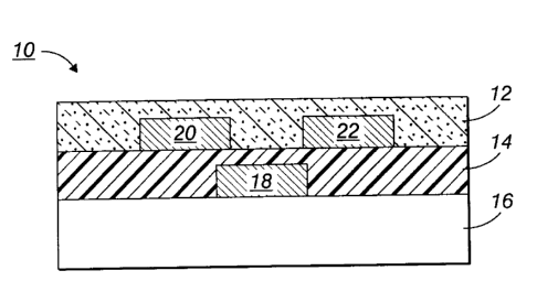
[0054] In FIG. 1, there is schematically illustrated an OTFT configuration 10
comprised of a substrate 16, in contact therewith a metal contact 18 (gate
electrode)
and a layer of a gate dielectric layer 14 on top of which two metal contacts,
source
electrode 20 and drain electrode 22, are deposited. Over and between the metal
contacts 20 and 22 is an organic semiconductor layer 12 as illustrated herein.
100551 FIG. 2 schematically illustrates another OTFT configuration 30
comprised
of a substrate 36, a gate electrode 38, a source electrode 40 and a drain
electrode 42, a
gate dielectric layer 34, and an organic semiconductor layer 32.
[0056] FIG. 3 schematically illustrates a further OTFT configuration 50
comprised
of a heavily n-doped silicon wafer 56 which acts as both a substrate and a
gate
electrode, a thermally grown silicon oxide gate dielectric layer 54, and an
organic
semiconductor layer 52, on top of which are deposited a source electrode 60
and a
drain electrode 62.
22
CA 02529245 2005-12-07
[0057] FIG. 4 schematically illustrates an additional OTFT configuration 70
comprised of substrate 76, a gate electrode 78, a source electrode 80, a drain
electrode
82, an organic semiconductor layer 72, and a gate dielectric layer 74.
[00581 The composition and formation of the semiconductor layer are described
herein.
[00591 The semiconductor layer has a thickness ranging for example from about
10
nanometers to about 1 micrometer with a preferred thickness of from about 20
to
about 200 nanometers. The OTFT devices contain a semiconductor channel with a
width W and length L. The semiconductor channel width may be, for example,
from
about 1 micrometers to about 5 millimeters, with a specific channel width
being about
micrometers to about 1 millimeter. The semiconductor channel length may be,
for
example, from about 1 micrometer to about 1 millimeter with a more specific
channel
length being from about 5 micrometers to about 100 micrometers.
[0060] The substrate may be composed of for instance silicon, glass plate,
plastic
film or sheet. For structurally flexible devices, a plastic substrate, such as
for example
polyester, polycarbonate, polyimide sheets and the like may be preferred. The
thickness of the substrate may be from about 10 micrometers to over about 10
millimeters with an exemplary thickness being from about 50 to about 100
micrometers, especially for a flexible plastic substrate and from about 1 to
about 10
millimeters for a rigid substrate such as glass plate or silicon wafer.
100611 The gate electrode can be a thin metal film, a conducting polymer film,
a
conducting film made from conducting ink or paste, or the substrate itself can
be the
gate electrode, for example heavily doped silicon. Examples of gate electrode
materials include but are not restricted to aluminum, gold, chromium, indium
tin
oxide, conducting polymers such as polystyrene sulfonate-doped poly(3,4-
ethylenedioxythiophene) (PSS-PEDOT), conducting ink/paste comprised of carbon
black/graphite or colloidal silver dispersion in polymer binders, such as
ELECTRODAGTM available from Acheson Colloids Company. The gate electrode
layer can be prepared by vacuum evaporation, sputtering of metals or
conductive
23
CA 02529245 2005-12-07
metal oxides, coating from conducting polymer solutions or conducting inks by
spin
coating, casting or printing. The thickness of the gate electrode layer ranges
for
example from about 10 to about 200 nanometers for metal films and in the range
of
about 1 to about 10 micrometers for polymer conductors.
100621 The source and drain electrode layers can be fabricated from materials
which provide a low resistance ohmic contact to the semiconductor layer.
Typical
materials suitable for use as source and drain electrodes include those of the
gate
electrode materials such as gold, nickel, aluminum, platinum, conducting
polymers
and conducting inks. Typical thicknesses of source and drain electrodes are
about, for
example, from about 40 nanometers to about 10 micrometers with the more
specific
thickness being about 100 to about 400 nanometers.
[0063] The gate dielectric layer generally can be an inorganic material film
or an
organic polymer film. Illustrative examples of inorganic materials suitable as
the gate
dielectric layer include silicon oxide, silicon nitride, aluminum oxide,
barium titanate,
barium zirconium titanate and the like; illustrative examples of organic
polymers for
the gate dielectric layer include polyesters, polycarbonates, poly(vinyl
phenol),
polyimides, polystyrene, poly(methacrylate)s, poly(acrylate)s, epoxy resin and
the
like. The thickness of the gate dielectric layer is, for example from about 10
nanometers to about 500 nanometers depending on the dielectric constant of the
dielectric material used. An exemplary thickness of the gate dielectric layer
is from
about 100 nanometers to about 500 nanometers. The gate dielectric layer may
have a
conductivity that is for example less than about 10-12 S/cm.
100641 The gate dielectric layer, the gate electrode, the semiconductor layer,
the
source electrode, and the drain electrode are formed in any sequence with in
embodiments the gate electrode and the semiconductor layer both contacting the
gate
dielectric layer, and the source electrode and the drain electrode both
contacting the
semiconductor layer. The phrase "in any sequence" includes sequential and
simultaneous formation. For example, the source electrode and the drain
electrode can
be formed simultaneously or sequentially. The composition, fabrication, and
24
CA 02529245 2005-12-07
operation of field effect transistors are described in Bao et al., US Patent
6,107,117,
the disclosure of which is totally incorporated herein by reference.
[0065] For a p-channel OTFT, the source electrode is grounded and a bias
voltage
of generally, for example, about 0 volt to about -80 volts is applied to the
drain
electrode to collect the charge carriers transported across the semiconductor
channel
when a voltage of generally about +20 volts to about -80 volts is applied to
the gate
electrode.
[0066] The semiconductor layer comprising the Compound in an OTFT device
generally exhibit a field-effect mobility of greater than for example about
10"3 cm2/Vs
(square centimeter per Volt per second), and an on/off ratio of greater than
for
example about 103. On/off ratio refers to the ratio of the source-drain
current when
the transistor is on to the source-drain current when the transistor is off.
[0067] The invention will now be described in detail with respect to specific
exemplary embodiments thereof, it being understood that these examples are
intended
to be illustrative only and the invention is not intended to be limited to the
materials,
conditions, or process parameters recited herein. All percentages and parts
are by
weight unless otherwise indicated. As used herein, room temperature refers to
a
temperature ranging for example from about 20 to about 25 C.
[0068] Example 1
[0069] (a) Synthesis ofpoly(5,11-dioctylindolo[3,2-bJcarbazole):
[0070] A solution of 5,11-dioctylindolo[3,2-b]carbazole (0.481 g, 1.0 mmol) in
chlorobenzene (10 mL) was added dropwise to a stirring mixture of FeC13 (0.681
g,
4.2 mmol) and chlorobenzene (20 mL) in a 100 mL flask at 0 C under an argon
atmosphere. The solution became dark blue immediately upon addition. After
stirring
for 48 h at room temperature, the reaction mixture was poured into methanol
(200
mL). The precipitated solid product was washed with water and methanol. After
washing, the product was suspended in dichloromethane (100 mL) with stirring
while
aqueous ammonia solution (30 %, 20 mL) was added. After stirring for 12 h, the
mixture was added to methanol. The solid product was collected and subject to
CA 02529245 2005-12-07
Soxhlet extraction, first with methanol for 24 h and then with heptane for
another 24
h. The remaining solid product was isolated by Soxhlet extraction with
refluxing
chlorobenzene. The resulting chlorobenzene solution was concentrated and then
added
to 100 mL of stirring methanol to precipitate the product. The solid product
was dried
under a reduced pressure overnight. Yield: 0.38 g.
[0071] (b) OTFTfabrication and evaluation.
[0072] A top-contact thin film transistor configuration as schematically
illustrated,
for example, in FIG. 3 was selected as our test device structure. The test
device was
built on an n-doped silicon wafer with a thermally grown silicon oxide layer
with a
thickness of about 110 nanometers thereon, and had a capacitance of about 30
nF/cm2
(nanofarads/square centimeter), as measured with a capacitor meter. The wafer
functioned as the gate electrode while the silicon oxide layer acted as the
gate
dielectric. The silicon wafer was first cleaned with isopropanol, argon
plasma,
isopropanol and air dried, and then immersed in a 0.1 M solution of
octyltrichlorosilane (OTS-8) in toluene at 60 C for 20 min. Subsequently, the
wafer
was washed with toluene, isopropanol and air-dried. A solution of poly(5,11-
dioctylindolo[3,2-b]carbazole) dissolved in dichlorobenzene (0.3 percent by
weight)
was first filtered through a 1.0 micrometer syringe filter, and then spin-
coated on the
OTS-8-treated silicon wafer at 1000 rpm for 120 seconds at room temperature.
This
resulted in the formation of a semiconductor layer with a thickness of 20-50
nanometers on the silicon wafer, which was then dried in a vacuum oven at 80
C for
5-10 h. Subsequently, gold source and drain electrodes of about 50 nanometers
in
thickness were deposited on top of the semiconductor layer by vacuum
deposition
through a shadow mask with various channel lengths and widths, thus creating a
series
of transistors of various dimensions.
[0073] The evaluation of transistor performance was accomplished in a black
box
(that is, a closed box which excluded ambient light) at ambient conditions
using a
Keithley 4200 SCS semiconductor characterization system. The carrier mobility,
,
was calculated from the data in the saturated regime (gate voltage, VG <
source-drain
voltage, VSD) according to equation (1)
26
CA 02529245 2005-12-07
IsD = C; (W/2L) (VC-VT)2 (1)
where ISD is the drain current at the saturated regime, W and L are,
respectively, the
semiconductor channel width and length, C; is the capacitance per unit area of
the gate
dielectric layer, and VG and VT are, respectively, the gate voltage and
threshold
voltage. VT of the device was determined from the relationship between the
square
root of IsD at the saturated regime and VG of the device by extrapolating the
measured
data to IsD = 0.
[0074] The transfer and output characteristics of the devices showed that the
Compound was a p-type semiconductor. Using transistors with a dimension of W =
5,000 m and L = 90 m, the following average properties from at least five
transistors were obtained:
Mobility: 2.1-2.8 x 10"3 cm2/Vs
On/off ratio: 104 _ 105.
[0075] Example 2
100761 (a) Synthesis of poly(5,11-bis(4-octylphenyl)indolo[3,2-bJcarbazole):
[0077] A solution of 5,11-bis(4-octylphenyl)indolo[3,2-b]carbazole (0.50 g,
0.79
mmol) in chlorobenzene (10 mL) was added dropwise to a stirring mixture of
FeCl3
(0.58 g, 3.56 mmol) and chlorobenzene (10 mL) in a 100 mL flask at room
temperature under an argon atmosphere. The resulting mixture was stirred at 50
C for
48 h and then poured into a stirring methanol (200 mL). The precipitated solid
product
was washed with water and methanol, and then suspended in dichloromethane (100
mL) while aqueous ammonia solution (30 %, 20 mL) was added. The resulting
mixture was stirred for 12 h and then added to 100 mL of stirring methanol.
The solid
product was collected and subjected to Soxhlet extraction, first with methanol
for 24 h
and then with heptane for 24 h. The remaining insoluble solid product was
isolated by
Soxhlet extraction with refluxing chlorobenzene. The resulting chlorobenzene
solution
27
CA 02529245 2005-12-07
was concentrated and then added to a stirring methanol (100 mL) to precipitate
the
product. The solid product was dried under a reduced pressure overnight.
Yield: 0.30
g=
[0078) (b) OTFT device fabrication and evaluation.
[0079] OTFT devices using poly(5,11-bis(4-octylphenyl)indolo[3,2-b]carbazole)
as
the semiconductor were fabricated and characterized in accordance with the
procedures of Example 1. Using transistors with a dimension of W = 5,000 m
and L
= 90 m, the following average properties from at least five transistors were
obtained:
Mobility: 1.3-1.8 x 10'3 cm2/Vs
On/off ratio: 104 _ 105.
[0080] The mobility and current on/off ratio achieved by embodiments of the
present thin film transistor devices are useful for various applications in
electronics
such as for example electronic paper.
28