Note: Descriptions are shown in the official language in which they were submitted.
CA 02529397 2005-12-14
WO 2005/002873 PCT/AU2004/000917
- 1 -
A METHOD OF FORMING A REFLECTIVE DEVICE
The present invention claims priority of Australian
provisional patent application 2003903501, the disclosure
of which is incorporated herein by reference.
Field of the Invention
The present invention relates to a reflective device.
When reflective devices made in accordance with
embodiments of the invention are illuminated by a light
source, they generate one or more images which are
observable within particular ranges of viewing angles
around the device. Devices of embodiments of the
invention may be used in a number of different
applications, and have particular application as an anti-
forgery security device on ID documents such as drivers
licenses, credit cards, visas, passports and other
valuable documents where secure identification of
individuals is required in a way which is resistant to
counterfeiting by printing, photocopying and computer
scanning techniques.
Embodiments of the invention also have particular
application as a low cost anti-counterfeiting device for
the protection of banknotes, cheques, credit cards and
other financial transaction documents such as share
certificates.
Background Art
It is to be understood that, if any prior art publication
is referred to herein, such reference does not constitute
an admission that the publication forms a part of the
common general knowledge in the art, in Australia or any
other country.
CA 02529397 2005-12-14
WO 2005/002873 PCT/AU2004/000917
- 2 -
The new series of American Express US dollar travellers
cheques, first issued in 1997, employed as an anti-
counterfeiting feature a diffraction grating foil image of
the American Express Centurion logo. When illuminated by
a light source and the diffraction grating foil device is
observed from different viewing angles, the Centurion
image appears to switch to an American Express box logo
image. This optical variability of the device ensures
that it is impossible to copy by normal photocopier or
camera techniques.
Diffraction grating devices which exhibit this variable
optical behaviour are referred to as optically variable
devices (OVDs) and their use as an anti-counterfeiting
measure to protect valuable documents is continuing to
grow. Examples of particular proprietary optically
variable devices and applications to date include the
EXELGRAM~ device used to protect the new series of
Hungarian banknotes, American Express US dollar and Euro
travellers cheques and the Ukrainian visa, and the
KINEGRAMTM device used to protect the current series of
Swiss banknotes and low denomination Euro banknotes. The
EXELGRAMTM device is described in US patent numbers
5,825,547 and 6,088,161 while the KINEGR.AM~ device is
described in European patents EP 330,738 and EP 105099.
The KINEGRAMTM and EXELGRAM~ devices are examples of foil
based diffractive structures that have proven to be highly
effective deterrents to the counterfeiting of official
documents. This class of optically diffractive
anti-counterfeiting devices also includes the PIXELGRAM~
device that is described in European patent number EP 0
490 923 B1 and US patent number 5,428,479. PIXELGR.AMT''z
devices are manufactured by producing a counterpart
diffractive structure wherein the greyness values of each
pixel of an optically invariable image are mapped to
corresponding small diffractive pixel regions on the
CA 02529397 2005-12-14
WO 2005/002873 PCT/AU2004/000917
- 3 -
PIXELGRAM~ device.
An alternative technique for producing an OVD is to use a
micro mirror array structure for the direct printing of an
optically variable device without the use of hot stamping
foil. The use of micro mirror arrays for the direct
printing of optically variable images is described in
International Patent Application No. PCT/AU02/00551
entitled "An Optical Device and Methods of Manufacture".
In spite of their industrial effectiveness, these foil
based diffractive and reflective optically variable
devices have a particular deficiency for low volume
applications and for one-off applications requiring secure
identification of the images of individuals such as for
the case of passport or drivers license photographs or
identification (ID) card images.
At the present time techniques for protecting an
individual portrait image on an ID document using a
diffractive OVD include the origination of an OVD image
specific to that individual, covering the photograph of
the person with a transparent OVD laminate or film or
including a standard OVD image on the ID document in an
adjacent area of the document. In the first case the
process is extremely expensive and time consuming because
of the need to produce a new OVD origination for each
individual and then produce a hot stamping foil image by
embossing techniques. As the cost of OVD originations for
security purposes varies from US$5,000 to US$50,000,
depending on the technology type and level of security
required, the use of individual specific OVD originations
for ID applications is not viable for cost reasons alone.
Generally speaking, the high cost of OVD originations
means that this type of anti-counterfeiting technology is
only suited to mass production applications where the cost
CA 02529397 2005-12-14
WO 2005/002873 PCT/AU2004/000917
- 4 -
of the origination can be amortized over a large
production run of identical hot stamping foils. The use
of transparent OVD overlay films and the use of a generic
OVD image are methods currently employed for amortizing
the OVD origination cost over a foil production run for ID
applications. However, in these cases the transparent
overlay film or OVD image is not specific to the
individual and therefore there is a risk that a substitute
or counterfeit document could be produced by peeling back
the transparent film and replacing the original
photographic image by a substitute image to allow a
different individual the use of the ID document.
Another technique which has been developed for security of
applications is known as Screen Angle Modulation, "SAM",
or its micro-equivalent, "~-SAM", is described in detail
in US patent number 5,374,976 and by Sybrand Spannenberg
in Chapter 8 of the book "Optical Document Security,
Second Edition" (Editor: Rudolph L. van Renesse, Artech
House, London, 1998, pages 169-199). In this technique,
latent images are created within a pattern of periodically
arranged, miniature short-line segments by modulating
their angles relative to each other, either continuously
or in a clipped fashion. While the pattern appears as a
uniformly intermediate colour or grey-scale when viewed
macroscopically, a latent image is observed when it is
overlaid with an identical, non-modulated pattern on a
transparent substrate.
As noted above, these techniques involve overlaying a
modulated array with the corresponding unmodulated array,
or vice versa, in order to reveal the latent image.
The modulated and unmodulated arrays of this technique are
usually produced by printing techniques. For this reason,
this technique is not as secure as a diffractive OVD
because it is more easily reverse engineered than the much
CA 02529397 2005-12-14
WO 2005/002873 PCT/AU2004/000917
- 5 -
smaller scale microstructures of a diffractive OVD.
It would be desirable to provide an alternative method of
producing an authentication device.
Summary of the Invention
In a first broad aspect, the invention relates to a method
of forming a reflective device which generates an
optically variable image which varies according to the
angle of observation, the method comprising the steps of:
providing a' primary pattern which encodes a
latent image, the primary pattern having a plurality of
image elements; and
providing a corresponding secondary pattern which
will decode the primary pattern to allow the latent image
to be observed when the primary and secondary patterns are
in at least one registration, wherein the secondary
pattern is provided by a micro mirror array (1~2A) having a
plurality of each of at least two different types of micro
mirror elements,
wherein the primary pattern is provided such that
predetermined image elements of the primary pattern render
reflection effects from predetermined micro mirror
elements of the 1~2A optically ineffective at least at one
observation angle when the reflective device is
illuminated with a light source to thereby enable the
latent image to be observed.
In some embodiments, the primary pattern is provided by
being overlaid on the secondary pattern.
In still further embodiments, the primary pattern is
provided by being printed in register with the secondary
pattern.
In other embodiments, the primary pattern is provided by
CA 02529397 2005-12-14
WO 2005/002873 PCT/AU2004/000917
- 6 -
rendering the micro mirror elements optically ineffective.
Depending on the embodiment micro mirror elements may be
rendered optically ineffective by physically removing them
(e.g. laser ablation), or by reducing its ability to
reflect so that it does not reflect strongly.
The two types of micro mirror elements will typically be
provided in a regular pattern. Typically, the regular
pattern is provided by arranging at least two types of
micro mirror elements into either pixellated or track-like
pattern. An example of pixellated pattern is a
checkerboard pattern, where a plurality of two different
types of micro mirror elements are arranged in a
rectangular array so that they alternate in each of the
horizontal and vertical axes.
Herein, the micro mirror elements are rendered "optically
ineffective" in the sense that reflection effects from
these pre-selected elements are either eliminated or
greatly reduced in terms of the intensity of the reflected
light from these element relative to the other micro
mirror elements.
The method may further include the steps of producing the
micro mirror elements by:
I) producing a variable transparency photomask
by electron beam lithography and wet or dry etching
techniques;
II) using the photomask in an optical contact
printing or projection system to create a surface relief
pattern of two types of interlaced micro mirror structures
arranged in a desired pattern;
III) producing a printing plate embossing die by
the use of electroplating techniques applied to the
created micro mirror array structure; and
IV) applying ink to a paper or polymer
substrate using screen printing techniques and embossing
CA 02529397 2005-12-14
WO 2005/002873 PCT/AU2004/000917
the micro mirror array structure into the inked substrate.
In an embodiment, where the primary pattern is provided by
being overlaid on the secondary pattern, the primary
pattern is provided upon a transparent substrate, and the
secondary pattern is provided in the form of an embossed
substrate and the method involves aligning the primary
pattern with the OVD secondary pattern in correct register
such that the image elements of the latent image encoded
in the primary pattern render micro mirror elements of the
secondary pattern optically ineffective.
In a further aspect of the invention, the micro mirror
elements are additionally encoded to produce a secure
generic optical variability effect and the overlay ID
screen or primary pattern is encoded with image
information specific to a particular individual in such a
way that the image of the individual disappears upon
delamination of the film from the document. This
embodiment greatly enhances ID security over present OVD
lamination techniques because neither the OVD substrate
nor the encoded overlay screen are open to modification
using current photographic or printing techniques.
In an embodiment of the invention where the primary
pattern is printed, the primary pattern is directly
printed on top of the previously embossed printed generic
OVD micro mirror array (l~ff~IA) substrate thereby providing
increased security by preventing reverse engineering of
the 1~IA and overlay screen interface by delamination.
In a further alternative embodiment of the invention where
the micro mirror elements are altered, the primary pattern
is directly incorporated into the OVD 1~IA by laser heating
of the embossed I~IA so as to destroy particular micro
mirror elements at selected locations within the OVD area
determined by the primary pattern data file. This
CA 02529397 2005-12-14
WO 2005/002873 PCT/AU2004/000917
_ g _
implementation of the invention improves both the
durability of the ID image over the previous alternative
direct printing method because there is no possibility of
erasing the encoded image information from the surface of
the emboss printed MMA.
A number of techniques may be used to produce appropriate
primary and secondary patterns. These techniques share
the feature of producing a modulated array of image
elements which encodes a latent image (the "primary"
pattern) and a corresponding unmodulated array of image
elements (the "secondary" pattern) which will decode the
latent image when in register with the unmodulated array.
As both the modulated and unmodulated arrays are divided
into a plurality of discrete image elements, it is
appropriate to refer to the modulated and unmodulated
arrays as "digital" images. Accordingly, techniques of
this type are collectively referred to herein as
"modulated digital images" (MDI). Examples of suitable
MDI techniques include SAM, ~-SAM, as well as PHASEGRAM,
BINAGR.AM, and TONAGRAM.
PHASEGR.AMS are described in International patent
application no. 2003905861 entitled "Method of Encoding a
Latent Image", filed 24 Oct 2003 for which a PCT
application was filed on 7 July 2004 entitled "Method of
encoding a latent image". In this technique, an image is
encoded within a locally periodic pattern by selectively
modulating the periodicity of the pattern. When overlaid
upon or overlaid with the original pattern on a
transparent substrate, the latent image or various shades
of its negative becomes visible to an observer depending
on the exactness of the registration.
BINAGRAMS are described in International Patent
application no. PCT/AU2004/00746 entitled: "Method of
Encoding a Latent Image", filed 4 .Tune 2004. In this
CA 02529397 2005-12-14
WO 2005/002873 PCT/AU2004/000917
_ g _
technique, an image is divided into pairs of adjacent or
nearby pixels, which may be locally periodic or not. One
of the pixels in each pair is then selectively modulated
to the complementary grey-scale or colour characteristic.
When overlaid upon or overlaid with an equivalent
non-modulated pattern on a transparent substrate, the
latent image or its negative becomes visible depending on
the extent of registration.
The primary pattern, as defined in this specification,
will typically be a modulated version of the secondary
pattern. The primary pattern encodes or incorporates a
latent image or images; these are revealed only when the
primary pattern is overlaid upon the corresponding
secondary pattern (in the form of an OVD in embodiments of
the present invention). The image elements employed in
the primary pattern are typically pixels (i.e. the
smallest available picture element). Typically, the
primary pattern will be rectangular and hence its image
elements will be organised in a rectangular array.
However, the image elements may be arranged in other ways.
Image elements will typically be arrayed in a periodic
fashion, such as alternating down one column or one row,
since this allows the secondary pattern to be most easily
registered with the primary pattern in overlay. However
random or scrambled arrangements of image elements may be
used.
In this specification, the term "secondary pattern" is
used in two contexts, either describing a pattern which
will decode a primary pattern when overlying or overlaid
by the primary pattern (depending on the nature of the
primary pattern) or to describe such a secondary pattern
as applied to a substrate. When the secondary pattern is
applied to form an array of micro mirror elements (a micro
mirror array (I~IA)) as described in this specification,
the secondary pattern consists of micro mirror elements
CA 02529397 2005-12-14
WO 2005/002873 PCT/AU2004/000917
- 10 -
which correspond to the image elements which either
effectively reflect light ("on" micro mirror elements) or
reflect light ineffectively ("off" micro mirror elements)
at a particular angle of observation. These micro mirror
elements are arrayed in the pattern of the secondary
pattern which also corresponds to the primary pattern
employed to encode the latent image. The physical
dimensions of the micro mirror elements in the physical
secondary pattern are, moreover, substantially identical
to those of the image elements of an secondary pattern
image which corresponds to the primary pattern employed.
The "on" and "off" micro mirror elements are arrayed in
such a way that when illuminated with a light source, they
contrast image elements within the primary pattern that
reveal the latent image, or an image related thereto. The
optical variability of the device is achieved when the
angle of view is changed to other specific angles of view
and all of the "off" micro mirror element convert to "on"
pixels and vice versa. To achieve the required contrast
it is necessary that all of the "on" micro mirror elements
at any specific angle of observation must reflect light,
while all of the "off" pixels do not reflect light at this
angle.
The secondary pattern will typically be a regular array of
"on" and "off" micro mirror elements. For example, a
secondary pattern may be "track-like", that is, a
rectangular array consisting of a plurality of vertical
lines of "on" micro mirror elements, each line being 1
micro mirror element wide and separated by identically
wide vertical lines of "off" micro mirror elements.
Another typical secondary pattern may be a checkerboard of
"on" and "off" micro mirror elements. Random and
scrambled arrays may, however, also be used, so long as
the "on" micro mirror elements in the secondary pattern
are capable, when in correct register, of contrasting all
of the image elements in the primary pattern which reveal
CA 02529397 2005-12-14
WO 2005/002873 PCT/AU2004/000917
- 11 -
the latent image.
The secondary pattern is also referred to in the present
specification as the "background OVD" or "background MMA".
Another technique which may be used to create a primary
pattern from a secondary pattern is known as TONAGRAM and
described in Australian Provisional Patent application
2004900187 entitled "Method of Concealing an Image" filed
17 January 2004.
In this technique, an MDI, such as a BINAGRAM or a
PHASEGRAM is mathematically combined with an overt image,
such as a photographic portrait, to thereby render a
primary pattern which contains both the overt image and
one or more concealed latent images. V~Ihen overlaid with
the corresponding secondary pattern, the latent images are
revealed. In the same way, a secondary pattern consisting
of a micro mirror array of the type described in this
application may be overlaid with a printed TONAGRAM
primary pattern, thereby rendering an OVD containing an
overt image which is visible at all angles of observation
and which contains one or more latent images which are
visible only at selected angles of observation.
Alternatively, a blank canvas micro mirror array which
serves as the secondary pattern may be rendered optically
ineffective in selected areas according to a TONAGRAM
algorithm. An OVD containing an overt image which is
visible at all angles of observation and which contains
one or more latent images which are visible only at
selected angles of observation is thereby created.
The invention also extends to a reflective device, such as
a reflective authentication device or a novelty item
produced by the foregoing method as well as to documents
or instruments incorporating a reflective device.
CA 02529397 2005-12-14
WO 2005/002873 PCT/AU2004/000917
- 12 -
In another broad aspect, the invention relates to a
reflective device which generates an optically variable
image which varies according to the angle of observation,
the reflective device comprising:
a primary pattern which encodes a latent image,
the primary pattern having a plurality of image elements;
and
a corresponding secondary pattern which will
decode the primary pattern to allow the latent image to be
observed when the primary and secondary patterns are in at
least one registration, wherein the secondary pattern is
provided by a micro mirror array (MMA) comprising a
plurality of each of at least two different types of micro
mirror elements, and
wherein the primary pattern is provided such that
the predetermined image elements of the primary pattern
render reflection effects from predetermined micro mirror
elements of the MMA optically ineffective at least at one
observation angle when the authentication device is
illuminated with a light source to thereby enable the
latent image to be observed.
As outlined above, a micro mirror array, patterned in the
arrangement of a MDI secondary pattern by using two types
of micro mirror elements in place of a printed MDI
pattern, can be masked by the corresponding MDI primary
pattern to generate the MDI latent image in the form of a
unique, OVD effect. The resulting hybrid OVD-MDI,
referred to here as an MM-VOID (or "Micro Mirror Variable
Optical Identification Device"), displays optically
variable properties which are difficult to counterfeit,
but is nevertheless easily customised because the primary
pattern can be readily printed and the OVD-based secondary
pattern can be mass produced in a generic form.
Embodiments of the present invention therefore provide a
more general and useful approach to the protection of
CA 02529397 2005-12-14
WO 2005/002873 PCT/AU2004/000917
- 13 -
images on security documents by separating the optically
variable and identification aspects of the image in such
way that the two aspects can be manufactured separately
and recombined in an overlay manner. In other words, the
present invention incorporates the OVD protection into a
generic type of reflecting OVD micro mirror array (I~IA)
which is emboss printed onto a document to be protected
and this 1~IA is then overlaid either with a transparent
film containing the encoded ID information or printed in
register with the ID information pattern. The combination
of these two effects reveals the encoded image as a latent
image displaying OVD effects.
Furthermore, in embodiments of the invention the use of a
printing or embossing technique to produce the NIA in the
preferred embodiment is firstly very cost-effective and
secondly allows the N~iA to be produced locally. The
improves security as it is not necessary to transport
material incorporating the N~iA.
Further features of the invention will become apparent
from the following description of preferred embodiments of
the invention.
Brief Description of the Drawings
The preferred embodiments will be described with reference
to the accompanying drawing in which:
Figure 1 depicts a particular arrangement of the
background NIA or secondary pattern;
Figure 2 shows another arrangement of the
background NIA or secondary pattern;
Figure 3 shows an example of a primary Pattern
corresponding to a particular ID application;
Figure 4 shows the primary pattern of Figure 3
added to the background N~iA (secondary pattern)
CA 02529397 2005-12-14
WO 2005/002873 PCT/AU2004/000917
- 14 -
corresponding to Figure 2;
Figure 5 shows the image generated by the
overlaid primary and secondary pattern of Figure 4
observed at a particular angle of view;
Figure 6 shows the image generated by the
overlaid primary and secondary patterns of Figure 4
observed at another particular angle of view;
Figure 7 shows an example of a primary pattern;
Figure 8 shows the primary pattern of Figure 7
added to the background OVD NIA (secondary pattern)
corresponding to Figure 1;
Figure 9 shows the image generated by the
overlaid primary and secondary patterns of Figure 8
observed at another particular angle of view;
Figure 10 shows the image generated by the
overlaid primary and secondary screens of Figure 8
observed at a particular angle of view; and
Figure 11 shows a micrograph of a small section
o f a Na2A .
Further Description of the Drawings
Preferred embodiments of the invention will initially be
described in relation to the visual effects which can be
produced by combining an 1~I primary pattern with a
secondary pattern in the form of a micro mirror array.
Following this description is a description of some
possible techniques for constructing reflective
authentication devices.
Figure 1 is an illustrative example of a background l~iA
(or secondary pattern). In Figure 1, the pixel areas
having different shades represent two different types of
reflecting micro mirror elements as best seen in enlarged
section 10. For convenience these shades will be referred
to as red (the lighter shade) and blue (the darker shade)
pixel areas. Typical dimensions of the micro mirror pixel
CA 02529397 2005-12-14
WO 2005/002873 PCT/AU2004/000917
- 15 -
areas would be 30 microns X 30 microns or 60 microns X 60
microns. For some applications the dimensions of the
pixels may be smaller or larger than these figures
depending on the image resolution required for the
application.
Figure 2 shows another arrangement of the background OVD
microstructure or secondary pattern. In Figure 2 the red
and blue strip or track areas represent two different
types of NIA as best seen in enlarged section 10.
Typically the width of the tracks would be 30 microns or
60 microns. For some applications the width of the strips
or tracks may be smaller or larger than these figures
depending on the image resolution required for the
application. The length of the tracks is a function of
the image area required for the application and may be 20
mm or longer. The maximum depth is typically 20mm as
illustrated by the micrograph of Figure 11, where the
micro mirror elements have two different slopes.
The choice of 1~I secondary pattern will depend on the
embodiment.
Figure 3 shows a primary pattern of a first preferred
embodiment into which an image has been encoded by
modulation of the secondary pattern shown in Figure 2.
The method of forming the modulated digital image (1~I) is
that of a BINAGR.AM.
In a BINAGRAM, the primary pattern is typically formed
from an original image. In an example where the original
image is a photograph, this original image is then
dithered into image elements which have one of a set of
primary visual characteristics. The primary visual
characteristics will be grey-scale values or hues
depending on the embodiment. The original elements are
then paired, typically with a neighbouring image element.
CA 02529397 2005-12-14
WO 2005/002873 PCT/AU2004/000917
- 16 -
In the example of a preferred embodiment, the image
elements are paired such that when overlaid with the
corresponding secondary pattern, one element in each pair
will correspond to the red track and one will correspond
to the blue track. The image elements are then
transformed. In a typical transformation, one pixel in
each pair will take the average value of the visual
characteristics of the pair and the other pixel is
allocated a complementary visual characteristic. Thus,
one pixel in each pair acts to carry information from the
original image while the other disguises the information.
An alternative method of forming the primary pattern is to
use a computer graphics program such as Adobe Photoshop to
produce both positive tone and negative tone versions of
an original image such as a portrait image. The positive
tone and negative tone images can then be combined into a
primary pattern by; firstly filtering the positive tone
image with the "on" pixels of the secondary screen ( that
is removing all pixels from the positive tone image
corresponding to the positions of the "off" pixels on the
secondary screen) and then converting the resultant
filtered positive tone image to a bitmap version by using
the dithering option within the computer graphics program;
secondly applying the reverse procedure to the negative
tone image by filtering the negative tone image with the
"off" pixels of the secondary pattern (that is removing
all pixels from the negative tone image corresponding to
the positions of the "on" pixels on the secondary screen)
and then converting the resultant filtered negative tone
image to a bitmap version by using the dithering option
within the computer graphics program; and finally
overlaying the filtered and dithered versions of both the
negative tone and positive tone images to obtain the
resultant primary pattern version of the input portrait
image.
CA 02529397 2005-12-14
WO 2005/002873 PCT/AU2004/000917
- 17 -
Figure 4 shows a simple addition of the primary image in
Figure 3 to the secondary pattern in Figure 2 where the
black pixels have been rendered optically ineffective by
being erased, the dark grey pixels indicate the original
blue pixels which have been retained, and the light grey
pixels indicate the original red pixels which have been
retained as can best be seen by reference to enlarged
section 40.
Figure 5 depicts the image seen by an observer at one
particular range of viewing angles with the red OVD tracks
"on" and therefore displayed as white for clarity; the
blue pixels are "off" at this angle and therefore appear
black as best seen in enlarged section 50. Figure 6
depicts the image seen by an observer at another
particular range of viewing angles with the blue tracks
"on" and therefore displayed as white for clarity; the red
pixels are "off" at this angle and therefore appear black
as best seen in enlarged section 60.
Figures 5 and 6 demonstrate that an optically variable
effect can be generated by printing techniques if the
background canvas is comprised of an OVD NIA consisting of
two groups of micro mirror elements (that is, the
secondary pattern). The OVD effect shown in these figures
corresponds to a switch of a portrait image from positive
tone to negative tone as the angle of view is changed.
This principle of using a background OVD canvas to convert
a printed image into optically variable form can be
extended to the case of two-channel OVD images. An
example of such a process is now described.
Figure 7 depicts a primary pattern consisting of a two-
channel image. In this case, the primary pattern is a
modulated form of the secondary pattern shown in Figure 1
and encodes two separate latent images. Enlarged portion
CA 02529397 2005-12-14
WO 2005/002873 PCT/AU2004/000917
- 18 -
70 shows a detail of where the two faces of the images
overlap.
A primary pattern corresponding to a two channel image can
also be prepared using a computer graphics program such as
Adobe Photoshop. Two original input images can be
combined into a primary pattern by; firstly filtering the
first image with the "on" pixels of the secondary screen
(that is removing all pixels from the first image
corresponding to the positions of the "off" pixels on the
secondary screen) and then converting the resultant first
image to a bitmap version by using the dithering option
within the computer graphics program; secondly applying
the reverse procedure to the second image by filtering the
second image with the "off" pixels of the secondary
pattern (that is removing all pixels from the second image
corresponding to the positions of the "on" pixels on the
secondary screen)and then converting the resultant
filtered second image to a bitmap version by using the
dithering option within the computer graphics program; and
finally overlaying the filtered and dithered versions of
both the first and second images to obtain the resultant
two channel primary pattern corresponding to the two input
images.
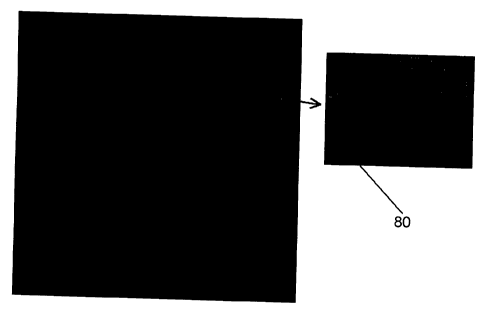
Figure 8 illustrates an addition of Figure 7 and Figure 1
where the black pixels have been rendered optically
ineffective by being erased, the dark grey pixels indicate
the original blue pixels which have been retained, and the
light grey pixels indicate the original red pixels which
have been retained as best seen in enlarged portion 80.
Figure 9 depicts the image seen by an observer at one
particular range of viewing angles with the red OVD pixels
"on" and therefore displayed as white for better clarity;
the blue pixels are "off" at this angle and therefore
appear black as shown in enlarged portion 90.
CA 02529397 2005-12-14
WO 2005/002873 PCT/AU2004/000917
- 19 -
Figure 10 depicts the image seen by an observer at another
particular range of viewing angles with the blue tracks
"on" and therefore displayed as white for better clarity;
the red pixels are "off" at this angle and therefore
appear black as shown in enlarged portion 100.
Figures 9 and 10 confirm that a two channel optically
variable effect can also be generated by printing
techniques if the background canvas is comprised of an OVD
MMA consisting of two groups of micro mirror elements
(that is, the secondary pattern). The OVD effect shown in
these figures corresponds to a switch from one positive
tone portrait image to another positive tone portrait
image as the angle of view is changed.
The examples shown in Figures 1 to 10 are intended to
illustrate two particular embodiments of the new
invention. Many other embodiments of the invention are
possible and the generality of these applications makes
the invention particularly suited to the areas of identity
verification for ID documents and also for the
authentication of banknotes, cheques and other financial
transaction documents which suffer from a risk of
counterfeiting by printing, computer scanning, and colour
copying techniques.
A further embodiment of the invention can be realised by
recognising that the two channel mechanism described above
allows for the possibility of encoding data in an
individual manner by using bar code patterns for the
images in the two channels. The result will be in the
form of a micro mirror bar code with the first bar code
pattern able to be read by a laser at a first angle of
view and the second and different bar code pattern read at
a second angle of view. The security and integrity of the
data is ensured by a software correlation process
CA 02529397 2005-12-14
WO 2005/002873 PCT/AU2004/000917
- 20 -
involving the two bar code components. Writing of the
data is achieved by a printing process involving the
interlacing of the two bar codes on a reflecting micro
mirror background in the form of an interlacing of micro
mirror tracks of two different mirror angles.
The concepts described above can also be extended to
include the case of a two channel image where the image in
one channel is a generic image fixed at the time of
fabricating the secondary pattern microstructure. The
second channel image is then constructed by using a
computer graphics program to create a primary pattern that
can be individualised at the point of use of the device.
An example of this type of application would be a passport
application. In the case of an Australian passport the
generic image could be the Coat of Arms of Australia and
the second channel image would be a portrait image of the
passport holder and the device could be incorporated into
the data page of the passport. As the angle of view of
the data page is changed the image generated by the
authentication device would change from an image of the
passport holder to the Coat of Arms thereby securely
confirming that the passport holder is a citizen of
Australia.
One method of forming a reflective authentication device
in accordance with the invention involves the steps of:
I) Producing a variable transparency photomask
by electron beam lithography and wet or dry etching
techniques.
II) Using the photomask in an optical contact
printing or projection system to create a surface relief
pattern of two types of interlaced micro mirror structures
arranged in a pixellated (e. g. Figure 1) or track-like
(e. g. Figure 2) configuration.
III) Producing a printing plate embossing die by
the use of electroplating techniques applied to the
CA 02529397 2005-12-14
WO 2005/002873 PCT/AU2004/000917
- 21 -
created micro mirror array structure.
IV) Applying ink to a paper or polymer
substrate using screen printing techniques and embossing
the micro mirror structure into the inked substrate by
embossing techniques to produce an array of micro mirror
elements.
V) Encoding one or more images which will be
visible as the latent image (e. g. of a specific person,
and/or object, or design) into a pixellated or track based
primary pattern having a plurality of image elements which
correspond to the secondary pattern; and
VI) adding a physical representation of the
primary pattern on top of the micro mirror array
background OVD in such a manner that pre-selected areas of
the background microstructure are rendered optically
ineffective in the sense that reflection effects from
these pre-selected regions are either eliminated or
greatly reduced in terms of the intensity of the
reflected light from these regions. The position and area
of each pre-selected ineffective region being determined
from the primary pattern.
Typically where the secondary pattern is track-like, each
track has a width greater than 1 micron and it is typical
that at least one track is greater than 1 mm in length.
Where the secondary pattern is a pixellated array or micro
mirror element each micro mirror element typically has an
edge length greater than 1 micron.
Depending on the embodiment, within each micro mirror
element the micro mirror surfaces may be modulated or
varied in shape, curvature or slope.
It is preferred that the modulation of the micro mirror
surfaces within each micro mirror element is designed to
maximise the reflection efficiency of the reflected light
CA 02529397 2005-12-14
WO 2005/002873 PCT/AU2004/000917
- 22 -
from these elements at a particular distance from the
device by means of a focussing of the reflected light at
these distances. The modulation of the micro mirror
surfaces within each micro mirror element may be described
in terms of micro mirror surfaces shaped into a convex or
concave form.
In one preferred embodiment, the micro mirror slopes of
one of the two types of micro mirror elements are arranged
to lie at right angles to the slopes of the micro mirror
surfaces of a second group of micro mirror regions.
The primary pattern can be added in a number of different
ways.
One way is to overlay a transparent film printed with the
primary pattern file on top of the background 1~IA, the
printed regions of the transparent screen being made
opaque to reflected light by the printing process to
thereby render reflected light optically ineffective.
Alternatively, the primary pattern may be printed directly
on top of the background OVD NIA in order to make selected
regions of the reflective background opaque or only
partially transmitting to reflected light to thereby
render them optically ineffective.
A further alternative technique is to use the laser
ablation of selected micro mirror elements of the
background 1~IA in order to make these regions non-
reflecting or greatly reduced in the intensity of their
reflected light, the distribution of the ablated regions
being determined by the primary pattern.
The OVD I~IA can also be embossed into a transfer foil and
the transfer foil applied to the document to be protected
by a hot stamping process or as a foil based label and
CA 02529397 2005-12-14
WO 2005/002873 PCT/AU2004/000917
- 23 -
such label being adhesively attached to the document
requiring protection from counterfeiting.
Exemplary documents include a passport, visa, credit card,
drivers license, a social security card, a banknote,
cheque, share certificate or any other type of financial
transaction document to protect the document against
forgery or counterfeiting.
In addition to the BINAGRAM method for producing the
primary pattern set out above the primary pattern may be
produced according to the technique, known as "SAM" or "
SAM", as described in US patent number 5,374,976 and by
Sybrand Spannenberg in Chapter 8 of the book "Optical
Document Security, Second Edition" (Editor: Rudolph L. van
Renesse, Artech House, London, 1998, pages 169-199), or in
the technique known as PHASEGRAM (Australian Provisional
patent entitled "Method of Encoding a Latent Image",
Australian Provisional Patent number 2002952220 (23 Oct
2002).
In this technique, an image is encoded within a locally
periodic pattern by selectively modulating the periodicity
of the pattern. When overlaid upon or overlaid with the
original pattern on a transparent substrate, the latent
image or various shades of its negative becomes visible to
an observer depending on the exactness of the
registration.
The periodicity of the image is modulated by phase-
shifting image elements to create an encoded image. That
is, different displacements are applied to image elements
depending upon a value of a visual characteristic (e.g. a
grey-scale value or a hue). A PHASEGRAM embodiment will
typically utilise a secondary pattern where the micro-
mirror elements are arrayed in columns of alternating
types of micro-mirror elements N micro-mirror elements
CA 02529397 2005-12-14
WO 2005/002873 PCT/AU2004/000917
- 24 -
wide. This allows N+1 visual characteristic values to be
encoded.
A latent image (the image which it is desired to be able
to view) is formed by taking an original image and
separating it into image elements which only take one of
the set of allowable values of the visual characteristic.
The latent image is then related to a preliminary primary
pattern which has image elements corresponding to those of
the secondary pattern. The image elements of the primary
pattern are then displaced in accordance with their
relationship with the value of the visual characteristic
of the latent image elements with which they are related
to form a final primary pattern which encodes the latent
image.
Various different displacement schemes can be used. An
example, is one where there are M shades or hues and image
elements related to a first shade or hue are displaced by
one image element (e.g. a distance corresponding to the
width of a micro-mirror element), the second shade or hue
is displaced by two image elements etc. with the Mth shade
or hue displaced by M image elements.
Another technique which may be used to create a primary
pattern from a secondary pattern is known as TONAGRAM and
described in Australian Provisional Patent application
2004900187 entitled "Method of Concealing an Image" filed
17 January 2004, which is incorporated herein by
reference.
In this technique, an MDI, such as a BINAGR.AM or a
PHASEGRAM is mathematically combined with an overt image,
such as a photographic portrait, to thereby render a
primary pattern which contains both the overt image and
one or more concealed latent images. When overlaid with
the corresponding secondary pattern, the latent images are
CA 02529397 2005-12-14
WO 2005/002873 PCT/AU2004/000917
- 25 -
revealed. In the same way, a secondary pattern consisting
of a micro mirror array of the type described in this
application may be overlaid with a printed TONAGRAM
primary pattern, thereby rendering an OVD containing an
overt image which is visible at all angles of observation
and which contains one or more latent images which are
visible only at selected angles of observation.
Alternatively, a blank canvas micro mirror array which
serves as the secondary pattern may be rendered optically
ineffective in selected areas according to a TONAGRAM
algorithm. An OVD containing an overt image which is
visible at all angles of observation and which contains
one or more latent images which are visible only at
selected angles of observation is thereby created.
A further alternative two-channel technique may involve
encoding two separate but identical latent images which
are observable at two slightly offset observation angles,
the offset being chosen such that when observed by a human
observer at an appropriate distance from the image
surface, a stereoscopic effect allows the observer to
perceive a three-dimensional image.
Thus, in a further embodiment it is possible to create a
mask (e. g. a primary pattern) which encodes two identical
images in such a manner that they are observable at offset
observation angles when the mask overlays an appropriate
secondary pattern, such as the secondary patterns
disclosed herein.
In a two-channel case where the secondary pattern is shown
in Figure 1, the primary pattern may be produced by a
technique where a positive tone version of an original
image may fractured into a checkerboard pattern, and every
alternate cell of the checkerboard (e. g. every "black"
cell) is removed, and then a semi-transparent version of
the image remainder is created by binary dithering or
CA 02529397 2005-12-14
WO 2005/002873 PCT/AU2004/000917
- 26 -
sampling techniques and the resultant fractured binary
dithered version of the positive tone original image is
overlaid by a second checkerboard fractured binary
dithered image based on a negative tone image of the
subject where in this case every inverse fractured
checkerboard cell (e. g. every "white" cell)of the negative
tone original image is removed to allow these areas to be
occupied by the corresponding binary dithered ("black")
cells of the positive tone original image of the subject.
Various additional modifications will be apparent to
person skilled in the art. For example, the background
I~IA may also include optically variable effects that are
generic in nature and non-specific to the person, object
or design that is being authenticated by the reflective
device. Further, the l~iA of the device may also
incorporate extremely small scale images of size less than
60 microns in width and which can be used to provide a
higher degree of authentication or security by means of
microscopic examination of the I~iA.
One advantage of the current I~IA device over foil based
OVD devices is provided by the fact that there is no
requirement for hot stamping foil and this allows for much
lower costs for applications requiring high volume
production. This lower cost is achieved by having the 1~IA
embossing process arranged in line with the various
printing processes used to produce the particular
document.
Further, embodiments of the present invention also offer
much higher security over diffractive devices. This is
due, in part, to complexity of the unique production
processes required for the fabrication of the master I~IA
embossing/printing tools.
Reference may be made to International Patent Application
No. PCT/AU02/00551 for further details as to how to
construct an appropriate micro mirror array.
CA 02529397 2005-12-14
WO 2005/002873 PCT/AU2004/000917
- 27 -
Persons skilled in the art will appreciate that various
modifications can be made to the present invention without
departing from the scope of the invention. These and
other modifications will be apparent to those skilled in
the art.