Note: Descriptions are shown in the official language in which they were submitted.
CA 02529519 2005-12-07
Attorney Docket No. OS-1-206
LAMP HAVING FIXED FORWARD PHASE SWITCHING POWER SUPPLY
WITH TIME-BASED TRIGGERING
Background of the Invention
[0001] The present invention is directed to a power controller that supplies a
specified power to a load, and more particularly to a voltage converter for a
lamp that
converts line voltage to a voltage suitable for lamp operation.
[0002] Some loads, such as lamps, operate at a voltage lower than a line (or
mains) voltage of, for example, 120V or 220V, and for such loads a voltage
converter
that converts line voltage to a lower operating voltage must be provided. The
power
supplied to the load may be controlled with a phase-control clipping circuit
that includes
an RC circuit. Some of these loads operate most efficiently when the power is
constant
(or substantially so). However, line voltage variations are magnified by the
RC circuit
phase-control circuits due to their inherent properties (as will be explained
below). A
(more nearly) constant RMS load voltage from the phase-control circuit is
desirable.
[0003] A simple four-component RC phase-control clipping circuit demonstrates
a problem of conventional phase-control clipping circuits. The phase-
controlled clipping
circuit shown in Figure 1 has a capacitor 22, a diac 24, a triac 26 that is
triggered by the
diac 24, and resistor 28. The resistor 28 may be a potentiometer that sets a
resistance in
the circuit to control a phase at which the triac 26 fires.
CA 02529519 2005-12-07
[0004] In operation, a clipping circuit such as shown in Figure 1 has two
states.
In the first state the diac 24 and triac 26 operate in the cutoff region where
virtually no
current flows. Since the diac and triac function as open circuits in this
state, the result is
an RC series network such as illustrated in Figure 2. Due to the nature of
such an RC
series network, the voltage across the capacitor 22 leads the line voltage by
a phase angle
that is determined by the resistance and capacitance in the RC series network.
The
magnitude of the capacitor voltage V~ is also dependent on these values.
[0005 The voltage across the diac 24 is analogous to the voltage drop across
the
capacitor 22 and thus the diac will fire once breakover voltage V,3o is
achieved across the
capacitor. The triac 26 fires when the diac 24 fires. Once the diac has
triggered the triac,
the triac will continue to operate in saturation until the diac voltage
approaches zero.
That is, the triac will continue to conduct until the line voltage nears zero
crossing. The
virtual short circuit provided by the triac becomes the second state of the
clipping circuit
as illustrated in Figure 3.
[0006] Triggering of the triac 26 in the clipping circuit is forward phase-
controlled by the RC series network and the leading portion of the line
voltage waveform
is clipped until triggering occurs as illustrated in Figures 4-5. A load
attached to the
clipping circuit experiences this clipping in both voltage and current due to
the relatively
large resistance in the clipping circuit.
[0007] Accordingly, the RMS load voltage and current are determined by the
resistance and capacitance values in the clipping circuit since the phase at
which the
clipping occurs is determined by the RC series network and since the RMS
voltage and
current depend on how much energy is removed by the clipping.
CA 02529519 2005-12-07
[0008 With reference to Figure 6, clipping is characterized by a conduction
angle
a and a delay angle 0. The conduction angle is the phase between the point on
the load
voltage/current waveforms where the triac begins conducting and the point on
the load
voltage/current waveform where the triac stops conducting. Conversely, the
delay angle
is the phase delay between the leading line voltage zero crossing and the
point where the
triac begins conducting.
[0009] Define V;rrms as RMS line voltage, V~"-",5 as RMS load voltage, T as
period,
and c~ as angular frequency (rad) with u~ = 2~f.
[0010] Line voltage may vary from location to location up to about 10% and
this
variation can cause a harmful variation in RMS load voltage in the load (e.g.,
a lamp).
For example, if line voltage were above the standard for which the voltage
conversion
circuit was designed, the triac 26 may trigger early thereby increasing RMS
load voltage.
In a halogen incandescent lamp, it is particularly desirable to have an RMS
load voltage
that is nearly constant.
[0011] Changes in the line voltage are exaggerated at the load due to a
variable
conduction angle, and conduction angle is dependent on the rate at which the
capacitor
voltage reaches the breakover voltage of the diac. For fixed values of
frequency,
resistance and capacitance, the capacitor voltage phase angle (0~,) is a
constant defined by
0~ = arctan (-wRC). Therefore, the phase of VC is independent of the line
voltage
magnitude. However, the rate at which V~ reaches V,3« is a function of V;,-
r",s and is not
independent of the line voltage magnitude.
[0012] Figure 7 depicts two possible sets of line voltage V; and capacitor
voltage
V~~. As may be seen therein, the rate at which V~~ reaches V~3~> varies
depending on V;r,-~",.
3
CA 02529519 2005-12-07
For RC phase-control clipping circuits the point at which V~~ = V,3o is of
concern because
this is the point at which diac/triac triggering occurs. As V;rrn,~ increases,
V~ reaches V,~~>
earlier in the cycle leading to an increase in conduction angle (a2 > a,), and
as Virrms
decreases, V~ reaches V,~« later in the cycle leading to a decrease in
conduction angle (a2
< aO.
[0013] Changes in V;«",s leading to exaggerated or disproportional changes in
Vor,-",s are a direct result of the relationship between conduction angle and
line voltage
magnitude. As V;rrms increases, V~".,.",~ increases due to both the increase
in peak voltage
and the increase in conduction angle, and as V;~r",s decreases, V~«",s
decreases due to both
the decrease in peak voltage and the decrease in conduction angle. Thus, load
voltage is
influenced twice, once by a change in peak voltage and once by a change in
conduction
angle, resulting in unstable RMS load voltage conversion for the simple phase-
control
clipping circuit.
[0014] It is known to use a thyristor where a variable power is applied to a
load,
such as a lamp. The amount of power provided to the load during each cycle
depends on
the timing of the current pulses applied to the gate of the thyristor. More
power is
delivered to the load when the pulses are applied near the beginning of a
cycle and less
power is delivered when the pulses are applied later in the cycle. However,
the use of a
thyristor does not solve the problem of the RC phase-control circuits because
the timing
of the pulses to the thyristor is not independent of variations in the
magnitude of the line
voltage.
[0015] When a voltage converter is used in a lamp, the voltage converter may
be
provided in a fixture to which the lamp is connected or within the lamp
itself. U.S. Patent
4
CA 02529519 2005-12-07
3,869,631 is an example of the latter, in which a diode is provided in an
extended stem
between the lamp screw base and stem press of the lamp for clipping the line
voltage to
reduce RMS load voltage at the light emitting element. U.S. Patent 6,445,133
is another
example of the latter, in which a voltage conversion circuit for reducing the
load voltage
at the light emitting element is divided with a high temperature-tolerant part
in the lamp
base and a high temperature-intolerant part in a lower temperature part of the
lamp
spaced from the high temperature-tolerant part.
Summary of the Invention
[0016] An object of the present invention is to provide a novel phase-control
power controller that converts a line voltage to an RMS load voltage
independently of
variations in line voltage magnitude.
[0017] A further object is to provide a novel phase-control power controller
with
a fixed forward phase-control clipping circuit that forward clips a load
voltage to provide
an RMS load voltage, where a conduction angle of the phase-control clipping
circuit is
defined by a time-based pulse source that provides pulses at constant time
intervals to
trigger conduction in a three-terminal thyristor in the phase-control clipping
circuit
independently of variations in line voltage magnitude.
[0018] A still further object is to provide a novel lamp having this power
controller in a voltage conversion circuit that converts a line voltage at a
lamp terminal to
the RMS load voltage usable by a light emitting element of the lamp.
CA 02529519 2005-12-07
Brief Description of the Drawings
[0019] Figure 1 is a schematic circuit diagram of a phase-controlled clipping
circuit of the prior art.
[0020] Figure 2 is a schematic circuit diagram of the phase-controlled dimming
circuit of Figure 1 showing an effective state in which the triac is not yet
triggered.
[0021] Figure 3 is a schematic circuit diagram of the phase-controlled dimming
circuit of Figure 1 showing an effective state in which the triac has been
triggered.
[0022) Figure 4 is a graph illustrating forward clipping of the current in the
phase-
controlled dimming circuit of Figure 1.
[0023] Figure 5 is a graph illustrating forward clipping of the voltage in the
phase-controlled dimming circuit of Figure 1.
[0024] Figure 6 is a graph showing the convention for definition of the
conduction angle a.
[0025] Figure 7 is a graph showing how changes in the magnitude of the line
voltage affect the rate at which capacitor voltage reaches the diac breakover
voltage.
[0026] Figure 8 is a partial cross section of an embodiment of a lamp of the
present invention.
(0027] Figure 9 is a schematic circuit diagram showing an embodiment of the
fixed, forward phase-control power controller of the present invention.
[0028] Figure 10 is a schematic circuit diagram showing a further embodiment
of
the fixed, forward phase-control power controller of the present invention.
[0029] Figure 1 1 is a graph depicting the phase clipping of the present
invention,
including the clipped load voltage and the pulse signal from the time-based
signal source.
6
CA 02529519 2005-12-07
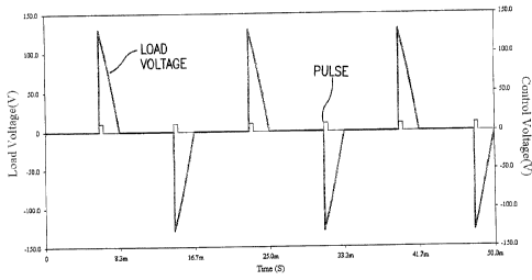
[0030] Figure 12 is a graph of V~,r"" versus V;,-",~ for a conventional RC
phase-
control power controller designed to produce 42 Vr",s output for 120 V,.",s
input.
[0031] Figure 13 is a graph of V~"."" versus V;,-"" for a fixed phase-control
power
controller incorporating the present invention and designed to produce 42
Vr",s output for
120 Vr",s input.
Description of Preferred Embodiments
[0032] With reference to Figure 8, a lamp 10 includes a base 12 with a lamp
terminal 14 that is adapted to be connected to line (mains) voltage, a light-
transmitting
envelope 16 attached to the base 12 and housing a light emitting element 18
(an
incandescent filament in the embodiment of Figure 8), and a voltage conversion
circuit
20 for converting a line voltage at the lamp terminal 14 to a lower operating
voltage. The
voltage conversion circuit 20 may be entirely within the base 12 and connected
between
the lamp terminal 14 and the light emitting element 18. The voltage conversion
circuit 20
may be an integrated circuit in a suitable package as shown schematically in
Figure 1.
[0033] While Figure 8 shows the voltage conversion circuit 20 in a parabolic
aluminized reflector (PAR) halogen lamp, the voltage conversion circuit 20 may
be used
in any incandescent lamp when placed in series between the light emitting
element (e.g.,
filament) and a connection (e.g., lamp terminal) to a line voltage. Further,
the voltage
conversion circuit described and claimed herein finds application other than
in lamps and
is not limited to lamps.
[0034 With reference to Figure 9 that illustrates an embodiment of the present
invention, the voltage conversion circuit 20 includes line terminals 32 for a
line voltage
7
CA 02529519 2005-12-07
and load terminals 34 for a load voltage, a phase-control clipping circuit 36
that clips the
load voltage and that is connected to the line and load tei°minals and
has a three-terminal
thyristor 38 (in this embodiment, a semiconductor controlled rectifier - SCR)
wherein a
conduction angle of the phase-control clipping circuit 36 determines an RMS
load
voltage, and a time-based signal source 40 that sends signals at constant time
intervals to
a gate of the three-terminal thyristor 38 that cause the three-terminal
thyristor to be ON
during time periods that define the conduction angle for the phase-control
clipping circuit
36. In this embodiment that uses an SCR, a full wave bridge 42 is also
provided and the
signals from the time-based signal source 40 have a positive polarity.
[0035] In another embodiment shown in Figure 10, the three-terminal thyristor
38
is a triac. Since the triac is bidirectional (the SCR shown in Figure 9 is
not), the circuit
arrangement may be changed by not including the bridge and by using signals of
either
polarity from the time-based signal source 40. A similar effect is achieved by
using a
pair of SCRs and control signals of opposite polarity.
[0036] The time-based signal source 40 operates independently of line voltage
and thus is independent of variations in the line voltage. The time-based
signal source 40
may be a suitable microcontroller, timer (such as a conventional "555" timer),
or pulse
generator that provides pulses of suitable polarity at constant time
intervals. The timing
of the pulses is set to clip the load voltage at the appropriate place in the
voltage
waveform to provide the desired RMS voltage. Since the freduency of the
voltage
waveform does not change (even though its magnitude might vary), the timing of
the
pulses are set in the circuit for a particular freduency where the lamp is to
be used (e.g.,
50 or 60 Hz). Figure 11 shows the pulses and the resulting clipped load
voltage. Note
CA 02529519 2005-12-07
that the pulses initiate the clipping but are not sustained during the entire
conduction
angle since the three-terminal thyristor remains ON following the pulse. The
pulses need
only have a duration sufficient to initiate conduction in the thyristor.
[0037] In other words, the voltage conversion circuit includes a fixed,
forward
phase-control clipping circuit that forward clips a load voltage and provides
an RMS load
voltage to the lamp, where the phase-control clipping circuit has a time-based
signal
source that triggers conduction of the three-terminal thyristor at constant
time intervals
independently of variations in line voltage magnitude.
[0038] Conventional RC phase-control clipping circuits are very sensitive to
fluctuations in the line voltage magnitude. The present invention provides a
power
controller that operates substantially independently of the line voltage
magnitude by
incorporating time-based pulses to trigger conduction and thereby reduce the
variation of
the conduction angle compared to conventional RC phase-control circuits.
[0039) Figures 12 and 13 illustrate the improvement afforded by the present
invention. Figure 12 shows relationship between Vo,.",~ and V;,~~"s in a prior
art RC phase-
control clipping circuit, while Figure 13 shows the relationship for the
fixed, reverse
phase-control clipping circuit of the present invention. In each instance the
circuit is
designed to produce 42 V,.",~ output for a 120 V~"" input. Note that the
output voltage
varies considerably more in Figure 12 than in Figure 13.
[0040 The description above refers to use of the present invention in a lamp.
The
invention is not limited to lamp applications, and may be used more generally
where
resistive or inductive loads (e.g., motor control) are present to convert an
unregulated AC
9
CA 02529519 2005-12-07
line or mains voltage at a particular frequency or in a particular frequency
range to a
regulated RMS load voltage of specified value.
(0041] While embodiments of the present invention have been described in the
foregoing specification and drawings, it is to be understood that the present
invention is
defined by the following claims when read in light of the specification and
drawings.