Note: Descriptions are shown in the official language in which they were submitted.
CA 02529688 2005-12-16
WO 2004/114265 PCT/US2004/019597
1
SINGhE-hAYER TOUCHPAD AND METHODS OF USE
BACKGROUND OF THE INVENTION
Field Of the Invention: This invention relates
generally to touchpads. More specifically, the
invention relates to a touchpad that can be disposed
on a viewing screen such as a liquid crystal display
(LCD), plasma display (PD), or a cathode-ray tube
(CRT), wherein the viewing screen is used to view data
stored on a stationary object such as a large
television or a computer, or view data on a portable
electronic appliance such as a small television, a
portable computer, personal digital assistant (PDA),
mobile telephone, digital camera, camcorder, a display
for consumer appliances such as a microwave, over,
stove, refrigerator, dishwasher, washing machine,
dryer, and a stereo, wherein the touchpad is capable
of_ determining which zone a user is touching.
Description of Related Art: The state of the art
of touchpads is characterized by a touch-sensitive
device operating on the principles of resistance,
capacitance, optical or other means of sensing touch.
It was determined that the sensing electrodes of a
touchpad can be disposed on a clear substrate, where
the electrodes are made from electrically conductive
materials such as indium tin oxide (ITO).
The substrate can be rigid or flexible, but as a
practical matter, the substrate should be relatively
thin. Good materials for substrates that are
relatively clear and through which a user can see a
viewing or display screen include KAPTON~, MYLART"',
KADADEX°, polyethylene napthalate and other materials
having similar mechanical and electrical properties.
CA 02529688 2005-12-16
WO 2004/114265 PCT/US2004/019597
2
Complete touchpad functionality is generally
characterized as providing cursor control for a
computer, television, or a portable electronic or
consumer appliance. Accordingly, such a touchpad
requires at least two layers of sensing electrodes
when the touchpad uses capacitance sensing technology,
such as that provided by CIRQUE CORPORATION. Multiple
substrate layers and thus multiple or overlapping
layers of electrodes generally results in a touchpad
that is mostly transparent, but can be difficult to
see through when disposed on top of a display.
Attempts have been made to make the substrate
layers and the materials for the electrodes to be
thinner and therefore to have greater transparency.
The attempts so far have still resulted in a display
screen that is uncomfortably dimmed by the touchpad.
Accordingly, what is needed is a touchpad that
does not interfere with viewing a display screen,
wherein at least a portion of the display screen can
be touched to provide touchpad functionality.
When considering typical features of touchpads,
it is necessary to include cursor control and
scrolling capabilities. However, these features are
not always required in the particular device with
which the touchpad is being used.
For example, touch zone control is a feature
wherein the touchpad sends data to the device
indicating in what area the user has made contact.
Thus, touch zones can function as buttons or keys.
However, state of the art capacitance sensitive
touchpads are only able to provide this type
functionality when disposed on top of a display screen
by using multiple layers of substrates and/or
electrodes. The result is that the clarity of the
CA 02529688 2005-12-16
WO 2004/114265 PCT/US2004/019597
3
display screen is generally compromised because of the
touchpad. Accordingly, it would be another advantage
to provide a touchpad that provides touch zone control
to a user, wherein the touchpad provides better
clarity when disposed on top of a display screen.
BRIEF SUMMARY OF THE INVENTION
It is an object of the present invention to
provide a touchpad that includes one signal electrode
and a sense electrode on a single substrate, thereby
improving display screen clarity by not using a second
signal electrode.
15It is another object to provide the one electrode
in a plurality of different locations within the
sensor area of the touchpad.
It is another object to provide the one electrode
and the sense electrode on generally transparent
a
20substrate.
It is another object to provide the single-layer
touchpad wherein the touchpad is capable of detecting
an object touching a zone the touchpad.
of
It is another object to provide the single-layer
25touchpad wherein the touchpad is capable of
simultaneously detecting presence of multiple
the
objects touching a pluralityof zones of the touchpad.
It is another object to provide the single-layer
touchpad wherein the electrodes of the touchpad are
30arranged in a desirable pattern, and wherein the
desired pattern is at least partially visible.
In a preferred embodiment, the present invention
is a single-layer touchpad comprised of a relatively
clear substrate, a first electrode disposed thereon,
CA 02529688 2005-12-16
WO 2004/114265 PCT/US2004/019597
4
and a sense electrode disposed thereon, wherein the
first electrode and the sense electrode are comprised
of a conductive material, wherein the first electrode
in combination with the sense electrode are used to
detect the presence of a pointing object in a zone, or
the simultaneous presence of multiple pointing objects
in multiple zones, and wherein the first electrode
and/or the sense electrode are at least partially
visible so that a pattern is visually detectable on
the display screen.
These and other objects, features, advantages and
alternative aspects of the present invention will
become apparent to those skilled in the art from a
consideration of the following detailed description
taken in combination with the accompanying drawings.
BRIEF DESCRIPTION OF THE SEVERAL VIEWS OF THE DRAWINGS
Figure 1 is a cross-sectional profile view of a
first embodiment of the present invention.
Figure 2 is a cross-sectional profile view of a
second embodiment of the present invention.
Figure 3 is a cross-sectional profile view of a
third embodiment of the present invention.
Figure 4 is a cross-sectional profile view of a
fourth embodiment of the present invention.
Figure 5 is a cross-sectional profile view of a
fifth embodiment of the present invention.
Figure 6 is a cross-sectional profile view of a
sixth embodiment of the present invention.
Figure 7 is a cross-sectional profile view of a
seventh embodiment of the present invention.
DETAILED DESCRIPTION OF THE INVENTION
CA 02529688 2005-12-16
WO 2004/114265 PCT/US2004/019597
Reference will now be made to the drawings in
which the various elements of the present invention
will be given numerical designations and in which the
invention will be discussed so as to enable one
5 skilled in the art to make and use the invention. It
is to be understood that the following description is
only exemplary of the principles of the present
invention, and should not be viewed as narrowing the
claims which follow.
The presently preferred embodiment of the
invention is a single-layer substrate. On this
single-layer substrate, only a single electrode (X or
Y) and a single sense electrode are needed to detect
touching in a zone. The single electrode and the
sense electrode are coupled to a touchpad sensing
circuit, such as the circuit sold by CIRQUE
CORPORATION in its touchpads. The touchpad sensing
circuit determines in which zone of a plurality of
zones is being touched. The touch zones are defined
by the single electrode and the sense electrode as
explained in previously filed patent application
serial number 60/400,843, and is incorporated herein
by reference.
An important aspect of the invention is the
ability to make at least partially visible a desirable
pattern as seen when looking at the display screen.
Assuming that a single-layer touchpad has been
disposed between the display screen and the user, or
the touchpad is visible from the underside of the
display screen, it may be desirable that the touchpad
not be made completely transparent to the user.
For example, the electrodes of the touchpad can
be made visible to the user by taking advantage of
certain characteristics of the materials used in them.
CA 02529688 2005-12-16
WO 2004/114265 PCT/US2004/019597
6
Consider a conductive material for the electrodes
whose width, thickness, color content, and/or
transparency can be varied in order to obtain various
degrees of visibility. Thus, additional materials may
be added to the conductive material used for the
electrodes, wherein the additional materials darken or
lighten the appearance of the conductive material, or
even give the conductive material a color.
The purpose of increasing the opacity of the
electrodes would seem to be contrary to the goal of
making the presence of the touchpad electrodes
unnoticeable. However, making the electrodes at least
partially visible in at least one zone enables a
seller of a device to make a desired image visible to
users or buyers of a product. In other words, the
seller can brand the device with an image, logo, or
word so that there is no mistake as to the identity of
the source of the product when a logo or other service
or trademark is visually discernible to the user or
buye r .
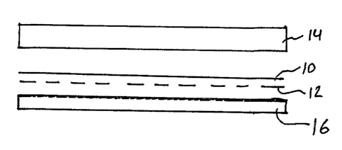
Figure 1 is a cross-sectional profile view of a
first embodiment of the present invention. The
diagram illustrates the layering of materials in a
device utilizing the touchpad of the present
invention. The top layer is the substrate material 10
on which the electrodes 12 of the single-layer
touchpad are disposed. Thus, the substrate material
10 is functioning as a material on which to dispose
the electrodes 12, and as a protective barrier over
the electrodes 12 to prevent damage to them. The next
layer is glass or other cover material 14 used as a
barrier that is disposed over the display screen (not
shown) of the device.
CA 02529688 2005-12-16
WO 2004/114265 PCT/US2004/019597
7
Figure 2 is a cross-sectional profile view of
another embodiment of the presentinvention. In this
diagram, the cover material 14 shown as the top
is
layer of the display screen in device. The
the
electrodes 12 are disposed on substrate material
the
and against the cover material14.
Figure 3 is a cross-sectional profile view of
another embodiment of the presentinvention. In this
diagram, the cover material 14 the top layer. The
is
10substrate material 12 is the nextlayer, and the
electrodes 12 are disposed thereon. The bottom layer
is a liquid crystal display (LCD)of the display
screen of the device.
Figure 4 is a cross-sectional profile view of
15another embodiment of the presentinvention. Figure
4
differs from figure 3 only in the orientation of
that
the substrate material 10 and electrodes 12 are
the
reversed in order.
Figure 5 is a cross-sectional profile view of
20another embodiment of the presentinvention. In this
drawing, the cover material 14 the top layer. The
is
electrodes 12 are shown disposed irectly to the
d
underside of the cover material . Thus, the cover
14
material 14 functions as protection for the display
25screen, and as the protection a substrate for the
and
electrodes of the touchpad.
Figure 6 is a cross-sectional profile view of
another embodiment of the presentinvention. In this
drawing, the cover material 14 the top layer. The
is
30electrodes 12 are underneath, disposed,on top of
and
the LCD screen 16. Thus, the LCD functions as part
of
the display screen, and as the strate for the
sub
electrodes 12.
CA 02529688 2005-12-16
WO 2004/114265 PCT/US2004/019597
8
Figure 7 is a cross-sectional profile view of
another embodiment of the present invention. In this
drawing, the cover material 14 is shown as the top
layer. The next layer is the LCD 16. The electrodes
12 and the substrate material 10 are next. The
electrodes 12 and the substrate material 10 can be
reversed in order.
It should be apparent that the present invention
contemplates many different configurations for
combining the single-layer touchpad of the present
invention with a display screen of the present
invention. These other variations should be
considered to be within the scope of the present
invention.
It is to be understood that the above-described
arrangements are only illustrative of the application
of the principles of the present invention. Numerous
modifications and alternative arrangements may be
devised by those skilled in the art without departing
from the spirit and scope of the present invention.
The appended claims are intended to cover such
modifications and arrangements.