Note: Descriptions are shown in the official language in which they were submitted.
CA 02529758 2005-12-16
WO 2005/011465 PCT/US2004/022176
ELECTROSURGICAL GENERATOR
CROSS-REFERENCE TO RELATED APPLICATIONS
This application is a continuation-in-part of U. S. Application Serial No.
09/904,412 filed 07/12/2001.
STATEMENT REGARDING FEDERALLY SPONSORED RESEARCH
Not applicable.
BACKGROUND OF THE INVENTION
The use of electrotherapy by medical investigators historically reaches back
to
the eighteenth century. In that era, electrotherapy static generators were the
subject
of substantial interest. As the twentieth century was approached,
experimentation
applying high frequency currents to living tissue took place, d'Arsonal being
considered the first to use high frequency currents therapeutically. The use
of high
frequency currents for the purpose of carrying out electrosurgical cutting and
the like
was actively promoted in the 1920s' by Gushing and Bovie. In the 1970s, solid
state
electrosurgical generators were introduced, and a variety of such generators
now are
available in essentially all operating theatres.
When high frequency currents are used for cutting and coagulating, the tissue
at the surgical site is subjected to controlled damage. Cutting is achieved by
disrupting
or ablating the tissue in immediate apposition to the excited cutting
electrode, i.e.,
slightly spaced before it so as to achieve the formation of a cutting arc.
Continuous
sine waveforms generally are employed to carry out the cutting function where
tissue
cells adjacent to the electrode are vaporized. An advantage of this
electrosurgical
cutting procedure over the use of the cold scalpel resides both in an ease of
cutting
and a confinement of tissue damage to very small and shallow regions. In the
latter
regard, cells adjacent the cutting electrode arc are vaporized and cells only
a few
layers deeper are essentially undamaged. These cutting systems, in general,
are
employed in a monopolar manner wherein the cutting electrode is considered the
active one and surgical current is returned from a large, dual component
dispersive
electrode coupled with the skin of the patient at a remote location.
Coagulation also may be carried out using a high frequency generator source
and is accomplished by denaturation of tissue proteins due to thermal damage.
Interrupted or discontinuous waveforms typically are employed to carry out
coagulation. Coagulation is considered generically as including:
(1 ) fulguration in which tissue is carbonized by arc strikes,
(2) desiccation in which the cells are dehydrated, and
CA 02529758 2005-12-16
WO 2005/011465 PCT/US2004/022176
(3) white coagulation in which tissue is more slowly heated to a
coagulum. The interrupted wave based coagulation procedure has been carried
out
with both monopolar and bipolar systems.
In order to obtain cutting with hemostasis to arrest bleeding, present day
electrosurgical generators may be controlled to blend cutting and coagulating
waveforms. To achieve this blend, for instance, a lower amplitude continuous
sine
waveform is combined with higher amplitude coagulate pulses prior to output
voltage
elevation by power amplification procedures or the like.
The electrosurgical cutting reaction has been the subject of considerable
study.
In this regard, some investigators observed that cutting is achieved as the
electrical
conduction of current heats the tissue up to boiling temperatures and the
cells are
basically exploded as a result of the phase change. Another, parallel
mechanism has
been described wherein, as an intense electromagnetic field impinges on
absorbing
tissue, an acoustic wave is generated by the thermal elastic properties of the
tissue.
The origin of the pressure wave lies in the inability of the tissue to
maintain
thermodynamic equilibrium when rapidly heated. See generally:
" Electrosurgery" by J. A. Pierce, John Wiley & Sons
New York, NY
Paramount to the cutting procedure is the generation of an arc within the
evoked vapor phase. When cutting is being performed, the cutting electrode is
not in
mechanical contact with tissue, but rather rides on a vapor film as it is
moved through
the tissue. Thus, it is the separation between the cutting electrode and
tissue which
allows the possibility for arc formation while cutting. With the existence of
this arc,
current flow is highly confined, arcs by their nature being quite localised in
both space
and time, consisting of very short high current density discharges.
Electrosurgical generators generally are configured to derive a requisite arc
formation with an active electrode of fixed geometry. For instance, the active
electrodes may take the shape of a rod or spade-shaped scalpel. Arc formation
requires technique on the part of the surgeon, the electrode being gradually
moved
toward target tissue until the spacing-based impedance is suited for striking
an arc.
The energy creating the arc typically is generated by a resonant inverter
operating at
an RF frequency. Control over such inverters is problematic, inasmuch as the
arc
represents a negative dynamic impedance. In general, some regulation of
voltage
feeding the RF invertors is carried out, however, overall output control is
based upon a
power level selection. Inverter control by output voltage feedback generally
has been
avoided due principally to the above-noted load characteristics of the
necessary arc.
Such attempted control usually evolves an oscillatory instability.
Accordingly, power-
based control is employed with marginal but medically acceptable output
performance.
2
CA 02529758 2005-12-16
WO 2005/011465 PCT/US2004/022176
Currently developing electrosurgically implemented medical instrumentation,
however, has called for active cutting electrodes of highly elaborate
configuration with
a geometry which alters in active surface area during a procedure. Generators
exhibiting a relatively constant power output cannot sustain an arc under such
operational conditions. In this regard, the power output must be variable to
track the
changing shape and size of the active electrode. This, in effect, calls for an
electrosurgical generator capable of producing an RF cutting output under
constant
voltage control and variable power conditions.
Another developing operational requirement for the electrosurgical generator
is
a concern for initial arc formation. Applications of the newly contemplated
systems
call for arc start-up when the active electrode is embedded within and in
contact with
the tissue to be cut. No preliminary impedance defining spacing otherwise
attained by
the technique of the surgeon is available to achieve initial arc formation.
BRIEF SUMMARY OF THE INVENTION
The present invention is addressed to an electrosurgical generator capable of
forming and sustaining a cutting arc at an active electrode exhibiting dynamic
active
surface area characteristics. Studies have revealed that human, as opposed to
porcine, tissue exhibits a quite expanded range of resistances or impedances.
Thus,
earlier contemplated constant voltage control designs tended to overpower the
system when encountering low load resistance. This resulted in excessive
artifacts
in the recovered tissue specimens. On the other hand, the very high resistance
encountered with very dense tissue resulted in excessively diminished power.
Thus,
the instant feedback regulated constant power approach evolved. In effect the
present system performs to provide a substantially uniform electrothermal
cutting
action over a broadened tissue resistance range of from about 100 to about
2000
ohms.
The electrosurgical generator incorporates an input treatment network which
includes a power factor control stage functioning to align incoming current
and
voltage with the attendant traditional advantages. However, this input stage
both
permits use of the generator on a universal, worldwide basis notwithstanding
variations in utility power specifications, and, importantly, establishes an
interim
regulated voltage level which is advantageously utilized by a d.c. link
inverter deriving
a controlled d.c. link voltage.
Other objects of the invention wiH in part, be obvious and will, in part,
appear
hereinafter. The invention, accordingly, comprises the apparatus and method
possessing the construction, combination of elements, arrangement of parts and
steps which are exemplified in the following detailed description.
3
CA 02529758 2005-12-16
WO 2005/011465 PCT/US2004/022176
For a fuller understanding of the nature and objects of the invention,
reference should be had to the following detailed description taken in
connection with
the accompanying drawings.
S BRIEF DESCRIPTION OF THE DRAWINGS
Fig. 1 is a perspective view of the system incorporating the electrosurgical
generator of the invention;
Fig. 2 is a perspective view of the instrument shown in Fig. 1 with a
disposable component being shown removed from a reusable housing;
Fig. 3 is a partial sectional view of the instrument of Fig. 2;
Fig. 4 is a top view of a leaf assembly employed with the instrument shown in
Fig. 2;
Fig. 5 is a general sectional view of a capture component and associated
drive tube;
1S Fig. 6 is a partial sectional view of the forward region of the instrument
of Fig.
2;
Fig. 7 is a front view of the forward portion of the instrument shown in Fig.
1
with components oriented prior to deployment of capture component leafs;
Fig. 3 view is a front view of the forward portion of the instrument of Fig. 1
showing the orientation of components as the leafs of its capture component
are
being deployed;
Fig. 9 is a partial sectional view of the disposable component of the
instrument
shown in Fig. 1 schematically showing a deployment of capture component leafs
to a
maximum diametric extent;
2S Fig. 10 is a partial sectional view of the instrument of Fig. 9
schematically
showing the orientation of the capture component leafs at the completion of
capture
of a tissue volume;
Fig. 11A is a schematic representation of a patient and an electrosurgical
system provided to demonstrate tissue impedance and total impedance;
Fig. 11 B is a schematic representation of a portion of the illustration of
Fig.
11 A;
Fig. 12 is a schematic chart demonstrating the formation of an arc with a
conventional electrosurgically active electrode of fixed geometry;
Fig. 13 is a graph relating time with applied voltage and total resistance for
an
electrosurgical system incorporating the electrosurgical generator of the
invention;
Fig. 14 is a graph showing current levels occurring during the operation of
the
instrument of Fig. 1;
Fig. 15 is a block schematic diagram of the electrosurgical generator and
control features of the invention;
4
CA 02529758 2005-12-16
WO 2005/011465 PCT/US2004/022176
Fig. 16 is an insulation diagram for the electrosurgical generator shown in
Fig.
15;
Figs. 17A and 17B combine as labeled thereon to provide a schematic circuit
diagram showing the EMI filter, front panel switch, and PFC boost converter
S components shown in block form in Fig. 15;
Fig. 13 is an electrical schematic diagram showing a relay solenoid component
employed with contact shown in Fig. 17A;
Fig. 19 is an electrical schematic diagram of a temperature responsive
component employed with the console shown in Fig. 1;
Fig. 20 is an electrical schematic diagram of a power supply dedicated to
provide input power to a motor contained in the reusable housing of the
instrument as
shown in Fig. 2;
Fig. 21 is an electrical schematic diagram of one low voltage power supply
shown in block diagrammatic form in Fig. 15;
Fig. 22 is an electrical schematic diagram of a motor drive shown in block
schematic form in Fig. 15 and further showing the solenoid components of
relays
employed with the invention;
Figs. 23A and 23B combine as labeled thereon to provide an electrical circuit
diagram of a 100KHz inverter, an isolation transformer, a rectifier, an LC
filter, relay
disconnects, an RF inverter, a high voltage transformer and a high voltage
output
stage shown in block diagrammatic fashion in Fig. 15;
Figs. 23C is a schematic pulse diagram illustrating the operation of the
resonant transition phase shift converter shown in Fig. 23A;
Figs. 24A and 24B combine as labeled thereon to provide an electrical
schematic diagram of a link voltage evaluation circuit and a controller for a
power
factor correction boost converter with associated enablement circuitry;
Fig. 25 is an electrical schematic diagram of a primary side power supply;
Fig. 26 is an electrical schematic diagram of a control circuit for providing
phase shift resonant transition control;
Fig. 27A is an electrical schematic diagram of a control circuit for adjusting
d.c.
link voltage;
Fig. 27B is an electrical schematic diagram of a reference voltage deriving
circuit;
Fig. 27C is an electrical schematic diagram of a multiplier circuit for
deriving an
output power monitor signal;
Fig. 27D is a three curve plot illustrating RF output power and voltage
profiles;
Fig. 27E is a representative circuit symbolically depicting the derivation of
a flat
power characteristic;
s
CA 02529758 2005-12-16
WO 2005/011465 PCT/US2004/022176
Fig. 28 is an electrical schematic diagram of a control circuit utilized with
an RF
inverter;
Fig. 29 is an electrical schematic diagram of a circuit for amplifying motor
current;
Fig. 30 is an electrical circuit schematic diagram of a motor current
monitoring
circuit;
circuit;
circuit;
circuit;
Fig. 31 is an electrical schematic diagram of a motor monitoring electrical
Fig. 32 is an electrical schematic diagram of a motor monitoring electrical
Fig. 33 is an electrical schematic diagram of a motor monitoring electrical
Fig. 34 is an electrical schematic diagram showing a derivation of reset and
enable signals;
Fig. 35 is an electrical schematic diagram of a circuit monitoring an output
over- current condition;
Fig. 36 is an electrical schematic diagram of a circuit for monitoring an over-
voltage condition;
level;
Fig. 37 is an electrical schematic diagram of a circuit for monitoring power
Fig. 38 is an electrical schematic diagram of a circuit monitoring for over-
temperature conditions;
Fig. 39 is an electrical schematic diagram of a circuit for monitoring the
level of
d.c. link voltage;
Fig. 40 is an electrical schematic diagram showing a circuit deriving a
footswitch actuation input;
Figs. 41A-41E combine as labeled thereon to describe a programmable logic
device-based circuit with associated output buffering and filtering;
Fig. 42 is an electrical schematic diagram of a power supply;
Fig. 43 is an electrical schematic diagram of a circuit for monitoring a low
voltage power supply;
Fig. 44 is an electrical circuit diagram illustrating the treatment of PLD
signal
inputs and outputs;
Fig. 45 is an electrical circuit diagram of an audio control;
Figs. 46A-46C combine as labeled thereon to describe frequency generation
and test switching components of a PCSM circuit;
Fig. 47 is an electrical schematic diagram of a power supply;
Figs. 48A and 48B combine as labeled thereon to illustrate a circuit for
carrying out a window-based analysis of a return electrode test.
6
CA 02529758 2005-12-16
WO 2005/011465 PCT/US2004/022176
DETAILED DESCRIPTION OF THE INVENTION
In the discourse to follow, the electrosurgical generator of the invention
with
it's attendant boost voltage feature is described in conjunction with a
topology
selected for use with an electrosurgically supported tissue capture
instrument. The
embodiment of that instrument is one which employs only electrosurgical
cutting
current sine waveforms, a cauterization attribute not being incorporated with
the
discussion. However, the instrument, along with variations including those
calling for
cauterization are described in United States patent No. 6,277,083 entitled
"Minimally
Invasive Intact Recovery of Tissue", by Eggers, et al., issued August 21, 2001
and in
United States Patent No. 6,471,659 issued October 29, 2002 entitled "Minimally
Invasive Intact Recovery of Tissue, by Eggers, et al. The electrosurgical
generator of
the invention is described with a configuration based upon a constant voltage
attribute dominating at higher load impedances and a constant power output
dominating at low load impedances. This combination achieves substantially
constant
power output over a somewhat expanded tissue resistance range, i.e., reaching
down to about 100 ohms. and extending upwardly to about 2000 ohms.
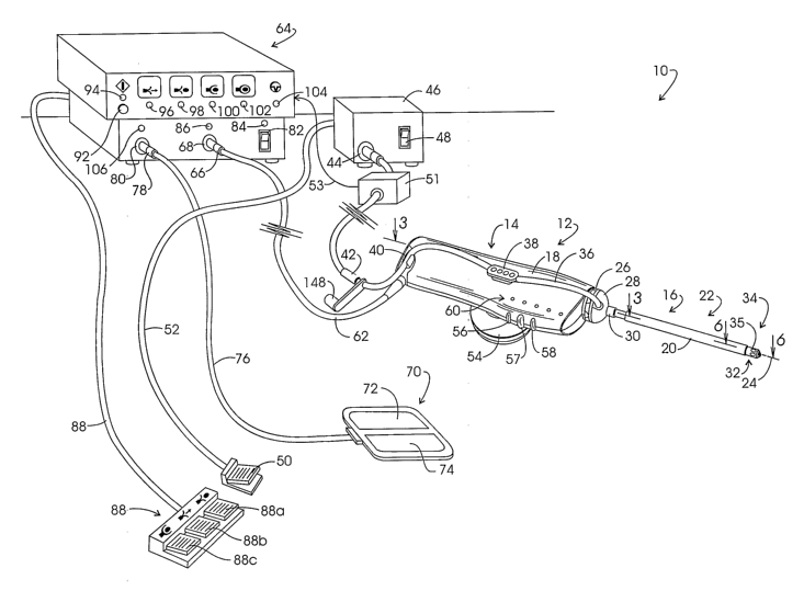
Referring to Fig. 1, the electrosurgical generator of the invention is
depicted as
a component of an electrosurgical intact tissue recovery system shown
generally at
10. System 10 includes a tissue retrieval instrument represented generally at
12
which includes a reusable component represented generally at 14 and a
disposable
component represented generally at 16, the rearward portion of which is
removably
mounted within component 14. The reusable component 14 includes a polymeric
housing 18.
Disposable component 16 includes an elongate delivery cannula represented
generally at 22 having a heat shield 20 and which extends along a longitudinal
cannula or instrument axis 24. The distal end of the delivery cannula 22
extends
through a rotatable threaded connector 26 which is threadably engaged with the
housing 18, as well as through a freely rotatable suction manifold 28 which is
retained in position by a collar 30. The forward region of the cannula 22, as
represented at 32 extends to a distal end or tip represented generally at 34.
A flexible
suction conduit providing a smoke/steam evacuation function is shown at 36
extending from manifold 28 into press fit connection with a connector 38 as
well as
through a connector 40 and intermediate releasable connector 42 to the suction
input
44 of the housing or console of a vacuum system 46. Housing 46 includes an
on/off
switch 48 and is actuated to provide smoke/steamlbody fluid clearing suction
at
conduit 36 by a footswitch 50 coupled to the console 46 via a cable 52.
Smoke/steam
evacuation from distal end 34 is called for to avoid thermal injury to tissue
due to a
migration of steam back along the exterior surface of cannula 22. The vacuum
7
CA 02529758 2005-12-16
WO 2005/011465 PCT/US2004/022176
system extends to tip region 32. In this regard, located at end 32 are four
smoke/steam collection or suction intake ports as are represented at 35.
Cannula 22
is thermally insulated by the insulative sheath 20 to avoid external tissue
damage.
Such thermal insulation is described in copending application for United
States Patent
Serial No. (attorney docket NET 2-098) filed , 2003 and entitled
"Electrosurgical Accessing of Tissue With Controlled Collateral Thermal
Phenomena".
Grip connectors as 38 are positioned on each side of the housing 18 and
function additionally to support a stabilizer handgrip, for example, the
annulus-shaped
grip represented afi 54. Positioned at the forward portion of the housing 18
are three
button switches 56-58 which will be seen to function respectively as an
arm/disarm
switch; an energize position switch; and a start tissue capture switch.
Immediately
above the switches 56-58 on each side of the housing 18 are linear arrays of
LED-
based indicator or cueing lights, one such array being represented generally
at 60.
The visual cues provided by the indicators at 60, from front to rear, provide
a
start/reset cue as a green light; a tissue capture complete cue provided as a
green
light; a start tissue capture cue (above switch 58) provided as a yellow
light; an
energize position cue (above switch 57) provided as a yellow light; and an
arm/disarm tissue capture cue (above switch 56) provided as a green light.
Energization and control is provided to the instrument 12 via a multi-strand
cable 62
which connects with a combined control assembly and electrosurgical generator
console represented generally at 64. Connection is shown through a multi-lead
connector 66 which is coupled to a console connector 68. The electrosurgical
active
electrode assembly of the instrument 12 performs in monopolar fashion. Thus, a
conventional, relatively large, dispersive return electrode assembly as at 70
is
positioned adjacent the skin surface of the patient. Assembly 70 is configured
as
having two electrode components 72 and 74 which are connected via cable 76 and
connector 78 to a console connector 80. Alternatively, a return electrode may
be
positioned on the surface of delivery cannula 22 near its distal end in place
of the
illustrated use of return 70.
Power is supplied to the circuitry at console 64 upon actuation of an on/off
switch 82. When switch 82 is in an "on" orientation, a green visual indicator
LED 84
located above the switch is energized. Proper connection of the cable 62 and
connector 66 with console connector 68 is indicated by an illuminated green
LED 86
positioned above connector 68. This connection test is carried out
by.directing
current to a coding resistor within housing 18. A three-pedal footswitch
represented
generally at 88 is coupled via a cable 90 to the rear panel of console 64. The
three-
pedals, 88a-88c of switch 88 emulate and provide alternative switching with
respective button switches 56-58.
s
CA 02529758 2005-12-16
WO 2005/011465 PCT/US2004/022176
Visual cueing corresponding with that at housing 18 LED arrays as at 60 also
is provided at the console 64. In this regard, a start/reset switch 92 is
operationally
associated with an LED indicator light 94 which illuminates in a green color
upon
actuation of that switch. A yellow position mode visual cue LED representing
an
energization of the noted precursor electrode is shown at 96. This LED
provides a
yellow output during the electrosurgical advancement of the delivery cannula
tip 34
into confronting adjacency with a targeted tissue volume. Next, a green, arm
capture
mode visual cue is provided by an LED 98 to represent an arming of the tissue
capture feature of instrument 12. Once an arm/disarm switch as at 56 or 88a is
depressed the energize position switches as at 57 or 88b are no longer
activatable.
However, the practitioner may return to the position mode by again depressing
an
arm/disarm switch. A yellow capture mode visual cue is provided by an LED 100
to
represent the start of and carrying out of a tissue capture procedure and upon
completion of such capture, a green capture complete mode visual cue is
provided by
a green LED 102. A pause mode condition is represented by the energization of
a
green LED 104. In general, the pause mode is entered during a procedure by
releasing capture switch 58 or footswitch 88c.
Because of the above-noted opportunity for steam migration, it is preferred
that system 10 provide an assurance that the vacuum system as represented at
housing or console 46 be actuated. Preferably, the control assembly of console
64
functions to permit commencement of the procedure only upon a turning on of
system
46. Such a monitoring of system 46 is accomplished with a vacuum actuated
switch
shown at block 51 attached within conduit 36. The monitoring output to console
64 is
represented at arrow 53.
At the time connector 78 of the return electrode 70 is coupled to console
connector 80 and switch 82 is in a power on condition, a patient circuit
safety monitor
circuit (PCSM) carries out a self test. Upon subsequent actuation of
start/reset
switch 94, a fault test with respect to the two electrode components 72 and 74
is
performed. In the event the latter test fails, then both visual and aural
pulsating
warning cues are activated, the visual cue being provided at a red LED 106
located
adjacent connector 80.
Referring to Fig. 2, the disposable component 16 of instrument 12 is revealed
in an orientation prior to insertion within the housing 18 of reusable
component 14. In
the figure, delivery cannula 22 is again seen extending forwardly from a
cylindrically
shaped support housing 108. The forward region of support housing 108 supports
the rotatable connector 26. In this regard, it may be observed that the
connector 26 is
configured with external threads 110 which are fixed for rotation with a
knurled
flange 112. At the rearward end of support housing 108 there is located an
upstanding indexing pin 114 which, during installation of the disposable
component 16
9
CA 02529758 2005-12-16
WO 2005/011465 PCT/US2004/022176
is slidably received within an upwardly disposed elongate slot 116 extending
internally along an elongate receiving cavity 118 within the housing 18.
Internal
threads 120 within the cavity 118 threadably engage the external threads 110
of
connector 26 when the disposable component 16 is inserted within the reusable
component 14.
Positioned opposite indexing pin 114 on support housing 108 are two, spaced
apart electrical contacts 122 and 124 which are oriented to make wiping
contact with
corresponding electrical terminals disposed within housing 18 upon insertion
of
support housing 108 within the receiving cavity 118. Contacts 122 and 124
selectively receive electrosurgical cutting current applied respectively to a
precursor
electrode assembly at tip 32 and the electrosurgical cutting and pursing
cables
associated with a capture component. Those cables extend from the capture
component within delivery cannula 22 to a cable terminator component having
guidance tabs or ears one of which is revealed at 126 slidably mounted within
an
elongate stabilizer slot 130 arranged in parallel with axis 24. A
corresponding
guidance tab and slot combination is found at the opposite side of the support
housing
108. Located forwardly of the slots as at 130 are two additional elongate
drive slots
one of which is shown at 134 similarly arranged in parallel with axis 24. The
outwardly extending ears or guide tabs of a drive assembly drive member extend
from these slots and are seen at 138 and 140. These ears or tabs 138 and 140
support rearwardly disposed driven surfaces which are used to impart forward
movement to the drive assembly. This forward movement functions to deploy a
capture component from delivery cannuia 22. When the support housing 108 is
installed within the receiving cavity 118 of housing 18, these tabs 138 and
140 pass
through oppositely disposed notches shown respectively at 142 and 144 provided
at
the forward portion of housing 18. Similarly, a notch 146 is located forwardly
within
reusable housing 18 to permit passage of the electrical terminals 122 and 124.
As is
apparent, the procedure for installing the disposable component 16 within the
reusable component 14 involves the sliding of disposable support housing 108
within
the receiving cavity 118 and rotating knurled portion 112 of connector 26 to
provide
the engagement of threads 110 with threads 120. The figure also shows a vacuum
forming closure plug 148 which is utilized following the procedure for
blocking
connector 42 of hose or conduit 36 to trap any fluids within the instrument-
connected
forward component of the latter conduit. Finally, a tab 150 is seen extending
through
a forward portion of the drive slot 134. This tab is a component of a drive
assembly
safety stop 304 (Fig. 9) functioning to limit the extent of forward travel
permitted by
the drive member with ears 138 and 140 in accordance with a pre-selected
capture
component diametric extent.
to
CA 02529758 2005-12-16
WO 2005/011465 PCT/US2004/022176
Referring to Fig. 3, a sectional view is presented illustrating the operative
association of the drive features retained within reusable component 14 and
the
driven features of disposable component 16. In the figure, a motor assembly is
represented generally at 160. The assembly 160 is formed of a d.c. electric
motor
160a which is combined with a planetary gear assembly 160b. Assembly 160
provides a rotational output at a stainless steel bellows-shaped somewhat
flexible
coupler 162 and is located within a motor mount chamber 164. Within that
chamber
164, the motor assembly 160 is permitted some self-aligning movement but is
restrained from rotational movement by a torque stop component 166. For the
instant
embodiment coupler 162 extends through a taurus-shaped fluid seal 168 located
within a seal chamber 170. This flexible seal 168 does not constrain the
coupler 162
and permits the noted self-alignment of the motor assembly 160 with respect to
an
elongate rod-shaped translation component 172. Component 172 is seen extending
forwardly to a rotatable and fixed connection with a thrust bearing 174.
fearing 174
provides support against all of the driving forces imposed from the motor
assembly
160. In this regard, the rod-shaped threaded translation component 172 is
threadably
engaged with a transfer assembly represented generally at 176. Transfer
assembly
176 comprises a ball screw or nut component 178 threadably engaged with the
threads of component 172 and a generally Y-shaped yoke 180 which is configured
having spaced apart drive members configured to extend to a position spaced
from
but aligned for driven engagement with the tabs or ears 138 and 140 (Fig. 2)
of a
drive member when the support housing 108 initially is inserted in the
receiving cavity
118. To assure non-binding performance of the above drive components, it is
necessary to avoid axial creep phenomena and the like which may be manifested
as
a compression of bellows 162. In general a sleeve is provided over the output
drive
shaft of assembly 160, while a corresponding stepped-down diameter at
component
172 provides a shoulder against which the coupler 162 abuts.
Electrosurgical cutting current as well as control inputs and outputs are
introduced from cable 62 to the housing 18. Two of the multi-lead components,
certain of which are revealed at 180, extend to a contact clamp 182 which
retains
two contacts for supplying electrosurgical cutting energy to contacts 122 and
124 of
the disposable component 16.
Fig. 3 also reveals some details of the tip 34 of delivery cannula 22. That
tip
34 is depicted as it is utilized for relatively smaller tissue volumes, for
example,
encompassed within a diametric extent of about 10mm. The tip incorporates four
precursor electrode components arranged in a cross shape symmetrically about
longitudinal axis 24. Two of the electrosurgical cutting portions of the
precursor
electrodes are revealed at 184 and 185 located just forwardly of a truncated
cone-
shaped ceramic (alumina) protective tip 190. Tip 190 functions to provide an
arc-
11
CA 02529758 2005-12-16
WO 2005/011465 PCT/US2004/022176
resistant or arc isolating tip portion preventing its breakdown. Rearwardly of
ceramic
tip 190 are polymeric tip components 192 and 194 which are coupled to delivery
cannula 22. The fatter component 194 is seen to carry the earlier described
suction
ports 35. The former component 192 provides a ramp structure for a sequence of
five thin stainless steel leafs of a capture component, the tips of which
carry braided
stainless steel pursing cables which are electrosurgically excited for cutting
purposes and which create a pursing action cuffing to form a cage-like
structure
around a targeted tissue volume. Alternatively, the precursor electrode,
leafs,
pursing cable and cannula may be constructed of non-ferromagnetic materials
(e.g.,
titanium, nitinol) to enable use of this device with magnetic resonance image
guidance
of a biopsy procedure. Drive imparted to these capture component leafs
emanates
from the yoke 180 and drive member ears 138 and 140. Each of these leafs
terminates in eyeiets at its leading edge certain of which are represented
generally at
196. The polymeric tip components 192 and 194 cooperate to form a guidance
assembly represented generally at 198 which functions to direct the leafs,
appropriately spaced apart and at a proper attack angle, in a capture
maneuver. That
attack angle for the instant embodiment is 45°.
Delivery cannula 22 has a relatively small diametric extent, for example,
about
5mm. Within its forward portion 32 there is disposed an earlier-noted capture
component comprised of a pentagonally-shaped stainless steel elongate leaf
structure with a leading edge formed with dual eyelets which carry a five
pursing
cable assembly. Referring to Fig. 4, the capture component is represented
generally
at 200 at a stage in its fabrication prior to the attachment of the noted
pursing cables
along with polymeric guide tubes. As revealed in the general sectional view of
Fig. 5,
the capture component 200 has a generally pentagonal cross sectional
configuration
initially chemically milled from flat stainless steel stock such that the
forward portion
202 is formed with a sequence of five leafs having a thickness of 0.003 inch
and a
widthwise extent of 0.080 inch. The five leafs are shown in these figures at
210-214
and extend from a pentagonal base portion 218 to the noted dual eyelet tips
196.
Each of the leafs 210-214 is chemically milled with a somewhat centrally
disposed
groove extending longitudinally along their lengths. Within this groove, as
seen in Fig.
5, there is adhered a polyamide flexible guide tube. These guide tubes are
quite small,
having, for example, an outside diameter of about 0.020 inch and a wall
thickness of
about 0.0015 inch. The guide tubes are shown in Fig. 5 at 220-224 as being
adhesively attached to respective leafs 210-214. Each of the guide tubes 220-
224
slidably guides a pursing cable as shown respectively at 230-234. These
multistrand
stainless steel cables have a diameter of about 0.006 inch. The polyamide
guide
tubes 220-224 are attached by initially adhesively coupling them to the noted
troughs.
Then, the tubes are bonded to a corresponding leaf within the chemically
milled
12
CA 02529758 2005-12-16
WO 2005/011465 PCT/US2004/022176
groove utilizing an electrically insulating coating material and process which
achieves
bonding and provides requisite electrical insulation for the entire capture
component
assembly 200. The coating, which has a thickness of about 0.001 inch, is a
vapor-
phase-polymerized conformal coating marketed under the trade designation
"Parylene". Parylene is the generic name for members of a polymer series. The
basic
member of the series, called Parylene C is poly-para-xylene, a completely
linear,
highly crystalline material. Such coatings are available from Parylene coating
service
companies such as Specialty Coating Systems, (SCS) of Indianapolis, IN. Fig. 4
reveals the eyelet structure at the leading edge of capture component 200. The
leading edges containing the eyelets are bent outwardly from the orientation
shown
prior to the attachment of cables through them. Further, the capture component
200 is
weldably attached to a drive tube or drive rod 236 which extends rearwardly
into
support housing 108 and into engagement with the drive member associated with
the
tabs or ears 138 and 140 (Fig. 2).
Referring to Fig. 6, the forward region 32 and tip 34 of the delivery cannula
22
are revealed in sectional detail. In the figure, the delivery cannula 22 with
heat shield
is seen extending forwardly to the earlier-described polymeric
(polyetherimide) tip
component 194. Heat shield 20 and portions of cannula 22 are electrically
insulated
with a 5 mil thick polyolefin shrink tube 238 extending to a border 240 at
component
20 194. Note the insulative air space 21 between heat shield 20 and cannula
22.
Inboard from the internal surface of the delivery cannula 22 are the five
capture
component leafs in pentagonal configuration, portions of two of which are
shown at
210 and 212. Extending next inwardly inboard is a stainless steel support tube
242
which is mounted at the rearward portion of the support housing 108 of
disposable
component 16 and extends forwardly through the delivery cannula 22 to a flared
region 244 engaging polymeric tip component 192. This flaring is found to be
helpful in
permitting the support tube to overcome the rather substantial forwardly
directed
forces occurring during forward deployment of the capture component leafs and
cables. Extending inside the support tube 242 is an electrosurgical precursor
electrode tube 246 which also extends to the rearward portion of support
housing
108 for purposes of both support and receiving electrosurgical cutting energy
transmitted through electrical contact 122 (Fig. 2). As the precursor
electrode tube
246 extends rearwardly, it is electrically insulated from support tube 242 by
a
polymeric shrink wrap -248. -
The precursor electrodes are mounted as a subassembly of four stainless
steel electrode wires having a generally elongate L-shape, two of which are
shown
in conjunction with electrodes 184 and 185. In this regard, the elongate
components
of these electrodes 184 and 185 are shown respectively at 250 and 251
extending
into a subassembly tube 252. Four such electrode assemblies are crimped inside
this
13
CA 02529758 2005-12-16
WO 2005/011465 PCT/US2004/022176
tube 252 and that tube 252, in turn, is crimped within the forward portion of
the
precursor electrode tube 246. It has been found that the utilization of four
cutting
surfaces for the electrodes, arranged in a cross-shaped pattern, provides
preferable
instrument positioning results. Such an arrangement of confronting electrode
surfaces is revealed, for example, in connection with figures 7 and 8. In
general, the
severing portions of the precursor electrodes will be extending normally to
the
longitudinal axis of the instrument and will be configured to directly
confront the tissue
being severed during the insertion or placement of the instrument in a
confronting
relationship to the involved tissue volume. The dimensional extent of the
confronting
severing portions of these precursor electrodes is selected to provide an
effective
length less than the corresponding maximum diametric extent developed by the
capture component. In Fig. 6, that extent may be observed at stylized dashed
locus
of movement line 254. In deploying the capture component 200, the forward or
leading edge thereof containing the noted arc forming cables will cut a path
somewhat similar to that shown at dashed line 254 reaching the capture
component
predetermined maximum peripheral diametric extent at a point in the deployment
when
pursing commences as cable forward movement no longer is permitted to effect a
contraction and enclosure of an encapsulated tissue volume including a target
tissue
volume represented symbolically at dashed line 256. Accordingly, power must be
supplied to this cutting electrode cable assembly to sustain an arc while
accommodating initially for its expanding surface area, i.e., length and then
for its
contraction toward its procedure terminating very small surface area extent.
This
may be contrasted with a conventional electrosurgical scalpel having a fixed
configuration throughout a cutting procedure. With the instant procedure, both
the
precursor electrodes 184-187 and the cables 230-234 at their confronting
portions
are initially and at any re-start embedded in tissue as opposed to being
spaced from a
tissue surface, a condition ameliorated by the application of a boost voltage
level to
create an arc at the initiation of electrosurgical cutting, whether at the
outset of the
procedure, or following a stop in the procedure. Preferably, this boost
condition (e.g.
1100 volts, peak-to-peak) is present for only a minimal boost interval
sufficient to
create a cutting arc. While it is possible to extend this boost interval to
the extent of
the entire procedure including both the positioning procedure using precursor
electrodes and for capturing a specimen with pursing cables, the consequence
is the
generation of excessive power during the biopsy procedure which results in
artifacts
at greater depth of thermal injury to the biopsy specimen and surrounding
healthy
tissue.
Fig. 6 also reveals that polymeric tip component 194 functions as a guide for
the leafs 210-214. Similarly, polymeric tip component 192 is configured with
five
ramps arranged at a 45° angle with respect to the instrument axis 24.
One of those
14
CA 02529758 2005-12-16
WO 2005/011465 PCT/US2004/022176
ramps is shown at 258 in conjunction with leaf 210. These ramps provide for
the 45°
angle of attack of leafs 210-214 as they emerge during a capture procedure.
In general, the precursor electrodes 184-187 will have a tissue cutting and
confronting length of about 6.5mm to 7.Omm for employment with a maximum
effective
S capture diameter for the capture component 200 of 10mm. Similarly, where
that
efFective diameter expands to 20mm, the expanse of the precursor electrodes or
their
lengthwise confronting extent will be about 10mm. When configured having one
of
the larger lengthwise extents, the electrodes are slightly canted forwardly
and are
made resilient so as to be capable of flexing forwardly as the
electrosurgically
excited pursing cables physically contact the precursor electrodes. During
this
procedure, the precursor electrodes are open-circuited and permitted to be
reenergized as they are urged into alignment with the capture component leafs.
This
temporary re-energization of the longer precursor electrodes is found to be
beneficial
as the electrodes retract or bend toward larger tissue samples being captured.
Figs. 7 and 8 present front views of the delivery cannula 22 tip 34,
illustrating
in particular the orientation of the precursor electrodes, as well as the
leafs and
cables in a retracted state in Fig. 7 and as the leafs and cables emerge in
Fig. 8. in
the procedure initiation orientation of Fig. 7, the active area extent
exhibited by the
electrosurgically cutting portions of cables 230-234 is somewhat small but
slightly
larger than at full pursing at the completion of the procedure. In Fig. 7, the
five leaf
tips of leafs 210-214 are visible in connection with portions of the pursing
cables 230-
234. When in this orientation, the precursor electrodes 184-187 will have been
excited to form an arc while the instrument 12 is maneuvered into an
orientation
wherein the tip 34 is in confronting relationship with the targeted tissue
volume. The
precursor electrode structure then is deactivated (open circuited) and the
capture
component 200 is deployed in conjunction with the arc forming excitation of
pursing
cables 230-234 with electrosurgical cutting energy. However, inasmuch as the
cables are embedded in tissue, a boost voltage is called for, for a boost
interval
adequate to evoke formation of a cutting arc between the active portions of
cables
230-234 and confronting tissue.
Fig. 8 shows that as the leafs 210-214 are deployed, the pursing cables 230-
234 are being "played out" and the effective diametric extent of the capture
component is expanding to circumscribe the targeted tissue volume to be
removed.
To provide the expansion and subsequent pursing arrangement, note that cable
230
slides through guide tube 220 and is attached to the flip of leaf 214. Cable
231 slides
through guide tube 221 and is attached to the tip of leaf 213. Cable 232
slides through
guide tube 222 and is attached to the tip of leaf 212. Cable 233 slides
through guide
tube 223 and is attached to the tip of leaf 211; and cable 234 slides through
guide
tube 224 and is attached to the tip of leaf 210.
is
CA 02529758 2005-12-16
WO 2005/011465 PCT/US2004/022176
Referring to Fig. 9, a partial sectional view of the support housing 108 of
disposable component 16 is provided. In the figure, the support tube 242 is
seen to
extend to engagement with a bulkhead 270 at the rearward portion of support
housing 108. The tube 270 is retained in position by a collar 272. Extending
through
the support tube 242 is the earlier-described precursor tube 246 absent the
insulative
shrink wrap covering 248. Precursor electrode tube 246 is seen to be in
abutting
contact with electrical contact 122. With this arrangement, electrosurgical
cutting
energy can be conveyed from the contact 122 into the tube 246 and thence to
the
precursor electrodes 184-187. The rearward portion of the capture component
drive
assembly is represented generally at 274 and is seen to include the earlier-
described
drive tube 236 and a drive member 276. Drive member 276 is shown in a
sectional
view wherein the integrally formed ears 138 and 140 (Fig. 2) are not seen.
However,
note that it is coupled to the end of drive tube 236 and both that tube 236
and the drive
member 276 slidably move over support tube 242 along the instrument axis 24.
The
yoke 180 described in connection with Fig. 3 engages the ears 138 and 140 to
move
drive assembly 274 forwardly by virtue of its abuttable engagement with ears
or tabs
138 and 140 (Figs. 2 and 3).
Pursing cables 230-234 extend rearwardly outboard of the drive tube 236 into
the internal cavity 278 of support housing 108. Two of these pursing cables
are
symbolically represented at 230 and 231. These cables slidably extend through
corresponding five channels extending through drive member 276, one of which
is
shown at 280. The cables 230-234 extend further to a fixed connection with a
polymeric cable terminator component 282. Component 282 is slidably mounted
upon
support tube 242 and includes a forward ferrule or collar 284 which is press-
fitted
over the cables 230-234. The cables then extend through a central flange
portion 286
of component 282 for rigid and electrical connection with a rearward ferrule
or collar
288. Collar 288, in turn, is coupled to a flexible electrical cable 290
connected to
electrical connector 124, which follows the cable terminator component 282 as
it
slides forwardly. Accordingly, electrosurgical cutting energy is supplied to
the cables
230-234 from connector 124, cable 290 and the ferrule 288. Cable terminator
component 282 is stabilized by two outwardly extending ears or tabs, one of
which is
described in connection with Fig. 2 as a tab 126 riding within stabilizer slot
130.
Positioned forwardly of cable terminator component 282 is a cable stop 292.
The
collar-shaped stop 292 is adhesively fixed to support tube 242 at a location
defining
the maximum diametric extent developed by the leading edge of the capture
component 200 leafs. That maximum diametric extent is represented in the
instant
figure in symbolic fashion as extending over a tissue volume and about halfway
over
a targeted tissue volume shown in dashed line fashion at 294. It has been
determined
that a more reliable capture is achieved by positioning a compression spring
as at 293
16
CA 02529758 2005-12-16
WO 2005/011465 PCT/US2004/022176
between stop 292 and component 282. This arrangement is described in detail in
copending application for United States Patent Serial No. (attorney docket Net
2-097)
entitled: "Electrosurgical Method and Apparafius With Dense Tissue Recovery
Capability" filed 2003. With the orientation of the capture component 200
shown, the cable terminator component 282 will have commenced to abuttably
engage the cable stop 292 through spring 293 to effect a tensioning of the
pursing
cables 230-234 as the drive assembly 274 continues to be driven forwardly by
motor
assembly 160, translation component 172 and transfer assembly 176 (Fig. 3). A
drive
safety stop mechanism comprised of stop member 304 is fixed within cavity 278
to
limit the forward movement of drive assembly 274 beyond a location
representing a
full pursing or contracting of the capture component 200 for the elected
maximum
diametric extent of capture. Such unwanted movement may occur, for example,
with
a failure of cable stop 292 to halt forward movement of cable terminator
component
282. As drive assembly 274 continues to be driven forwardly and the drive
member
276 approaches adjacency with safety stop member 304 the leafs of capture
mechanism 200 will be pursed mutually inwardly together to define a
confinement
structure surrounding the tissue volume to be removed. As this occurs, the
relative
lengths of active electrode cutting components of the pursing cables commence
to
diminish to ultimately assume a very small active cutting area. This
orientation is
revealed in Fig. 10 which shows the positioning of components subsequent to
the
procedure-based orientations represented in Fig. 9. Drive member 276 and its
associated drive tube or rod 236 of drive assembly 274 are seen to have been
driven
further forwardfy, drive member 276 being in spaced adjacency with respect to
the
drive safety stop mechanism 302. Cable terminator component 282 is in abutting
engagement with cable stop 292. This has caused a tensioning of the five
cables
230-234 and a pursing encapsulation of the target tissue 294 and surrounding
tissue
volume which has been carried out by the capture leafs of the capture
component
200.
The stress load carried by the cables 230-234 now is of an extent wherein
the control features of the control assembly will detect a forward stall
condition on
the part of motor 160a. As this occurs, cutting energy to the cables 230-234
is
terminated and motor assembly 160 is energized to be driven in reverse.
Accordingly,
yoke 180 will release from freely abutting engagement with tabs or ears 138
and 140
of drive member 276 and that member will return to a home position. The
reusable
component 14 of the instrument 12 thus is reoriented for a next utilization.
In general,
the practitioner then decouples coupler 42 of the suction line 36 and traps
the fluid
therein by inserting the plug 148 within it (Fig. 2). The disposable component
16 then
is removed by unscrewing the forward threaded connection at connector 26 and
ears or tabs 138 and 140 may be manually returned to abutment with the latch
17
CA 02529758 2005-12-16
WO 2005/011465 PCT/US2004/022176
assembly 296. This causes the capture component 200 to approximately reassume
the orientation shown in Fig. 9, making the retrieved tissue specimen readily
accessible to the practitioner.
Referring again to Fig. 1, the procedure carried out with system 10 initially
involves the administration of a local anesthetic agent at the skin level in
the region of
an intended biopsy. Switch 82 is actuated to turn on the console 64 and cable
62 is
attached at connector 68. Upon a successful testing of the connection, green
LED 86
illuminates. The practitioner presses the start/reset button 92 on console 64,
whereupon a patient safety circuit monitor test is carried out, the red LED
106 and an
aural cue providing a pulsed output in the event of failure of this test.
Disposable
component 16 is mounted within the reusable component 14 and a skin incision
using
a cold scalpel to a depth of about 4mm and a width of 2mm wider than the
maximum
width of the tissue volume to be removed is made. The smoke/steam evacuator 46
is
turned on from footswitch 50 and the tip 34 of the delivery cannula 22 is
extended
into the incision such that the precursor electrodes at its tip are at least
3mm below
the surFace of the skin. Thus, these electrodes initially are embedded within
the skin.
A positioning mode then is commenced with either the depression and continued
depression of energize/position footswitch 88b or housing 18 button switch 57
to
effect first boost then normal cutting energization of the precursor
electrodes. LED
96 is illuminated as well as the corresponding LED at array 60. An aural cue
is
provided as a steady tone. The tip 34 of the delivery cannula 22 is advanced
to a
position of confronting adjacency with the tissue volume to be removed. When
this
position is reached, the positioning mode is terminated (footswitch 88b is
released or
button switch 57 is released), the arm/disarm tissue capture button or switch
56 or
footswitch 88a is depressed momentarily, the LED above that switch as well as
LED
98 are illuminated, and the system 10 enters an arm capture mode. During this
mode,
switches 57 and 88b are disabled. The start capture button or switch 58 or
footswitch 88c is then depressed and continues to be depressed, the LED above
switch 58 as well as LED 100 are illuminated, a capture mode commences, and
the
motor 160a (Fig. 3) turns on to advance the yoke assembly 180 forwardly for an
interval of one half second during which time motor current is monitored to
assure
proper operation. As the yoke 180 engages the ears 138 and 140 of drive member
276, motor assembly 160 is turned off. The electrosurgical generator applies
first
boost, then normal cutting energy to the pursing cables 230-234 (Fig. 7) and
following
a one half second delay, motor assembly 160 is energized to start deployment
of the
capture component 200. During energization of pursing cables 230-234 the noted
steady tone is provided from console 64. This capture mode continues until the
capture component 200 orientation described in connection with Fig. 10 is
reached.
At that juncture, a forward stall condition is witnessed at motor 160a,
forward
is
CA 02529758 2005-12-16
WO 2005/011465 PCT/US2004/022176
energization of the motor assembly 160 is terminated and the motor is reversed
to
withdraw the transfer assembly 176 to its initial home position. LED 102 on
console
64 as well as the corresponding LED output at array 60 are illuminated and the
tone
representing application of electrosurgical current is terminated. Delivery
cannula 22
is removed from the patient, plug 148 is attached to vacuum connector 42 and
connector 26 is rotated to permit removal of the disposable unit 16. Upon
removal of
the disposable unit, ears or tabs 138 and 140 may be manually retracted to
engagement with the latch assembly 296 to permit capture component 200 to
assume
an orientation represented at Fig. 9 for tissue specimen access.
Electrosurgical energy is applied at the noted boost voltage level at the
initiation of the procedure with respect to both the positioning mode and the
capture
mode or recommencement following any pause activity that occurs in conjunction
with the release of fingerswitch 58 or footswitch 88c and the illumination of
LED 104.
The extent of this application is for a boost interval extending at least
until the
commencement of formation of an arc to permit cutting or for some
predetermined
boost interval based upon experience, for example, three eighths second.
-Control over the cutting energy supplied from the electrosurgical generator
to
the pursing cables 230-234 is predicated, inter alia, upon a conventional
design
approach wherein the power developed must be effective to sustain an arc so as
to
cut while not causing excessive damage to tissue adjacent the cut, the
instrument, or
the recovered tissue specimen. With system 10, however, additional criteria
arise.
That active electrode manifested as the tissue encountering portions of cables
230-
234 is changing in surface area extent during the procedure. It initially
commences to
be excited under boost voltage having a geometry somewhat resembling a point
source. Then it increases in peripheral extent resembling a gradually
expanding line
source, whereupon it then returns to assume a geometry approaching a point
source.
Thus, the system 10 generally is involved with a cable-based variable
performance
requirement. Additionally, at the commencement of the procedure, the active
electrode assembly, whether precursor electrodes or capture component cables,
is
embedded in tissue and boost voltage is called for during the noted boost
interval to
create a vapor and cause the commencement of an arc extending, for instance,
between the cutting portions of cables 230-234 and the tissue being cut. In
effect, it
is this arc and not the cables per se that creates the cut. The active
electrode
portions merely slide within a vapor developed from adjacent tissue cell
layers.
Accordingly, the control must sustain the arc throughout the procedure.
Conventional electrosurgical generators are designed to perform in
conjunction with an active electrode of fixed configuration or geometry such
as a
blade or rod. Development of a necessary cutting arc is achieved by the
technique or
experience of the surgeon who causes initial arc formation or creation by
moving the
19
CA 02529758 2005-12-16
WO 2005/011465 PCT/US2004/022176
active electrode toward the targeted tissue until the arc forms, for example,
at about
one mm spacing. Looking to Figs. 11A and 11 B, this technique is portrayed. A
patient
is depicted at 310 whose back is abuttingly engaged with a large dispersive
electrode
312 which provides a return to an electrosurgical generator 314 as represented
at
S line 316. Generator 314 feeds tissue cutting energy to an active electrode
or
eiectrosurgical scalpel 318 of fixed geometry as represented at line 320.
To achieve arc commencement, the efectrosurgical generator output must
confront an impedance of adequate range, for example, 1300 to 1500 ohms. This
impedance is resistant in nature and comprises the resistance, Rt;ssUe,
exhibited by the
body of the patient 310, as represented by the distance from B to C, the value
ranging
from about 300 ohms to about 500 ohms, in combination with the impedance or
resistance developed by the active electrode spacing from tissue 322 of
patient 310.
Fig. 11 B illustrates, in enlarged fashion, that spacing, L9, as the distance
from A to B.
Looking to Fig. 12, this resistance, RAB is plotted at dashed lines 324 and
326 with
respect to variations in the distance, Lg. Note that at values of L9 greater
than about
2mm as shown at dashed fine 324, the resistance RAB approaches infinity and no
arc
is developed as labeled. However, as the active electrode of fixed
configuration
approaches a distance, Ls of about 1 mm, a resistance of about 500 ohms to
about
1000 ohms is witnessed which, when combined with the resistance, Rtiss~e (B to
C)
permits an arc to be formed as labeled. With the proper resistance, Rtota~,
represented
from A to C, the cutting arc will be sustained in accordance with the
generalized
expression: Rfofal = ~~ss~e and R~~~. With the above arrangement, conventional
electrosurgical generators are operated in conjunction with a fixed output
power and
a variable applied voltage. The output power levels thus are maintained within
a safe
range, for example, from about 80 watts to about 100 watts. Studies carried
out with
the instant system reveal that uniform electrothermal power is call for over a
substantial tissue resistance range. Human fatty tissue exhibits high
resistance while
very dense tissue exhibits very low resistance. As a consequence, the system
10
should be capable of uniform performance over a load resistance range of from
about
100 ohms to about 2000 ohms. That calls for a substantially constant power
output
characteristic.
The equivalent of the arc formation otherwise created by manual electrode
spacing carried out with the technique of the surgeon is achieved with system
10
even though the active electrode initially and at the time of any restart is
embedded in
tissue with no initial spacing available. Application of the short term
(tboost) boost
voltage (Vboost) causes a vaporization of the tissue cell structure adjacent
the initially
exposed and tissue embedded active portions of cables 230-234 or the precursor
electrodes. This evokes the equivalent of an initial spacing to achieve
requisite
impedances for arc commencement. The interval of application of the boost
voltage
CA 02529758 2005-12-16
WO 2005/011465 PCT/US2004/022176
may be, as noted above, of minimal fixed duration, for example, about 500
milliseconds or less or may be defined by the creation of the arc following
the
application of this boost voltage. The impedance change, Rtotai, at the
formation of the
arc represents a quite abrupt alteration and results in a corresponding abrupt
drop in
output current flow. Accordingly, the formation of the arc may be detected
readily to
carry out boost voltage application termination.
Referring to Fig. 13, the performance of system 10 in connection with an
experiment carried out using slab bacon and a capture maximum diametric extent
of
millimeters is portrayed. The experiment utilized a generator exhibiting a
constant
10 voltage characteristic as described in copending United States application
Serial No.
09/904,412 (supra). In the figure, total resistance in terms of ohms, as
computed, is
plotted with respect to time. Additionally, applied, peak-to-peak voltage is
plotted with
respect to that time, and the current witnessed at d.c. motor 160a is plotted.
At the
commencement of the procedure, prior to the application of boost voltage, the
total
resistance was equal to the tissue resistance, R~;SSUe as earlier described in
connection with distance B-G in Fig. 11A. That 500 ohm level is represented at
dashed line segment 328. Boost voltage was applied to the cable electrodes 230-
234
to commence the boost interval at a boost voltage of 1400 volts peak-to-peak,
as
represented at line 330. This boost voltage was imposed for an interval,
Tboost, as
represented at line segment 332, of 500 milliseconds, whereupon the applied
boost
voltage abruptly dropped as represented at solid line segment 334. During the
boost
interval, following about 200 milliseconds, as represented at dashed line
segment 336
and somewhat vertical dashed line segment 338, an arc was formed and total
resistance abruptly elevated to about 1500 ohms at a point in time near the
termination
of the fixed boost interval. This arc formation occasioned the adding of about
1000
ohms of arc resistance to the tissue resistance as the value for f?~otai. As
represented at line segment 334 the applied voltage was dropped to a normal
cutting
voltage level represented at horizontal solid line segment 342. This applied
normal
cutting voltage is seen to have been at a level of 1000 volts peak-to-peak.
Essentially
simultaneously, as represented at vertical dashed line segment 344, motor 160a
was
energized following a head start interval, ths, from the application of boost
voltage.
With the energization of motor assembly 160, the leafs 210-214 commenced to be
extended as the cables 230-234 began to be played out toward a peripheral
extent of
maximum diameter. As this occurred, the length and consequent surface area of
the
cables engaged in active cutting of tissue expanded and the corresponding
total
resistance commenced to drop as represented by the dashed curve segment 346.
As the maximum peripheral extent of the leaf tip portions and active cable
cutting
lengths reached the maximum value, as represented at vertical dashed line 348,
total
21
CA 02529758 2005-12-16
WO 2005/011465 PCT/US2004/022176
resistance for the cut voltage level reached a lowest value. At this juncture,
applied
current also reached a maximum value with a concomitant power increase.
As the time interval of the procedure continued beyond the time represented at
vertical dashed line 348, the active surface area of cables 230-234 employed
in
cutting tissue reduced as forward contraction or pursing ensued and the
effective
cable length engaged in tissue cutting reduced. This reduction in active
surface area
evoked a total resistance increase as represented by the curved dashed line
segment
350. During this interval, the d.c. motor current which commenced at line
segment
344 gradually increased as represented at dashed line segment 352 until motor
stall
threshold was reached as represented at the current level 353, whereupon motor
current was terminated as represented at dashed line segment 354.
Simultaneously,
normal cutting voltage was terminated abruptly as represented at dashed line
segment 356. Following the procedure, the total resistance, Rtota~, returned
to the
value of the tissue resistance, Rt;ssue~ as represented at line segments 358
and 360.
Referring additionally to Fig. 14, a plot of current output and control timing
occurring during the interval represented by the procedure carried out in
connection
with Fig. 13-is revealed. In the figure, the time of applying voltage,
commencing at the
noted boost level is represented by vertical dashed line segment 362. The
voltage
was applied at a boost level and continued as represented at horizontal dashed
control line segment 364 and this boost voltage level terminated at the
completion of a
500 millisecond boost interval as represented at vertical dashed line segment
366.
Applied voltage then was retained at a constant voltage level represented at
horizontal control line segment 368. During the application of boost voltage
as
represented at control line segments 362 and 364, current levels, encountering
initial
lower tissue impedance, abruptly rose as represented at curve segment 370 and
was sustained at the peak level thereof as represented at 372 for an interval
of about
200 milliseconds. At the termination of that interval, an arc developed to
impose arc
resistance occasioning an abrupt current drop represented at curved portion
372. It
is during that 200 millisecond interval that the effective initial spacing is
carried out by
vaporization of tissue cells and the cuffing arc is developed. The plot
represented by
these current levels also may be considered to correspond with power
dissipation
during the procedure. The current drop represented at curved segment 372 may
be
detected for purposes of terminating the boost voltage and thus established
the boost
interval in correspondence with arc formation.
Returning momentarily to Fig. 13, and recalling that with system 10, power
applied from the electrosurgical generator is varied in accordance with the
application
of boost voltage and with the changing of the cable electrode geometry, for
the
example at hand, power dissipation may be evaluated. The commencement of the
application of boost voltage is represented at line 330, a tissue resistance
of 500
22
CA 02529758 2005-12-16
WO 2005/011465 PCT/US2004/022176
ohms having been encountered. Accordingly, until the arc was formed, under an
applied boost voltage of 1400 volts peak-to-peak, a power dissipation of about
500
watts occurred. However, that power was produced in a highly constricted
region
for the very short interval occurring until the arc was formed as represented
at
dashed line 338, for an example, the interval of about 200 milliseconds
discussed
above. As soon as the arc was formed, as represented at dashed line 338, the
impedance represented by the arc was added to the 500 ohm tissue impedance and
the power dissipation dropped to about 167watts which, although slightly high,
remained only until the removal of boost voltage as represented at vertical
line
segment 334. Normal cutting voltage at 1000 volts peak-to-peak then ensued
with a
power dissipation of about 85 watts. However, now the expansion of the active
electrodes commenced, power again rose as the total resistance dropped to
about
800 ohms as the cable length enlarged and the maximum peripheral extent of the
leading edge of the capture component 200 was reached as represented by dashed
locator line 348. Accordingly, the power will have elevated from about 85
watts to
about 159 wafts. However, the 159 watt power value is one associated with a
relatively widely disbursed ,line source electrode at its maximum, linear
extent. As
pursing activity then ensued, that linear extent diminished toward a point
value and
power dissipation also diminished to again reach 85 watts at the termination
of
capture. As is apparent from the foregoing, it is possible to apply
electrosurgical
energy at the boost voltage level (e.g., 1100 volts, peak-to-peak)
continuously
throughout the procedure. In effect, the boost interval, tboost is extended to
encompass the entire time of the procedure whether positioning with precursor
electrodes or capturing with pursing cables. However, the consequence of so
expanding the boost interval is the potential generation of excessive power
during the
biopsy procedure which results in artifacts evidencing greater depth of
thermal injury
to the biopsy specimen.
The boost voltage is selected within a range extending from about 1000 volts,
peak-to-peak to about 2000 volts, peak to peak. Preferably, the boost voltage
extends
within a range from about 1200 volts, peak-to-peak to about 1500 volts, peak-
to-peak.
The boost interval will fill within a range of about 100ms to about 1000ms,
and
preferably within a range from about 250ms to about 500ms. At the termination
of the
boost interval, the electrosurgical energy is dropped to a normal cutting
voltage level
selected within a range extending from about 700 volts, peak-to-peak to about
1200
volts, peak-to-peak, and, preferably, within a range extending from about 800
volts,
peak-to-peak, to about 1000 volts, peak-to-peak.
To achieve the above-discussed varying output performance required to
sustain a cutting arc, over a quite broad range of tissue resistances the
instant
23
CA 02529758 2005-12-16
WO 2005/011465 PCT/US2004/022176
electrosurgical generator employs a constant power characteristic approach for
non-
boost cutting with complimentary voltage and power modes.
Referring to Fig. 15, a generalized block diagrammatic representation of the
electrosurgical generation features and the control assembly incorporated with
console 64 is presented. In general, the electrosurgical inputs to the pursing
cables
230-234 and to the precursor electrodes of the instrument 12 are provided at
an
operating frequency of about 350KHz. However the operating frequency may be
selected to be in the range from about 250 KHz to about 10 MHz. For bipolar or
quasi-
bipolar instrument modalities as described in the above-noted U.S. Patent No.
6,277,083 where the return electrode is located on the shaft or delivery
cannula of
the disposable component just proximal to the disfial end or tip, the
operating
frequency may be as low as about 100 KHz. Different capture component maximum
diametric values and associated lengthwise capture dimensions are based solely
on
the location of the cable stop 292 (Figs. 9 and 10). With that arrangement,
motor
assembly 160 may perform in conjunction with a control which detects forward
and
rearward stall conditions as well as other load characteristic conditions
which will
represent fault states. In the figure, a conventional a.c. fine input is
represented at
line 380 extending to an electromagnetic interference (EMI) filter represented
at block
382. As represented at fine 384 and symbol 386, the filtered output is passed
through
a fuse and into a front panel power on/off switch function represented at
block 388.
This switching function is described in connection with Fig. 1 at 82. Switch
function
388 passes the filtered input to a power factor correcting (PFC) boost
converter as
represented at fine 390 and block 392. Converter 392 rectifies the a.c. input
to it to a
d.c. current and boosts the d.c. voltage level to a regulated interim level
while also
creating a sinusoidal input current waveform which matches the sinusoidal
input
voltage waveform. This provides for a high power factor to reduce line current
harmonics. Converter 392 provides the interim voltage as a 380 volt d.c. bus
as
represented at lines 394 and 396. The provision of the power factor correction
feature at block 392 derives a variety of beneficial attributes. Less current
is drawn
as compared to conventional electrosurgical generators and the device may be
employed universally with power utilities on a worldwide basis. Of additional
importance, converter 392 derives a pre-regulated interim voltage at line 394
which
permits an optimization of a next following link inverter in the
electrosurgical generator
function. --
Line 396 functions to provide a d.c, input to a primary and auxiliary low
voltage
power supply (LVPS) as represented respectively at blocks 398 and 400 in
connection with respective lines 402 and 404. Redundant low voltage power
supplies are employed in view of the criticality of the control system
associated with
the instrument 12. In this regard, failure of a low voltage power supply
otherwise
24
CA 02529758 2005-12-16
WO 2005/011465 PCT/US2004/022176
occurring without such redundancy could result in shutting down the entire
control
system at a point in time during critical intervals in the procedure at hand.
The regulated 380 volts d.c. at lines 394 and 396 also is directed to a low
voltage power supply represented at block 406 which functions to provide a
very
specific motor voltage to the motor drive circuitry as represented at line 408
and block
410. Control over the motor voltage, for example, at a level of around 10
volts is
important, inasmuch as it is that voltage lave( which provides the proper rate
of
forward travel of the leafs and cable components of the capture component. In
this
regard, the deployment of the leafs and electrosurgically excited cable is
measured in
terms of millimeters per second. Should the drive imparted be toa rapid, the
excited
cables will push against tissue and not cut properly which may result in both
unwanted tissue necrosis and a false capture stall-based response on the part
of the
control system. Because the control system operates the motor drive 410 on the
basis of detecting, for example, forward stall currents to determine the
completion of
a pursing activity, accommodation is made for anomalies in the motor drive
caused by
binding phenomena or the like wherein a forward stall would be detected by the
control system before the capture component had been properly actuated.
Because
the rate of advance of the leafs and associated pursing cables is carefully
controlled,
it is known, for instance, that any excessive motor current detected before a
certain
initial test interval of time commencing with an initial motor activation
would represent
a drive malfunction. Reusable component 14 connector 68, referred to as a
"'Handle
Connector" is represented in the instant figure at block 412 which is shown
communicating motor drive inputs as represented by arrow 414 which is coupled
with
the motor drive function at block 410. Control to the motor drive represented
at block
410 initially is provided from a control arrangement which includes control
and drive
boards as represented at block 416 and dual arrow 418.
Returning to line 394, the regulated 380 volts d.c. output of the converter
392
is introduced to a 1001CHz link inverter represented at block 420 which
additionally is
shown to be under the control of the control and drive circuit board function
of block
416 as represented at dual arrow 422. That control is called upon to effect a
constant power regulation of the electrosurgical output energy, achieving an
arc-
sustaining, non-oscillatory performance. The a.c. (square waveform) output of
link
inverter 420 is presented, as represented at line 424 to one side of an
isolation
transformer represented at block 426. Transformer 426 provides an output, as
represented at line 428 which is rectified and filtered as represented at
block 430 to
develop a regulated d.c. link voltage at line 432 having a value of about 100
volts. The
amplitude of the link voltage at line 432 is controlled with a circuit
topology
incorporating a high gain or rapidly responsive internal feedback loop in
conjunction
with a relatively low gain or slow external feedback loop. Line 432 is
directed to two
2s - -
CA 02529758 2005-12-16
WO 2005/011465 PCT/US2004/022176
relay disconnects as represented at block 434. These relay disconnects are
controlled from the control and drive circuit board 416 as represented by
arrow 436.
The d.c. link voltage then, as represented at line 438 is directed to an RF
resonant
inverter as represented at block 440. Inverter 440 operates in controlled
relationship
with the control and drive circuit boards represented at block 416 as
indicated by
arrow 442. It may be noted that by positioning the relay disconnects 434
before the
RF inverter 440, in case of a fault or other anomaly, input to the RF inverter
440 itself
can be disconnected. Inverter 440 is of a conventional resonant tank circuit
variety
which is tuned to a particular frequency. Its output peak-to-peak voltage
amplitude is
controlled by the amplitude of the d.c. link voltage.
The output of inverter 440 is directed, as represented by line 444 and block
446 to one side of a high voltage transformer which steps its amplitude from
about
800 to about 1000 volts peak-to-peak from the 100 volt d.c. link voltage
level. This
output of the transformer stage 446 at line 448 is an electrosurgical cutting
output
which is, in effect, steered by series relays at a high voltage output stage
represented at block 450 to either the precursor electrode input as
represented at
arrow 452 or to the capture component cables as represented at arrow 454.
Control
over the output stage 450 is indicated by arrow 456. Connector 80 of console
64
which is electrically associated with the dispersive electrode 70 is
represented at
block 458. The connector, in addition to providing a return to the high
voltage output
stage 450 as represented at line 460, is coupled with a patient circuit safety
monitor
(PCSM) which is represented at block 462. Monitor circuit 462 is coupled with
each
of the discrete electrodes 72 and 74 as represented at fines 464 and 466 and
is
controlled to provide fault data to the control and drive boards 416 as
represented by
arrow 468. As discussed in connection with return electrode 70 shown in Fig.
1, the
present system operates in monopolar fashion and utilizes a dual component
dispersive pad as a return electrode. The RE1 and RE2 leads represented at
lines
464 and 466, in addition to providing a high voltage return, are utilized to
output a high
frequency current which is directed from one pad as at 72 to the other as at
74 to
verify the tissue resistance between them. In this regard, the PCSM circuit
462 will
apply about a 10 volt signal at 50KHz to the two return electrode pads and
verify
proper resistance. Only upon such verification will the system permit the
practitioner
to continue the procedure by going into a ready mode. If the PCSM test is not
met or
passed, the system will not proceed and both visible and audible pulsed alarms
are
produced. PCSM circuit 462 also performs a self test at such time as the
on/off
switch represented at block 388 is actuated to an on state.
The front panel controls as described at console 64 in connection with Fig. 1
are represented at block 470. These controls, as represented at line 472 and
block
474 are associated with a front panel circuit board which, in turn, as
represented at
26
CA 02529758 2005-12-16
WO 2005/011465 PCT/US2004/022176
line 476 is provided inputs and outputs from the control and drive boards
represented
at block 416. Both control and drive boards, additionally, receive inputs from
footswitch 88 as represented at block 478 and switching line bus arrow 480.
Inputs
from switches 56-58 at reusable component 14 are represented at arrow 482,
while
outputs to the LED arrays as at 60 are represented at arrow 484. Finally,
vacuum
switch 51 is represented by a block with that same identifying numeration
along with
earlier described arrow 53 extending to block 416. Arrow 53 represents a two
lead
input.
With the circuit arrangement thus described, a primary circuit is developed
between the a. c. input at line 380 and the isolation transformer 426. From
the output
of isolation transformer 426, providing the noted d.c. link voltage, a
secondary, lower
voltage circuit is evolved. That secondary circuit extends to the high voltage
transformer represented at block 446. From that circuit location, a high
voltage circuit
obtains with the system which develops the noted electrosurgical cutting
signal.
These three different regions are incorporated with different isolation
barriers of the
system. In this regard, some components fall within a safety extra low voltage
circuit
regime (SELV) while other circuits are completely isolated from potential
contact. For
medical devices which are going to be attached to a patient, concerns become
more
stringent for assuring that no current will flow from one device, for example,
to
another associated with the patient. Referring to Fig. 16, an isolation and
insulation
diagram is presented which may be associated with the system diagram in Fig.
15. In
Fig. 16, encircled insulation codes 1 through 7 are located. These codes
correspond
respectively with the insulation types: BI, BOP, RI, RI, BI, RI, and OP. These
insulation
types are further identified as follows:
"OP" - Operational insulation;
"BOP"-- Basic insulation between parts of opposite polarity;
"BI" - Basic insulation providing the first level of protection against
electrical shock;
"RI" - Reinforced insulation.
Looking to Fig. 16, dashed boundary 500 represents the conductive enclosure
of console 64. A patient is symbolically represented at 502 who will be
contacted by
the active electrode (AE) as represented at arrow 504 and return electrodes
(RE) as
represented at lines 506 and 508. The nonconductive housing of the instrument
12 is
represented at block 510 and the cable assembly including cable 62 is
represented at
symbol 512. A nonconductive front panel of the console 64 is represented at
block
514.
A.c. input to the control assembly and electrosurgical generator is
represented
by line, neutral and earth lines shown respectively at lines 516-518. This
commences
the earlier-noted primary circuitry. Note that insulation code 1 stands
between line
27
CA 02529758 2005-12-16
WO 2005/011465 PCT/US2004/022176
516 and the chassis 500. Next, the primary circuit extends to a transformer
function
represented symbolically at 520 carrying a boundary code 3 which is a high
voltage
insulation boundary. Then a transition to about a 100 volt d.c. link voltage
represented
at line 522 occurs with an insulation boundary code 4. The system then extends
through the RF inverter represented at block 524 and described earlier at 440
in Fig.
to a high voltage transforming function represented generally at 526 with an
insulation barrier code 5. This transforming function has been described in
connection
with block 446 of Fig. 15. The transforming function as represented at 526
develops
a high voltage output as represented at line 528 in conjunction with an
insulation code
10 6. Next, the system extends through blocking capacitors represented at 530,
front
panel 514, cable assembly 512 to instrument 12 as represented at 510 and the
active
electrodes 504 which will make contact with the patient 502. The return
electrodes
as represented at lines 506 and 508 are seen extending through coupling
capacitor
pair 507 to the output of the transforming function 526, as well as being
associated at
15 line pair 533 with the PCSM circuit now shown at block 532 and earlier-
described in
connection with block 462 of Fig. 15. That circuit is further isolated at
insulation
barrier 5 and an isolating transforming function represented generally at 534
before
having operational association with the low voltage control circuits
represented at
block 536. These low voltage control circuits as at 536 are shown insulated
with
respect to the chassis represented at dashed boundary 500 at code 4. Inputs to
and
outputs from this low voltage control are represented by bi-directional arrow
538
extending across front panel 514, cable assembly 512 and the instrument 12 as
represented at 510. However, the footswitch function as described in
connection
with Fig. 1 at 88 and shown in dashed block form in conjunction with bus arrow
540
in the instant figure is depicted as being isolated from the low voltage
control circuits
536 at transforming function 544 which is associated with code 3 insulation.
Similarly, vacuum switch 51 is identified by a dashed block along with arrow
53
which extends to transforming function 592. Note that the +12 volt d.c. input
to the
low voltage control circuits 536 as represented at lines 546 and 548 is
isolated as
represented at transforming function 550 which is associated with code 3
insulation.
The d.c. link converter function represented at block 552 at lines 554 and 556
is
isolated from the low voltage control circuits at block 536 as represented by
transforming function 558 and in conjunction with insulation code 3. Note that
the link
converter circuit 552 is coupled between line input at line 516 and neutral
input at line
517 by respective lines 560 and 562. Control output to the RF inverter
function at
block 524 is shown at line 564 extending from the low voltage control circuits
536. It
may be recalled that that function now shown at block 524 performs in
conjunction
with the lower level d.c. link voltages as represented at lines 566 and 568.
Finally,
note that a code 7 insulation as associated with arrows 511 is provided at the
2s
CA 02529758 2005-12-16
WO 2005/011465 PCT/US2004/022176
interface befiween the cable assembly represented at symbol 512 and the
instrument
12 as represented at block 510.
Console 64 houses a sequence of circuit boards, certain of which have been
identified in connection with Fig. 15 as control and drive boards and a front
panel
board. In general, these circuit boards are daughter boards to a principal or
mother
board identified as a main power circuit board.
The discussion now turns to the functions and components associated with
the power circuit board. These components are described in connection with
Figs.
17A, 17B-23A, 23B, and 23C. Figs. 17A and 17B should be considered in the
manner
labeled thereon. Looking to Fig. 17A, line input is provided to the earlier-
described 8V1
filter 382 which numeration is reproduced in the present figure. Referred to
as a
"rear panel power entry module", the device 382 may be provided as a line
filter with
a.c. Inlet type 5110.1033.3, marketed by Schurter, Inc., of 79343 Endigen, GE.
The
filtered output from device 382 is present at line, neutral and ground line
shown
respectively at lines 580-582. Lines 580 and 581 are directed to fuses F1 and
F2, as
well as to components providing additional EMI filtering. Those components
include
capacitors C1-C3, a dual inductor form of device L1, inductor L2 and a
discharge
resistor R1. Further protection is provided by varistors 584 and 586, the
latter
component being coupled through capacitor C4 to ground. The filtered input
then
extends across the front panel power switch represented at 82 in Fig. 1 and at
block
388 in Fig. 15, those identifying numbers being reproduced in the instant
figure.
Closure of switch 82 provides line and neutral energization at respective
lines 588
and 590. In-rush current occasioned by the presence of relatively large hold-
up
capacitors in the system is controlled by a negative temperature coefficient
thermistor
592 coupled in line 594 so as to extend across the contact K1:B of a relay K1
within
line 588. Looking momentarily to Fig. 18, the solenoid actuating components of
that
relay K1 are revealed at K1:A. This solenoid actuator performs in conjunction
with a
RELAY IL control input at line 596. Inductive spikes occasioned by
energization and
de-energization of solenoid K1:A are controlled by a diode D1. Returning to
Fig. 17A,
diode D2 within line 598 extending from line 598 and diode D3 in line 600
extending
from line 590 function to derive a rectified AC SENSE signal at line 602
extending from
line 598. This signal is derived in conjunction with a resistor R2 within line
598 as
seen in Fig. 17B. The AC SENSE signal at line 602 is utilized to derive an
indication to
the control assembly that the input is of high enough voltage amplitude to
operate the
system.
Fig. 17B shows that lines 588 and 590 extend to a rectifier network
represented generally at 604 which derives a haversine waveform at lines 598
and
606. Small filter capacitors C5 and C6 extend between these lines. Rectifier
604 may
be provided as a type D25X860 marketed by Schindengen America, lnc. of
Westlake
29
CA 02529758 2005-12-16
WO 2005/011465 PCT/US2004/022176
Village, CA. The full wave rectified a.c. voltage is applied across the latter
capacitors
to the input of the earlier-described power factor correction boost converter
represented generally at 392 and comprised of transistors Q1 and Q2 which
perform
in conjunction with principal components including inductor L3, diode D4 and
diode
pair D5 under the switching control of a controller driven driver represented
at block
608. In this regard, note that control line 610 extends from output A of the
driver 608
to the gate of transistor Q1 to effect switching control thereof in
conjunction with
peripheral components including resistors R3 and R4, diode D6, capacitor C7
and
bead B1. In similar fashion, output B of driver 608 carries out switching
control at the
gate of transistor Q2 via line 612 in conjunction with resistors R5 and R6,
diode D7,
capacitor C8 and bead B2. Device 608 is controlled by a DRV PFC signal at
input line
614, receives primary circuit low voltage input, +12V PRl at line 616 and is
configured
in conjunction with capacitors C9-C11 and resistor R7. Device 608 may be
provided,
for example, as a BiCMOS/DMOS buffer/driver/MOSFET driver type MIC4424
marketed
by Micrel, Inc. of San Jose, CA. The earlier described 380 volt interim
voltage is
provided across lines 618 and 620 and, thus, across very large holdup
capacitors
C12 and C13 which function to protect the system against vagaries such as
transient
sags and surges induced at the line input. In effect, the capacitors provide
energy
storage to "ride through" such anomalies. The regulated 380V interim voltage
is
tapped at line 626.
Fig. 17B also reveals an A..C. current sense signal (AC_I) at line 622
extending from line 598 which is associated with parallel resistors R8 and R9.
That
signal is employed in connection with power factor control (Fig. 24B) in
conjunction
with a corresponding a.c. voltage sense signal (AC V) at line 624 extending
from line
606. The circuitry thus far described represents the earlier-discussed primary
circuit
which, with respect to Fig. 17B, performs with a primary power supply as
presented
at line 616 in conjunction with primary circuit which subsequently extends to
a
secondary circuit upon passing the primary or isolation transformer function
described in connection with Fig. 15 at block 426.
Looking to Fig. 19, an over-temperature switch, which is mounted upon a heat
sink within the console 64 is represented at 628. Where an over-temperature
condition exists, then a low logic true signal, TEMP is generated at line 630.
Looking to Fig. 20, the regulator for developing the important motor voltage
input is shown at-636. Device 636 may be provided, for example, as a type
LM2941
Low Dropout Adjustable Regulator marketed by National Semiconductor Corp., of
Sunnyvale, CA. The device functions in connection with +12V input at line 638
and is
configured in conjunction with capacitors C14-C16 and resistors R10 and R11 to
provide a motor voltage output, V MOTOR at line 640.
CA 02529758 2005-12-16
WO 2005/011465 PCT/US2004/022176
As discussed in connection with Fig. 15, the present control system includes
two low voltage power supplies as described in connection with blocks 398 and
400.
These redundant power supplies provide outputs which are logically ORed. Fig.
21
reveals the topology of these identical circuits as identified by the above-
dual
numeration. The low voltage power supply circuit taps the +380V high voltage
output
at line 626 which incorporates a fuse F3 and is directed via line 648 to one
end of the
primary side of a step-down transformer T1. The opposite end of this primary
side is
coupled to primary circuit ground ultimately provided from line 650. Switched
control
input to the input side of transformer T1 is carried out by a control device
652 which
is configured in conjunction with capacitors C17 and C18, resistors R12-R14
and
diodes D8-D10. Switching control 652 is referred to as a "smart power switch"
which incorporates regulating circuitries including a power transistor along
with pulse
width modulation (PWM) controls and the like. The device may be provided as a
type
TOP234Y Integrated Off Line Switcher marketed by Power Integrations, Inc., of
Sunnyvale, CA. Transformer T1 provides galvanic isolation and its secondary is
tapped at lines 654 and 656 to present a +12V low power supply to ORing diode
D11.
That output is rectified by diode pair D12 and filtered by inductor L4 and
capacitors
C19-C21.
Feedback control to the switching controller 652 is derived at the secondary
side of transformer T1 at line 658 which extends to a secondary side input
network
represented generally at 660 and comprised of resistors R15-R18, capacitors
C22
and C23 and diode D13. Network 660 provides a voltage proportional signal to
the
input diode of an opto-isolator 662. The output of opto-isolator 662 returns a
feedback signal representing the voltage level at line 658 to the primary
circuit side of
the power supply by modulating an input from the connection with a second
portion of
the secondary side of transformer T1 incorporating line 664, diode D14 and
capacitor
C24. This signal is modulated at the opto-isolator 662 and directed via line
666 to the
control input of controller 652. Accordingly, an isolated feedback control
arrangement
is provided.
A variety of relays are employed for the purpose of motor activation, safety
and control over the dual electrosurgical cutting sequences and the like.
Referring to
Fig. 22, a relay controller 670 is illustrated in conjunction with a sequence
of five relay
input control signals at its IN1-IN5 input terminals. Those input signals are
developed
from a programmable logic device (PLD) described later herein. Controller 670
may be
provided as a type ULN2004 High-Voltage, High Current Darlington Array,
marketed by
Micro Systems, Inc. of Worcester, MA. Device 670 is configured with +12V input
and
capacitor C25 and functions to provide drive outputs to the solenoid
components of a
sequence of relays. In this regard, relay solenoid components K6:A and K7:A
are
connected with terminal OUT1 and line 672, thence to +12V. Solenoid components
31
CA 02529758 2005-12-16
WO 2005/011465 PCT/US2004/022176
K2:A and K3:A are coupled between output terminal OUT2 by line 673 and thence
to
+12V. Relay solenoid components K4:A and KS:A are coupled with output terminal
OUT3 by line 674 and thence to +12V. Relay solenoid KB:A is coupled to output
terminal OUT4 via line 675 and thence to +12V, and relay solenoid K9:A is
coupled
with terminal OUT5 of device 670 via line 676 and thence to +12V. The latter
two
solenoid actuators function to selectively actuate or drive respective dual
relay
contacts KB:B, KB:C and K9:C, K9:B to provide directional control to motor
160a. The
inputs to the contacts KB:B, K9:B and K9:C are coupled with the earlier-
described
V MOTOR input at line 678 and the corresponding inputs of contacts K9:B and
KB:C
are coupled with line 680. Line 680 is seen to be coupled to secondary circuit
ground
in conjunction with resistor R19 and filter capacitor C26. When relay KB:A is
energized, contact KB:B functions to apply the V MOTOR signal to line 682,
while
contacts KB:C connect line 684 to secondary ground through line 680.
Correspondingly, when relay K9:A is energized, the signal V MOTOR is applied
to line
684 through line 686 and line 682 is coupled to secondary ground through line
688,
relay contacts K9:B and line 680. Accordingly, forward and reverse drive is
made
available for actuating motor 160a. Motor current is monitored at fines 680
and 681 to
provide a signal, "MOTOR I", used to evaluate instantaneous motor current draw
or
load characteristic.
Figs. 23A and 23B should be considered together in accordance with the
labeling thereon. Referring to Fig. 23A, a more detailed illustration of the
100KHz link
inverter described at block 420 in connection with Fig. 15 is revealed. The
inverter is
represented in general with that same numeration. Inverter 420 is implemented
in a
unique manner for electrosurgical applications, inasmuch as it is a "resonant
transition
phase shift inverter" which evokes what may be termed "soft" switching,
driving the
primary side of main isolation transformer T6, earlier-described at block 426
in Fig. 15.
The transformer additionally is identified in general with that earlier
numeration.
Inverter 420 is formed with MOSFET transistors Q3-Q6. Of these transistors,
transistors Q3 and Q4 are switched in complimentary fashion as are transistors
Q5
and Q6. Because the switching transistors perform in the primary circuit
domain in
conjunction with the pre-regulated 380V derived from earlier-described line
626 and
now presented at line 690, it is necessary to provide for a primary to
secondary
circuit isolation between the control input to the inverter 420 and the
switching
components of it. In this regard, transistor pairs Q3, Q4 and Q5, Q6 are
coupled
between lines 690 containing fuse F4 and line 692 which is coupled to primary
ground. Transistors Q3 and Q4 are seen to be coupled within line 694,
transistor Q3
being configured in conjunction with resistors R20 and R21 and capacitor C27.
Correspondingly, complimentary transistor Q4 is implemented with resistors R22
and
R23 and capacitor C28. A capacitor C29 is coupled between lines 690 and 692.
32
CA 02529758 2005-12-16
WO 2005/011465 PCT/US2004/022176
Coupled to the gate of transistor Q3 is the secondary side of a pulse
transformer T4:B
and similarly coupled to the gate of transistor Q4 is the secondary side, T4:C
of the
same pulse transformer. A node is established between transistors Q3 and Q4 at
line
696 which extends, in turn, to one end of the primary side of isolation
transformer T6.
S Transistors Q3-Q6 may be provided as type IRF460 Repetitive Avalanche and
e/v/dt
Rated HEXFET~ transistors marketed by International Rectifier, Inc. of EI
Segundo, CA.
Transformer T6 was described at block 426 in connection with Fig. 15 and is
represented in general by that same number in the instant figure. The pulsed
output at
line 696 is monitored for control purposes by a current transformer T7 to
provide
control output signals CT- at fine 698 and CT+ at line 700. Those signals are
employed
in conjunction with the phase shift resonant controller which controls
inverter 420 as
described later herein in connection with Fig. 26.
Transistor Q5 is configured in conjunction with the resistors R24 and R25 and
capacitor C30. Similarly, transistor Q6 is configured with resistors R26 and
R27 and
capacitor C31. Transistors Q5 and Q6 are connected in series within line 702,
and
the node between them is tapped at lines 704-706 which are coupled to another
end
of the primary side of isolation transformer T6. Complimentary transistors Q5
and Q6
are switched by inputs into transformer secondary sides T5:B and TS:C
respectively.
Now looking to the primary side controlling inputs to these three-winding
transformers, the primary side, T4:A of the transformer T4 is shown coupled
through
line 708 incorporating resistor R28 and line 710 to the output terminals, OUTA
and
OUTB of a driver component 712. Device 712 may be provided, for example, as a
type MIC4424. Performing in conjunction with a +12V input and configured with
capacitors C37-C40 and resistors R29 and R30, the device responds to inputs,
DRV A and DRV_B derived from the drive circuit board and coupled to driver 712
via
respective lines 714 and 716. Capacitors C37-C40 and resistors R29 and R30 are
seen to be coupled to secondary ground line 717.
The corresponding switching to transistors Q5 and Q6 is derived from the
primary side of three-winding transformer T5 at TS:A. That primary side is
coupled
via line 718, incorporating resistor R37, and line 720 to the output
terminals, OUTA and
OUTB of a driver component 722 which also may be provided as a type MIC4424.
Device 722 performs in conjunction with +12V and is configured with capacitors
C41-
C43 and resistors R38 and R39 to respond to control inputs DRV C and DRV D
provided at respective lines 724 and 726 to carry out complimentary switching
of the
transistors Q5 and Q6. Those inputs also are derived by the controller for
inverter
420 as described in connection with Fig. 26.
Looking momentarily to Fig. 23C, a schematic representation of the
squarewave generated, for example, at the switching node between transistors
Q5
and Q6 is represented in general at 728. The corresponding squarewave
generated
33
CA 02529758 2005-12-16
WO 2005/011465 PCT/US2004/022176
at the switching node intermediate transistors Q3 and Q4 is represented
schematically at 730. When these squarewaves are in phase, there is no voltage
difference between them and thus no voltage is impressed across the isolation
transformer T6. However, the voltage output of the isolation transformer T6 is
controlled by modulating the phase between the squarewave arrays 728 and 730
to
evolve a resultant squarewave, for example, as symbolically represented at the
right
of the resultant wave 732.
Returning to Fig. 23A, as this inverter switching is carried out, the
secondary
side output of transformer T6 is directed to each half of a full wave bridge
rectifier
described earlier at block 430 in connection with Fig. 15 comprised of diodes
D17-
D20. In what are referred to as "resonant transitions", the capacitors C30 and
C31 as
well as capacitors C27 and C28 combine with the leakage inductance of
transformer
T6 to create soft switching resonant transitions on the two switch nodes. Thus
transistor pairs Q3 and Q4 and Q5 and Q6 switch in a very "soft" manner with
low
stress and with high efficiency.
The secondary side of isolation transformer T6 is seen to be coupled via line
734 incorporating relay contacts I<6:B to line 736 carrying diodes D17 and
D19.
Correspondingly, the opposite end of the secondary side of transformer T6 is
coupled
via line 738 having relay contacts K7:B to line 740 which, in turn,
incorporates bridge
diodes D18 and D20. The relays correspond with block 434 described in
connection
with Fig. 15. In this regard, the system can be switched off and on at the
stepped
down link voltage levels. Relay contacts K6:B and K7:B are selectively
actuated from
the relay solenoids described respectively at K6:A and K7:A in Fig. 22. The
full wave
rectifier formed with diodes D17-D19 is implemented in combination with
resistors R40
and R41 and capacitors C44 and C45 to derive the d.c. link voltage across
lines 742
and 744. Filtering of the rectified d.c. link voltage further is provided by
inductor L5
and capacitor C46. Capacitor C46 carries the d.c. link voltage which is
monitored at
line 746 as a "LINK V" signal which is used for fast or high gain controller
feedback
and other purposes. Resistors R43 at line 744, R44 at line 748 and R45 at line
750 are
employed to derive the current-proportional monitor signals, IFB- and IFB+
employed
by the noted inverter 420 controller as described in connection with Fig. 26.
The
controller employs the signals at line 746, 748 and 750, inter alia, to
control the link
voltage level with respect to both the peak-to-peak normal cutting voltages as
applied
to the precursor electrode and the capture component cables and for the
purpose of
providing a boost level voltage at the commencement of any cutting activity.
Such
control advantageously is carried out with the phase shifting control feature
of the
network 420.
The voltage amplitude regulating link voltage across capacitor C46 is applied
to
the RF inverter as described earlier at block 440 in connection with Fig. 15
and
34
CA 02529758 2005-12-16
WO 2005/011465 PCT/US2004/022176
represented by the same general numeration in Fig. 23B. RF inverter 440 is
configured as a resonant tank circuit comprised of capacitors C47 and C48
along with
an inductor L6. In this regard, note that capacitors C47 and C48 are
positioned within
lines 752 and 754 between lines 742 and 756. Similarly, inductor L6 is coupled
by line
758 and 760 between lines 742 and 756. To excite or induce oscillation in the
tank
circuit, four MOSFET transistors Q7-Q10 are selectively gated to couple line
756 with
d.c. link voltage line 742. The gate of transistor Q7 is configured with
resistors R46
and R47 and line 762 which extends to one output OUTA of a driver or buffer
764.
Driver 764 is configured with capacitors C49 and C50, resistor R48 and +12V
and
responds to a DRV RF signal at its input line 766 to carry out gating. The
device 764
may be provided as a type MIC4424. The second output, OUTB, of device 764 is
coupled via line 768 with the gate of transistor Q8. That coupling is
configured in
conjunction with resistors R49 and R50.
In similar fashion, the gate of transistor Q9 is configured with line 770 and
resistors R51 and R52. Line 770 extends to the OUTA output terminal of a
driver or
buffer 772. Driver 772 is configured with capacitors C51-C53 and +12V and
receives
a control input, DRV_RF at its input line 774. Device 772 also may be of the
noted
type MIC4424. The second output terminal, OUTB, of device 772 is coupled via
line
776 with the gate of transistor Q10 which is configured in conjunction with
resistors
R54 and R55. A SYNC signal is generated from line 756 at line 778 which is
configured in conjunction with resistors R56-R58 and capacitor C54.
The stable frequency sinewave generated by RF inverter 420 is applied to the
primary side of the step-up transformer T3 described earlier in connection
with block
426 in Fig. 15. The transformer is additionally identified with that same
numeration in
the instant figure. A stepped-up output from transformer T3 is provided at
lines 780
and 782. An inductor L7 at active electrode line 780 provides a smoothing of
the
sinewave output. The output at line 780 is directed through relay contacts
K2:B and
K3:B and coupling capacitor C55 to derive the cutting output, HV PRECURSOR
which
is directed to the precursor electrodes and corresponds with line 452
described in
connection with Fig. 15. Correspondingly, active electrode line 784, extending
from
line 780, carries relay contacts K4:B and KS:B and extends in combination with
coupling capacitor C56 to provide the electrosurgical cutting output, HV
CAPTURE
which is supplied to the pursing cables 230-234. Line 784 corresponds with
line 454
earlier described in connection with Fig. 15. Relay contacts K2:B -KS:B are
controlled
from the solenoid components described above in connection with Fig. 22 and
function as components of output stage 450 as described in connection with
Fig. 15.
The latter identifying numeration reappears in the instant figure. Return line
782 is
coupled with the corresponding two pads or surfaces 72 and 74 of the return
electrode 70 (Fig. 1 ). In this regard, the line is coupled to one pad of the
return
CA 02529758 2005-12-16
WO 2005/011465 PCT/US2004/022176
electrode through coupling capacitor C57. The earlier-noted PCSM test
described in
conjunction with block 462 is carried out in conjunction with the signal RE2
at line 786.
Line 786 corresponds with line 466 described in connection with Fig. 15. Line
782 is
coupled with line 788 and coupling capacitor C58 to provide a second return
for the
opposite return electrode pad. Line 788 is coupled with line 790 which extends
to
PCSM circuit 528 as discussed in connection with Fig. 15. The noted signal
identification, RE1 reappears in the latter figure in connection with line
464. A current
monitoring transformer T9 is coupled with line 782 to develop the high voltage
current
monitoring signals, HV !- and HV I+ at respective lines 794 and 796.
Similarly, a
voltage monitoring transformer T10 is connected within line 798 between active
electrode and return electrode line 780 and 782. The secondary side of
transistor
T10 is configured in conjunction with rectifier-defining diodes D23-D26,
resistor R59
and capacitor C59 to provide a voltage monitoring signal, HV V at line 800. A
treated
version of that signal provides an outer loop low gain program input to the
control of
link inverter 420.
Figs. 24A and 24B should be considered together in the manner labeled
thereon. These figures are concerned with components mounted on the earlier-
described drive board which carries, inter alia, monitoring and control
functions for
the PFC boost converter 392 which has been discussed in connection with Figs.
15
and 17B.
Looking initially to Fig. 24A, the pre-regulated 380 volt interim voltage
level
present at capacitors C12 and C13 has been described in connection with a
monitoring signal, +380V at a monitoring line 626. Line 626 reappears in the
instant
figure along with that voltage level which is divided by resistor grouping R60-
R62,
filtered at capacitor C60 and delivered via line 802 to one input of a
comparator 804.
The reference input to comparator 804 is delivered from +SREF at line 806
which
incorporates level adjusting resistors R63 and R64 and is coupled to the
opposite
input of comparator 804 at line 808. When the 380V input at line 626 is of
proper
amplitude, comparator 804 provides an output at line 810 incorporating
resistor R65
which is submitted to an R-C timing network represented generally at 812 and
comprised of resistor R66 and capacitor C61 within line 814. The time constant
selected for network 812 accommodates for any line vagaries or the like.
Accordingly, the slightly delayed signal then is introduced via line 816 to
one input of a
buffer 818, the opposite input to which is provided from line 820. The output
of buffer
818 at line 822 extends to line 824 which is coupled through resistor R67 to
+12V
primary power input at line 826. Line 824 is coupled via line 828 to the gate
of
transistor Q11. Transistor Q11 is connected within fine 830 incorporating
resistor R68
between line 826 carrying the noted +12V_PRI and primary ground at line 827.
Transistor Q11 is turned off in response to a logic true low at line 828 to,
in turn,
36
CA 02529758 2005-12-16
WO 2005/011465 PCT/US2004/022176
energize the diode of an opto-isolator 834 via lines 836 and 838. The
resultant output
from the opto-isolator 834 couples the low logic true high voltage ok signal,
HVOIC, at
line 840 to ground via line 842. This signal is utilized as an enabling input
by controller
circuitry in the lower voltage secondary side of the system as described, for
example, in connection with Fig. 26.
The 380V d.c. output itself is not enabled until assurance is made that the
a.c.
input as described at line 380 in connection with Fig. 15 is at a proper
level. A
sensing of this value was provided from line 602 as described in connection
with Fig.
17A: Line 602 reappears in the instant figure as providing the AC SENSE signal
in
conjunction with resistors R69-R70 and capacitor C62, the line then being
coupled
with line 827 and tapped at line 844. A resistor R71 is incorporated between
lines
844 and 827.
Looking to Fig. 24B, line 844 is seen to extend to one input of a comparator
846. The opposite input to comparator 846 is +SREF which is derived at line
848,
intermediate resistor R72 and diode ~30 at reference line 850. The reference
(+SREF)
at line 848 is tapped at line 852 incorporating resistor R73 and coupled
through
filtering capacitor C63 to line 827. Line 844, carrying the adjusted AC .SENSE
signal,
extends to the opposite input of comparator 846, and in the presence of an
appropriate voltage level, an output is provided by comparator 846 at line
854. Line
854 incorporates resistor R74 and extends to line 856 wherein the output is
subjected
to the time constant established by resistor R75 and capacitor C64. The output
from
that R-C network represented generally at 858 then is directed via line 860 to
one
input of a comparator-buffer 862. The opposite input to buffer 862 is derived
from line
820 extending to line 864, in turn, incorporating resistors R76 and R77.
Filter
capacitors are shown at C65 and C66 and the low logic true output of
comparator
862 at line 866 is seen to be directed to the gate of transistor Q12.
Transistor Q12
normally is held on from line 868 incorporating resistor R78. The source of
transistor
Q12 is connected with line 827 and its drain is coupled with line 870
incorporating
resistor R79. Line 870 is coupled, in turn, to line 872 which is filtered by
capacitor
C67 and extends to the VREF terminal of the controller 874 for the PFC boost-
converter described in conjunction with block 392 in Fig. 15. Note that line
870 further
is coupled via line 876 to the enabling input terminal, EN/SYNC of device 874.
Thus,
transistor Q12 _turns off in the presence of an AC SENSE signal of proper
amplitude
to enable controller 874 by application of a voltage from line 872, resistor
R79 and line
876. The device 874 may be provided as a type LT1248 power factor controller
marketed by Linear Technology Corp., of Milpitas, CA.
Line 866 additionally is seen to be coupled via line 878 and resistor R80 to
line
826 which extends, in turn, to the source of transistor Q13. The gate of
transistor
Q13 is coupled to line 878 by line 880. Accordingly, the low true signal at
line 866
37
CA 02529758 2005-12-16
WO 2005/011465 PCT/US2004/022176
functions additionally to turn on transistor Q13 providing a solenoid
energizing signal
at line 596. In this regard, the signal at line 596 provides a RELAY IL signal
which, in
turn, functions to energize the relay solenoid K1:A described in conjunction
with Fig.
18. That relay closes the contacts K1:B to shunt varistor 592 (Fig. 17A) which
had
been active to avoid in-rush currents.
Controller 874 functions to derive the control input, DRV PFC applied to line
614 of driver device 608 described in connection with Fig. 17B. Line 614 is
protected
by diode D61. Device 874 performs in conjunction with a sensing of the 380V
level
output provided from line 626 described in connection with Fig. 24B; the
sensing of
a.c. current, AC_I as described in connection with line 622 in Fig. 178; and
a.c.
voltage, AC V, as described in connection with line 624 in Fig. 17B. 380V
monitoring
is represented at line 882 in the instant figure which incorporates resistors
R81-R83
and capacitors C68. As thus adjusted, the voltage signal level then is
introduced via
line 884 incorporating resistor R84 to the voltage sense terminal (VSENSE) of
controller 874. This signal level at line 884 also is extended via line 886 to
the CVP
terminal of device 874. The a.c. current level signal AC_I, is provided from
line 888
and is derived from line 622 as described in conjunction with Fig. 17B. This
signal at
line 888 is seen to extend via line 890 and resistor R85 to the MOUT terminal
of
controller 874. Line 888 also incorporates a resistor R86 and extends to line
892
which, in turn, extends to the PKLIM terminal of controller 874. Line 872 is
seen to
extend with resistor R87 _to line 892. The a.c. voltage signal, AC V, is
provided from
line 894 and was~derived at line 624 as described in connection with figure
17B. Line
894 is seen to incorporate resistors R88 and R89 and extends to line 896
which, in
turn, is coupled with the IAC terminal of controller 874. Controller 874
performs in
conjunction with the primary circuit power supply, +12V PRI as shown
introduced
from line 898 incorporating diode D62. The device further is configured in
conjunction
with capacitor C72-C81 and resistors R91-R97.
As noted earlier herein the power factor connection developed in association
with controller 874 not only permits the electrosurgical generator to be used
universally with diverse worldwide utility line inputs, but also derives a pre-
regulated
interim voltage output which permits an optimization of the link inverter
stage carrying
out the constant power-based control permitting generation of a sustained
cutting arc
in the presence of an active electrode exhibiting a dynamic surface area or
geometry
and in conjunction with substantially expansive range of tissue load
resistances.
Looking to Fig. 25, the low voltage primary circuit power floating bias supply
is
depicted. The 380V d.c. level as described in connection with line 626 in Fig.
17B is
tapped as represented at line 900 incorporating fuse F5 and filtered by
capacitor C85.
Line 900 extends to line 902 incorporating diodes D63 and D64 and extending to
the
(Drain) terminal of a regulator 904 which may be provided as a type TOP221P
Three-
38
CA 02529758 2005-12-16
WO 2005/011465 PCT/US2004/022176
terminal Off-line PWM Switch marketed by Power Integrations, Inc., of
Sunnyvale, CA.
Component 904 is referred to as a "smart power device", combining a power
transistor and a pulse width modulation (PWM) control circuit. Its source
terminals are
seen coupled to ground in conjunction with line 906. Line 902 is connected
across
the primary side of a step-down transformer T12 and asserts a chopped input
thereto
under the control of device 904. The secondary side of transformer T12 is
connected
at line 908 and diode D65 to line 910 incorporating rectifying diodes D66 and
D67 and
coupled via resistor R98 to the C (Control) input of device 904. This serves
as a
feedback to device 904. The primary circuit power supply, +12V PRI is then
presented through resistor R99. Filtering capacitors are provided as
represented at
C86-C88.
Also located upon the above-noted drive board is the resonant transition
control integrated circuit which develops the DRV A through DRV D control
signals
which are submitted to the inverter 420 as described in conjunction with Fig.
23A.
Referring to Fig. 26, this controller is shown at 920, extending from which
the noted
drive signals are identified in conjunction with lines 714, 716, 724, and 726
as are
repeated from Fig. 23A. Controller 920 maybe provided as a type UCC3895 BiCMOS
Advanced Phase Shift PWM Controller marketed by Unitrobe Corp., of Merrimack,
NH.
The value of link voltage, LINK V is submitted to the EAN and EAOUT terminals
of
device 920 from respective lines 922 and 924 which are configured in
combination
with resistors 8100-8102 and capacitors C91 and C92. Line 922 corresponds with
line 746 earlier-described in connection with Fig. 23A. This link voltage
input at
resistor 8100 represents an inner, relatively fast or high gain control
feedback loop to
the link voltage controller 920, which performs, inter alia, in conjunction
with an outer
feedback loop program control which is comparatively retarded or slow or of a
low-
gain, low bandwidth nature. Link voltage current related signals IFB- and IFB+
are
applied respectively from lines 926 and 928 incorporating resistors 8103 and
8104 to
the inputs of a type LP1215 amplifier 930 which is configured in conjunction
with
resistors 8105 and 8906 and capacitor C93. The signals at lines 926 and 928
correspond with respective lines 750 and 748 described in conjunction with
Fig. 23A.
The output of amplifier 930 is provided at line 932 to the CS terminal of
device 920.
Inverter 420 current signals, CT+ and CT-, are submitted via respective lines
934 and 946 to rectifying diode pairs D70, D71 and D72, D73 configured within
a
network represented generally at 938 including capacitors C94 and resistor
8107.
Lines 934 and 936 correspond with respective lines 700 and 698 described in
connection with Fig. 23A. From network 938, corresponding signals are
submitted via
line 940 and resistor 8108 to the RAMP terminal of device 920. Similarly, the
signal is
submitted via resistor 8109 to the ADS terminal and through resistor 8110 to
line 932
and the CS terminal of device 920. The system elected link voltage as well as
its
39
CA 02529758 2005-12-16
WO 2005/011465 PCT/US2004/022176
resultant control in deriving a constant system output power is determined by
a signal
identified as "VPROG" (Fig. 27A) which is submitted via line 940 to the EAP
terminal of
device 920. Line 940 is configured in conjunction with resistor 8111 and
capacitor
C95 and is coupled through pull-up resistor 8112 to 5VREF, the latter
reference
voltage having been described in conjunction with Fig. 24B. As noted above, an
outer
feedback control loop, ultimately responsive to the level of system output
voltage is
combined with a high gain inner loop. This arrangement permits a constant
power-
based control accommodating the otherwise unstable oscillative tendencies
posed by
negative dynamic impedance of the required cutting arc as well as the
impedance
variation exhibited by the cables when operating in a capture mode.
Accordingly, the
outer feedback loop signal, VPROG applied at line 940 is programmed to device
920 in
a very slow manner by selecting a relatively high capacitance value for
capacitor
C95, for example, 4.7 micro-farads, evolving a time constant of about 35
milliseconds.
This low gain, low bandwidth, slow or retarded response achieves a stable,
constant
power control over the RF inverter 440 output.
Device 920 also is selectively enabled or disabled in response to three signal
inputs. One of those signal inputs is the earlier-described active low or
logic low true
HVOK signal generated from interim voltage responsive opto-isolator 834
described in
conjunction with Fig. 24A. This signal, HVOK, is seen introduced via line 942
which is
coupled to +12V through pull-up resistor 8113. Line 942 corresponds with line
840 of
Fig. 24A and extends through steering diode D74 and lines 944 and 946 to the
gate of
MOSFET transistor Q14. Line 946 is coupled through resistor 8114 to ground and
the
source and drain terminals of transistor C~14 are seen coupled between ground
and
lines 948 and 950. Line 950 extends to the soft start/disable terminal of
device 920.
Line 948 extends to ground through capacitor C96. Accordingly, when the signal
at
line 942 is a logic high value, representing an inadequate interim voltage
level, then
transistor Q14 is turned-on to bring line 950 to a logic low condition. This
disables
device 920 until such time as a logic true low condition occurs at line 942,
whereupon
transistor Q14 turns off to remove the low signal at line 950 and permit the
internal
circuitry of device 920 to effect its enablement.
As the practitioner actuates the energize position switch 57 on instrument 12,
or footswitch 88b, a high voltage output is called for to energize the
precursor
electrodes. Before that condition occurs, the d.c, link voltage must be
created. The
PLD-based control system thus provides a logic high true DC LINK ENABLE input
as
shown at line 952 and incorporating resistor 8115 and configured in
conjunction with
filter resistor 8116 and filter capacitor C97. Line 952 extends to an inverter
buffer
954 having an output at line 956 extending through steering diode D75 to line
944.
Thus lines 956, 944 and 946 are maintained at a logic high level to turn on
transistor
Q14 and effect disablement of device 920 until line 952 assumes a high logic
level
CA 02529758 2005-12-16
WO 2005/011465 PCT/US2004/022176
upon enabling command, DC LINK ENABLE from the PLD-based control. Accordingly,
in the absence of an appropriate link enable signal or an HVOK signal, device
920 will
not provide a link control. Device 954 may be provided as a type CD40106B CMOS
Schmitt trigger marketed by Texas Instruments, Inc., of Dallas, TX. Use of
such a
component takes advantage of its ~Itering hysteresis characteristic.
A detected d.c. link overvoltage fault condition will derive a logic or active
high
true "DISABLE" signal (see Fig. 39) which is presented at line 946 through
steering
diode D76. Accordingly, if such a fault arises requiring that the system be
shut down
in the absence of a BOOST-MASK signal (Fig. 27A), it is at this location
through diode
D76 that such shut down activity takes place by turning on transistor Q14.
Device
920 is seen to be further configured in conjunction with capacitors C98-0102
and
resistors 8117-8121 and may be provided as a type UCC3895 BiCMOS Advanced
Phase Shift PWM Controller marketed by Unitrode Corp. of Merrimack, NH.
Referring to Fig. 27A, the control system output voltage outer loop monitoring
circuit feature carried at a drive circuit board is illustrated. The high
voltage output
monitoring signal described in Fig. 23B as HV V at line 800 is filtered as
described in
conjunction with Fig. 36 to provide the signal, VOUT which is introduced to
line 960.
Line 960 extends to one input of a voltage mode error amplifier 962. The
reference
input to device 962 is derived from a potentiometer represented generally at
964
incorporating resistor component 8122 and a capacitor C103. Resistor component
8122 is connected with a 7.5V reference input.
Looking momentarily to Fig. 27B, the derivation of that reference is
illustrated.
In the figure, line 966 incorporating resistor 8127 and diode D78 is tapped to
provide
the 7.5REF signal at line 968 which reappears in Fig. 27A. Returning to Fig.
27A, a
wiper arm extended input to device 962 is represented at line 970. Line 970 is
coupled to line 958 to provide the signal, VOLT REF . The output of amplifier
962 at
line 972 represents an output voltage mode control signal which is directed to
fine 974
and thence through line 976 and resistor 8128 to the IN1, V-, GND, and IN4
terminals
of an analog switch device 978. Switch 978 may be provided as a type MAX4665
analog switch, marketed by Maxim Integrated Products, of Sunnyvale, CA. Line
974
extends from input line 960 and is tapped at line 975 leading to the COM2
terminal of
switch 978. The line incorporates resistor 8129 along with steering diode D79,
is
filtered at capacitor C69 and extends to resistor 8133 to provide the program
output,
VPROG when performing in a voltage mode. During that mode, diode D79 is
forward .
biased. The voltage mode dominates at high load resistances above about 1200-
1500
ohms. Note that voltage reference line 958 further is coupled to the wiper arm
of a
potentiometer incorporating resistor component 8134 and resistor 8135. A line
1000
couples resistor 8135 to the N03 terminal of switching device 978. Normally,
that
terminal is shorted to ground permitting adjustment of the normal voltage
control mode.
41
CA 02529758 2005-12-16
WO 2005/011465 PCT/US2004/022176
Switch 978 responds to a logic high true or active "BOOST MODE" signal
generated from the control board PLD which is shown presented at line 980. It
may
be recalled that the boost mode provides for increasing the output voltage
and,
correspondingly, the power output of the precursor electrode and the pursing
cables
for about three eighth second or less at any start-up or restart. Line 980 is
configured in conjunction with resistors 8122 and 8123 and capacitor 6104 and
extends to the input of a buffer-inverter 982. Device 982 may be provided as a
type
GD40106B Schmitt trigger (supra). Accordingly, the logic high true signal at
line 980 is
inverted to a logic low at line 984 and is directed via lines 986 and 988 to
the IN2 and
IN3 terminals of analog switch 978 to create a boost mode of performance.
The boost mode signal at lines 986 and 988 causes terminal N03 of device 978
to open to add voltage to line 970 extending to amplifier 962. Steering diode
D79
remains forward biased and the boost voltage signal of line 974 becomes VPROG.
Because the control assembly, inter alia, includes a d.c. link over-voltage
fault
condition, it is necessary to simultaneously develop a "BOOST MASK" signal to
overcome a false fault condition during a boost voltage mode. Accordingly,
line 984 is
seen to incorporate a steering diode D80 which is positioned forwardiy of an
RC
network shown generally at 990 and comprised of resistor 8124 and capacitor
6105
extending within line 992 between ~-12V and secondary ground. Network 990
provides an input to the negative terminal of a comparator 994 to establish a
normally
logic low at its output
42
CA 02529758 2005-12-16
WO 2005/011465 PCT/US2004/022176
line 998. The opposite input to device 994 at line 996 carries the 7.5REF
signal
described in conjunction with Fig. 27B. Boost mask comparator 994 provides a
logic
high true BOOST_MASK output at line 998 upon the occurrence of a boost mode
establishing logic low condition at line 984. The BOOST MASK active high
output at
line 998 is present during the occurrence of the BOOST MODE command. As a
safety feature, however, following the termination of the BOOST MODE command
signal, the logic high BOOST_MASK condition at line 998 will persist for about
the time
constant of RC network 990. In this regard, upon the assumption of an active
low
condition at line 984, capacitor C105 immediately discharges. At the
termination of the
boost mode, diode D80 is back-biased and capacitor C105 is gradually charged
through resistor 8123 to ultimately establish a voltage level causing boost
mask
comparator 994 to revert its output to a logic low level removing the BOOST
MASK
signal.
In the boost mode, power is increased by a factor of two. Accordingly, the
link voltage may be increased in consequence of VPROG by the square root of
two,
power being proportional to the square of voltage. In general, the boost
voltage level
will be greater than the normal cutting voltage level by a factor within a
range from
about 1.2 to about 1.5. Device 978 further is configured with +12V source and
a
capacitor C110 at line 1004 and may be provided as a type MA?C 4465, 5ohm,
SPST,
CMOS Analog Switch marketed by Maxim Integrated Products of Sunnyvaie, CA.
Referring to Fig. 27C, a control system power derivation circuit feature
carried
by the drive board is illustrated. The circuit is multipurpose, being employed
as a
monitor to determine the presence of any excessive power, and also is employed
as
a power monitoring circuit for establishing the level of link voltage control
signal,
VPROG for low load resistances such that the system maintains a substantially
constant power characteristic over a lower level impedance range, i.e., it
operates in
a power mode.
Overall power is determined by a monitoring of the output voltage and output
current to derive signals VOUT and IOUT for presentation at respective lines
1010 and
1012 extending to a solid state multiplier 1014. Device 1014 may be provided,
for
example, as a type AB633JN Analog Multiplier marketed by Analog Devices, Inc.,
of
Norwood, MA. Multiplier 1014 is configured in conjunction with +12V and -10V
power supply inputs as well as capacitors C111 and C112. Forming a component
of
the power derivation network, the product output of multiplier 1014 at line
1016 is
applied to an integrating resistor 8136. Line 1016 further extends to lines
1018 and
1020, the latter line incorporating an integrating capacitor C113. Line 1018
extends to
a diode D81 and to the input of an amplifier 1022. With the arrangement shown,
power is, in effect, computed in accordance with conventional expression:
43
CA 02529758 2005-12-16
WO 2005/011465 PCT/US2004/022176
P = T f vidt
Thus, capacitor C113 carries a monitored power signal proportional to output
power. That signal is fed to amplifier stage 1022 which is configured with
resistor
8137 and 8138 to double the amplitude of the signal. This provides a power
value
signal utilized by the system at line 1024 identified as "PWR OUT" to monitor
output
power conditions (see Fig. 37) and to participate in the formation of VPROG
for
power mode performance .
Now looking to the monitored output power-based control participation in
developing d.c. link voltage control, VPROG, it may be observed that line 974
also
receives an input from line 1002. Line 1002 extends through a steering diode
D68
which compliments or is ORed with diode D79 and is at the output of an error
amplifier
1004. Amplifier 1004 is implemented with resistor 8155 and capacitor 0108 and
the
negative input thereto receives the earlier-described PWR_OUT monitor output
through input resistor 8145 at line 1006. It may be recalled that the latter
signal was
developed at line 1024 as described in conjunction with Fig. 27C. The opposite
or
reference input to error amplifier 1004 is presented at line 1007 from
potentiometer
8150 coupled between earlier described 7.5 REF and ground. With the
arrangement,
as lower tissue resistances are encountered with resultant higher currents and
lower voltages, control over the development of VPROG will be from amplifier
1004
and a forward biased diode D68. At the higher voltages and lower current
extant in
the voltage mode, diode D68 will be reverse biased. However, in the presence
of the
BOOST MASK signals generated at line 998, then as represented at line 1008 and
diode D69, amplifier 1004 will be overridden to a high output voltage, reverse
biasing
diode D68 and the signal VPROG will be dominated by the BOOST_MODE signal.
Referring to Fig. 27D, the performance of the instant system is plotted as an
output power and voltage profile with respect to encountered tissue
resistance. One
early power curve is shown at 1009 while the corresponding voltage
characteristic
for that control approach is shown at curve 1011. Curve 1009 represented a
performance which was unsatisfactory, for example, at tissue resistances below
about 500 ohms., Another approach is represented at power curve 1113 and
corresponding voltage curve 1115. Curve 1113 was considered unsatisfactory as
having too high a power value at resistances below about 500 ohms.
Curves 1117 and 1119 represent the instant system which performs with a
substantially flat power profile over a substantially large tissue resistance
range.
While the curves herein are shown terminating at 1500 ohms, generally flat
power
performance is provided through about 2000 ohms of tissue resistance.
Referring to Fig. 27E, a schematic representation of the triple mode control
scheme is presented. For convenience, the identifying numeration described in
44
CA 02529758 2005-12-16
WO 2005/011465 PCT/US2004/022176
connection with Figs. 27B and 27C as well as Fig. 15 are re-presented. Voltage
mode amplifier 972 is represented in conjunction with its associated output
diode D79.
Correspondingly, power mode amplifier 1004 is represented schematically in
conjunction with its associated diode D68. The voltage mode reference as
described
at 970 is introduced to one side of amplifier 962, while the monitored signal
VOUT as
applied via line 960. Monitored power is developed by multiplier circuit 1014
in
response to the IOUT monitored input at line 1012 and the voltage output VOUT
is
derived from lines 969 and 1010. The resultant PWR OUT signal is asserted at
one
side of amplifier 1004, while a power mode reference is asserted to the
opposite side
as represented at block 1007.
As a consequence of the arrangement with ORed diodes D79 and D68, the
control signal VPROG will be evolved under the control of either the voltage
mode
amplifier or the power mode amplifier. In general, the crossover impedance for
these
two modes is in the range of 1200-1500 ohms. If the output voltage is above a
certain
level, the voltage mode ensues and diode D79 is forward biased. The higher
output
of amplifier 1004 will reverse bias diode D68. The opaosite condition obtains
during
power-mode performance. Both diodes are reverse biased during a boost mode.
These outputs are scaled as represented by the three-resistor array. A
resultant
control signal VPROG is asserted as a control to a control function herein
represented
as an error amplification feature. The opposite input to the error
amplification feature
is derived as a monitor of the d.c. link voltage as represented by the
feedback loop. A
resultant control output is asserted to the RF Drive Stage, a stage which has
been
described as being asserted to inverter 420 (Fig. 15) to ultimately evolve in
d.c. link
voltage which, in turn, controls inverter 440 and ultimately provides drive to
high
voltage output stage 450.
Referring to Fig. 28, the circuitry providing the control input, DRV RF
applied to
devices 764 and 772 in Fig. 23B for the RF resonant inverter 440 is
illustrated. In the
figure, the basic frequency is derived with an oscillator integrated circuit
1030 which
may be provided as a type LMC555 CMOS Timer marketed by National Semiconductor
Corp., of Santa Clara, CA which is configured in conjunction with capacitors
C114-
C116 and resistors 8139 and 8140. Frequency adjustment may be provided by the
manufacturer in connection with a potentiometer represented at 1032 the
resistance
component of which is provided at resistor 8141. The frequency output of
device
1030 is presented along line 1034 to the trigger input of another type LNC555
device
1036 which establishes pulse width. Device 1036 is configured in conjunction
with
capacitors C117-C119 and resistor 8142. Pulse width is adjusted by the
manufacturer at a potentiometer represented at 1038 incorporating a resistor
component 8143. Devices 1030 and 1036 are simultaneously enabled by an ENABLE
input respectively provided at lines 1040 and 1042 derived both from PLD
signal, and
CA 02529758 2005-12-16
WO 2005/011465 PCT/US2004/022176
a start-up reset. In this regard, while enablement is provided on the occasion
of a
sequenced signal ultimately provided from the PLD, the RF inverter is not
permitted to
be enabled during initial system start-up. Accordingly, as a safety feature,
the logic
or active high ENABLE signal is not provided until after the interval of Power-
On Reset
(PWR_ON RST, Fig. 34). The final control signal, DRV RF is provided from
device
1036 at line 1044 which incorporates resistor 8144. Note the simplicity of
this control
input to the RF resonant inverter, a result evolved by utilization of the d.c.
link voltage
as a peak-to-peak voltage controlling input to the basic inverter excitation
circuit.
Figs. 29 through 33 illustrate circuitry associated with the logic used in
conjunction with the energization of motor 160a of motor assembly 160. In this
regard, motor current, identified as "MOTOR_I" is monitored to carry out this
logic.
That monitor current is generally too low to be useful and its derivation is
described in
connection with Fig. 22. Thus, it is amplified initially to develop an
enhanced signal
identified as "MOTOR_CURR". Fig. 29 shows the amplification of these current
signals. In this regard, the initial current signal is introduced through
resistor 8146
and line 1050 to an amplifier 1052. Amplifier 1052 is configured in
conjunction with
resistors 8147-8149 and capacitors 0121 and C122 and provides an enhanced
MOTOR CURB signal at output line 1054.
Figs. 29 through 33 provide varying threshold analyses of the motor current
for use by the PLD logic device of the system. Fig. 30 shows the initial
threshold test
which is to determine, at the outset of motor energization, whether the motor
is indeed
working. For this purpose, a small amount of free movement of the yoke 180 is
permitted prior to contact being made with the ears or tabs as at 138 and 140
(Fig. 2)
of the drive member 276. In general, that spacing is adequate to permit free
travel
before contact amounting to about one half second. During this very short test
interval, the motor current is very low but discernable, for example,
exhibiting at least
about a ten milliamp threshold value. If the motor 160a is not on at a time
when it
should be on, then a system fault will be at hand with appropriate shutdown
and
visual cueing. Fig. 30 shows that the MOTOR CURB signal is introduced at line
1056
to one input of a comparator 1058. The reference input to comparator 1058 is
the
earlier-described 7.5REF disclosed in connection with Fig. 27B. That reference
voltage is adjusted by resistors 8151-8153 and introduced via line 1060 to
device
1058. The output of device 1058 is provided at line 1062 which is coupled to
+12V
source through a pull-up resistor 8154. Where the properly performing motor
current
level is present, a "MOTOR_ON" signal is generated at line 1064 by turning off
transistor Q16.
Looking to Fig. 31, the MOTOR CURR signal is introduced to comparator 1068
from along line 1070. Comparator 1068 is configured with the 7.5REF reference
signal and resistors 8156-8158 to react to a threshold provided at line 1072
46
CA 02529758 2005-12-16
WO 2005/011465 PCT/US2004/022176
representing, for instance, about 23 milliamps of motor current draw. As the
yoke
180 engages the ears 138 and 140 (Fig. 3) the motor 160a will commence doing
more
involved work and typically will exhibit a current draw of about 45 milliamps.
This
condition then is witnessed at comparator 1068 and where the above-established
threshold for this motor condition is exceeded, then comparator 1068 reacts at
its
output line 1074 to turn off transistor Q17. Thus, a "MOTOR ENGAGED" signal is
generated at line 1076 for the logic of the control system. As before, line
1074 is
coupled with +12V through pull-up resistor 8159.
The networks of Figs. 30 and 31 perform in concert. A determination by the
network in Fig. 30 during the initial one half second test interval that motor
current is
above a low threshold, for example, of about 5 milliamps, results in the MOTOR
ON
signal being generated. However, during this same test interval, should the
motor
current exceed the threshold of the network of Fig. 31 to result in a
MOTOR ENGAGED signal, then this initial test fails, resulting in a fault
condition.
Following passage of the initial one half second test, the network of Fig. 31
will detect whether or not its threshold, for instance, of 23 milliamps, has
been met.
That indicates appropriate engagement of the yoke 180 with tabs or ears 138
and 140
(Figs. 2 and 3) If, during forward movement of drive member 276, the threshold
of the
network of Fig. 31 is not sustained, a fault condition results with system
halt and
visual cueing.
Referring to Fig. 32, as tissue capture is completed, for example, as
illustrated
in connection with Fig. 10, the motor 160a will enfier a forward stall
condition and
current will rapidly spike to about 130 milliamps. In Fig. 32, the MOTOR CURR
signal
again is introduced to a comparator 1080 via line 1082. Comparator 1080 is
configured with 7.5REF and resistors 8161-8163 to provide a forward stall
threshold
input at line 1084. The comparator 1080 provides a logic low true output at
line 1086
when a forward stall condition is detected. As before, line 1086 is coupled
through
pull-up resistor 8164 to +12V and is connected to the gaffe of transistor Q18.
Accordingly, a "MOTOR STALL" signal or condition is derived at line 1088 by
the
turning off of transistor Q18.
Upon detecting the forward motor stall, the control assembly reverses the
drive polarity to the motor 168 as discussed in connection with Fig. 22 and
the
transfer assembly 176 releases from its abutting engagement with drive member
276,
tabs 138 and 140, whereupon it is driven back to its "home" position
illustrated in
general in Fig. 3. The resultant reverse stall current is of lower amplitude
than the
forward stall current and is detected.
Looking to Fig. 33, the MOTOR CURR signal is introduced at line 1092 to a
comparator 1094. The reference or threshold level for comparator 1094 is set
for the
detection of a reverse stall current level of the motor 160a and is provided
from
47
CA 02529758 2005-12-16
WO 2005/011465 PCT/US2004/022176
7.5REF in conjunction with resistors 8166-8168 at line 1096 to the reference
input of
comparator 1094. The output of comparator 1094 at line 1098 is coupled to the
gate
of transistor Q19 as well as pull-up resistor 8169 to +12V. Accordingly, when
the
reverse stall condition is detected, a low true condition occurs at line 1098
to turn off
transistor Q19 and provide the "MOTOR REV STALL" condition or signal at line
1100.
Comparators 1058, 1068, 1080 and 1094 may be provided, for example, as type
LM339 Lower Power, Low Offset Voltage Comparators marketed by National
Semiconductor Corp. (supra)
Looking to Fig. 34, circuitry is represented which provides "ENABLE" and
"RESET" signals upon the occurrence of respective RF_INV ENABLE and
PWR ON RST signals. The latter reset signal is developed from the control
assembly
PLD. In the figure, the former logic high true input signal is introduced
through resistor
8171 at line 1104 to the input of a Schmitt trigger implemented inverter
buffer 1106,
the logic low output of which at line 1108 extends through ORing diode D82 to
the
input of a second buffer inverter 1110 to provide a logic high "ENABLE" signal
at
output line 1112. Filtering resistor 8172 and filtering capacitor C124 are
coupled with
line 1108. The power-on reset (PWR ON RST) signal is introduced through
resisfior~
8173 and line 1114 to the input of a Schmitt trigger implemented inverter
buffer 1116,
the logic low output of which is provided at line 1118 which is directed to
the input of
a second inverter buffer 1120. The logic high output of inverter buffer 1120
at line
1122 carries a "RESET' signal and also negates the earlier-described ENABLE
signal
by a wired ORing arrangement including line 1124, diode D83, line 1126 and
resistor
8174. In this regard, line 1126 introduces the signal to the input of inverter
buffer
1110. Filtering resistor 8175 and filtering capacitor 0125 are coupled between
line
1114 and ground. As noted earlier, as a safety feature, the RF inverter
operation is
blocked during system start-up occurring during the power on reset interval.
This is
accomplished, inter alia, by the above-noted ORing arrangement derived with
diodes
D82 and D83 which function to remove the ENABLE signal deriving this initial
interval.
Referring to Fig. 35, comparator circuitry monitoring for a high voltage over
current condition is revealed. In the figure, the current signals HV I+ and HV
I- as
were developed at the high voltage output stage 450 as described in connection
with
Fig. 23B are rectified. In this regard positive current is introduced
intermediate diode
pair D84 and D85 from line 796 and negative current signals are introduced to
diode
pair D86 and D87 from line 820. These rectifying diode pairs are located
between
lines 1130 and 1132, the latter being coupled with secondary ground and the
former
providing the earlier-described output current signal, IOUT as represented at
line 1134
(see Fig. 27C, 27D). Capacitor C127 and resistor 8162 provide a filtering
function,
while diode D89 functions as a clamp. Line 1130 extends to one input of a
comparator 1136 having output at line 1138 extending through pull-up resistor
8178
48
CA 02529758 2005-12-16
WO 2005/011465 PCT/US2004/022176
to +12V and coupled to the gate of transistor Q20 from line 1140. Comparator
1136 is
configured for establishing a high voltage over-current threshold reference
input at
line 1142 in conjunction with +12V source and resistors 8179-8181. With the
arrangement shown, a low true output at the comparator 1136 generates a
corresponding over-current signal, "HV_OC" at line 1144 by turning off
transistor
Q20. This line reappears in Fig. 41A.
Looking to Fig. 36, comparator circuitry is illustrated which determines the
presence of an over-voltage condition at the generator output. The HV V signal
is
derived as has been described in connection with Fig. 23B at line 800. Line
800
reappears in the instant figure providing for the application of the high
voltage signal
through input resistor 8183 to one input of a comparator 1148. Line 800 is
seen
coupled with a filter capacitor 0129 and clamping diode D90. This filtering
arrangement provides for the signal, VOUT shown at line 1150 which is
described in
connection with Figs. 27A, 27C and 27D. The over-voltage reference input to
comparator 1148 is provided at line 1152 and is derived from +12V source in
connection with resistors 8184-8186. The output of comparator 1148 at lines
1154
and 1156 is coupled through pull-up resistor 8187 to +12V and is then
connected via
line 1158 to the gate of transistor Q21. Accordingly, a low true output at
comparator
1148 turns off transmitter Q21 to create an over-voltage signal, "HV OV" at
line 1160
which reappears in Fig. 41A.
Referring to Fig. 37, a comparator circuit is illustrated which determines the
presence of an over-power condition at the generator output for the embodiment
of
the invention associated with an active electrode of varying surface area or
geometry. Accordingly, this monitoring is carried out in conjunction with the
PWR_OUT signal, the derivation of which was described in connection with Fig.
27C
at line 1024. That line reappears in the instant figure incorporating an input
resistor
8189 and extending to one input of a comparator 1164. A reference input to
comparator 1164 is derived from a potentiometer networle incorporating a
reference,
7.5REF, directed to potentiometer resistor component 8191 and capacitor C130
in
conjunction with resistor 8192. The output of comparator 1164 at line 1168 is
coupled
with the gate of transistor Q22 as well as through pull-up resistor 8193 to
+12V.
Accordingly, a low true output of comparator 1164 turns off transistor Q22 to
derive
an "OVER POWER" condition at line 1170 which reappears in Fig. 41A. A filter
resistor 8190 is connected between line 1024 and ground. The reference input
to
comparator 1164 for the instant embodiment is established to accommodate for
the
excursions or variations of power involved with active electrodes of varying
surface
area or geometry.
Referring to Fig. 38, an over-temperature circuit is portrayed. The
temperature
signal, TEMP having a low true condition when monitored temperature is
excessive,
49
CA 02529758 2005-12-16
WO 2005/011465 PCT/US2004/022176
has been described in connection with Fig. 19. Line 630 extending from the
temperature responsive device described in that figure reappears in the
instant figure
in conjunction with resistor 8201 as extending to the gate of transistor Q23.
Additionally, line 630 is coupled through pull-up resistor 8202 to +12V and
through
filtering capacitor C132 to secondary ground. With the arrangement shown, a
low
true "OVER_TEMP" signal is derived at line 1176 in the presence of an
excessive
hardware temperature. Line 1176 reappears in Fig. 41A.
The d.c. link voltage has been described in connection with Fig. 23A as being
monitored at line 746. That monitoring signal has been identified as "LINK V".
The
control assembly determines whether this voltage is either above or below a
window
of acceptable operation. The term "window" as used herein is meant to include
a
point value.
Referring to Fig. 39, line 746 reappears introducing the LINK V signal to the
positive input terminal of a link over-voltage comparator 1180. Line 746 is
configured
with resistors 8204 and 8205. Additionally connected to line 746 is line 1182
which
extends to the positive terminal input of a link under-voltage comparator
1184. The
reference or threshold inputs for both comparators 1180 and 1184 are derived
from
+12V source at line 1186. In this regard, +12V source is introduced to line
11~~
through resistor 8206 and that reference value then is directed to comparator
1180
through line 1188. Line 1186 additionally incorporates resistors 8207 and 8208
to
establish a d.c. link under-voltage threshold reference input to the negative
terminal of
comparator 1184 and line 1190. Line 1186 is filtered by capacitor C134.
The output of comparator 1180 at line 1192 is coupled through pull-up resistor
8209; is coupled with filter capacitor C135; and extends to the set, S,
terminal of an
RS flip-flop 1194 configured as a latch. Device 1194 may be provided as a type
4013B CMOS dual "D" type flip-flop marketed by Texas Instruments, Inc., of
Dallas TX.
If the level of monitored link voltage at line 746 exceeds the threshold
established at
line 1188, output line 1192 assumes a logic high condition to cause latch 1194
to
assume a set state. As a consequence, its Q output at line 946 changes to a
logic
high level to create the "DISABLE" signal described in conjunction with Fig.
26, turning
on MOSFET transistor Q14 to disable the link voltage controller 920. A
complimentary
low true output occurs at the Q~ terminal at line 1196. Line 1196 is coupled
to the
gate of MOSFET transistor Q24, the drain and source terminals which are
coupled
respectively with line 1198 and ground. This turns off transistor Q24 to
derive the link
over-voltage signal, "DC_L1NK OV", which is transmitted to the control PLD.
As discussed in connection with Fig. 27A, during an enhanced link voltage-
based boost mode, a logic high true BOOST MASK signal is developed at line
998.
Line 998 reappears in the instant figure extending through ORing diode D32 to
line
1200 incorporating resistor 8210 and extending to the reset, R, terminal of
latch 1194.
so -
CA 02529758 2005-12-16
WO 2005/011465 PCT/US2004/022176
Accordingly, during the boost mode, latch 1194 is held in a reset state
wherein its Q
terminal at line 946 is held at a logic low to block any DISABLE signal and
its Q
terminal at line 1196 is held at a logic high level turning on transistor Q24.
Thus the
DC LINK OV signal is blocked for the duration of the boost mode.
As another feature, during the interval of power-up reset, the system holds
latch 1194 in a reset state to assure that the over-voltage-based signals as
above
discussed will not appear at lines 946 and 1196. Accordingly, the active high
level
RESET signal developed as described in connection with Fig. 34 at line 1122 is
transmitted through the ORing diode D93 to line 1200 and the reset terminal R
of latch
1194. It may be recalled from Fig. 34 that the presence of a RESET signal
negates the
ENABLE signal to disable the RF inverter 420 function.
Looking to d.c. link under-voltage comparator 1184, the output of this device
is
provided at line 1202. Line 1202 is coupled with pull-up resistor 8212 to +12V
source and through resistor 8211 to input line 1182. Output line 1202 extends
to the
gate of MOSFET transistor Q25. The drain of transistor Q25 is coupled with
line 1204
carrying the DC-LINK UV signal and its source is coupled to ground.
Accordingly, in
the presence of an under-voltage at the d.c. link, then the output of
comparator 1184
and line 1202 assumes a low logic true condition to turn off transistor Q25
and
develop the noted d.c. link under-voltage signal for conveyance to the PLD at
a control
board. Thus, the link voltage level is monitored with respect to over-voltage
and
under voltage conditions.
Referring to Fig. 40, a power converter and isolation circuit employing a
network for response to actuation of the footswitches 88 and vacuum switch 51
(Fig.
1 ) is portrayed. This circuit is designed to accommodate footswitch and
vacuum
switch devices which do not have built-in electrical isolation
characteristics. Thus, an
opto-isolator feature is provided. In the figure, +12V source is applied
through
resistor 8214 and line 1210 to the primary side, T13:A of an isolation
transformer T13.
Line 1210 is filtered with capacitors C137 and C138. The opposite side of the
transformer primary at line 1212 is coupled with the drain terminal of MOSFET
transistor Q26. A blocking diode D93 extends across the drain and source
terminal at
the transistor. The source of transistor Q26 is coupled to ground via line
1214 and its
gate is coupled via line 1216 to the OUT terminal of power converter 1218.
Line 1216
is coupled with filter resistor 8215 as well as clamping diode D94. Provided,
for
example, as a type UC3845 device marketed by Unitrobe Corp. of Merrimack, NH,
converter 1218 is configured with resistor 8216 and capacitors C139 and C140
and
functions to chop the input to primary transformer side T13:A by selectively
turning
transistor Q26 on and off. One secondary of transformer T13, shown at T13:B,
derives a -10V output and is shown performing in conjunction with rectifying
diode
D95, resistor 8217 and filter capacitor C121. The -10V source is employed as
an
sl
CA 02529758 2005-12-16
WO 2005/011465 PCT/US2004/022176
input to multiplier 1014 at line 1017 as described in conjunction with Fig.
27C. A next
secondary side of transformer T13 is shown at T13:C. This secondary functions
to
provide electrical isolation for footswitches 88 and vacuum switch 51. The
input lead
pairs from each of the footswitches 88a-88c as well as the vacuum switch 51
are
opto-isolated and connected with secondary side T13:C. One side of secondary
T13:C is coupled at line 1220 incorporating rectifying diode D96 and resistor
8218.
The opposite side of secondary T13:C is coupled to line 1224. Capacitor 0142
and
resistor 8220 extend between lines 1220 and 1224 and, in effect, a node
utilized by
four identical isolation networks is developed across resistor 8220. The first
of these
networks, for example, associated with footswitch 88a incorporates line 1220
and
resistor 8219 which extends to the anode input of an opto-isolator 1222. The
cathode input of opto-isolator 1222 is coupled with line 1226 which extends to
one
side of footswitch 88a and is labeled "FOOTSWITCH 1A". Line 1224 extends to
the
opposite side of switch 88a and is labeled "FOOTSWITCH_1B". The low voltage
output side of opto-isolator 1222 is connected at line 1228 through the gate
of
transistor Q27 and the opposite output thereof is coupled via line 1230 to its
source
terminal and to secondary circuit ground. Line 1228 is coupled through pull-up
resistor 8222 to +12V source and, accordingly, with the actuation of
footswitch 88a,
the signal "FOOTSWITCH_1" is produced in low logic true fashion at line 1232.
This
network, incorporating resistors 8219 and 8221, opto-isolator 1222, and
transistor
Q27 is repeated and connected across resistor 8220 for the remaining
footswitches
88b and 88c as well as for vacuum switch 51. Accordingly, the same network
identifying numeration is used to describe these networks, but in primed
fashion. In
this regard, the footswitch 88b network is identified in single primed fashion
in
combination with the switch labels "FOOTSWITCH_2A" and "FOOTSWITCH 2B",
providing the low logic true output signal "FOOTSWITCH 2". Footswitch 88c is
identified in double primed fashion in combination with the switch labels
"FOOTSWITCH_3A" and "FOOTSWITCH 3B", providing the low logic true output
signal, "FOOTSWITCH 3". Similarly, the vacuum switch 51 network is identified
in
triple primed fashion in combination with the switch labels "VACSWITCH A" and
"VACSWITCH B", providing the low logic true output signal, "VACSWITCH".
As noted earlier herein, the control daughter board of the circuit assembly
incorporates the above-referenced PLD along with associated filtering and pull-
up
functions. In general, where transistors have been described as being turned
off, the
relevant lines typically are pulled to a logic high at the control board.
Additionally, this
board incorporates an audio drive to provide the aural cueing of the system
and a
reset network supporting the PLD. The PLD may be characterized as a hardware
programmable compilation of logic gates. This gate compilation responds in a
sequential logic to develop a series of states effecting a control for the
system at
s2
CA 02529758 2005-12-16
WO 2005/011465 PCT/US2004/022176
hand. This device may be a type EPM7192SQC160-15 programmable logic device PLD
marketed by Altera, Inc. of San Jose, CA, The device is represented at 1240 in
Fig.
41A. Fig. 41A should be considered in conjunction with Figs. 41B-4.1E in the
manner
labeled thereon. In Fig. 41A, a regulated +5V and associated ground are shown
introduced to device 1240 from respective line arrays 1242 and 1244 to VCC and
GND designated terminals. The +5V are shown filtered by a six capacitor array
1246.
Looking additionally to Fig. 41 B, a clock network is represented in general
at
1248. Network 1248 includes a crystal oscillator device 1250 which may be
provided, for example, as a type 74302 marketed by M-Tron Industries, Inc. of
Yankton, SD which responds to a RESET input applied at line 1252. Configured
in
conjunction with inductor L10 and capacitors 0144-0146, the network 1248
provides
a 1 KHz input at line 1254 to PLD 1240.
Looking to Fig. 41C, a reset network is shown generally at 1258 which
functions to hold the system low for a specified amount of time to assure a
power
supply stabilisation. It may be recalled that, during this reset interval, as
a safety
feature, the RF inverter 420 function is not enabled (Fig. 34). Network 1258
performs
at the time of a system power on or such time as the regulated 5V power supply
for
the instant circuit diminishes to a certain extent. The network is centered
about a
reset device 1260 which may be a type DS1233DZ-5 marketed by Dallas
Semiconductor, Inc, of Dallas, TX and which is configured in conjunction with
capacitors 0153 and C154 as well as resistor 8223. A RESET output is provided
at
line 1262 which is shown in Fig, 41 B as being introduced to the oscillafiory
device
1250 through resistor 8213 and line 1252. The same signal is directed via line
1264 to
the RESET terminal of PLD 1240. PLD 1240 also provides the logic high true
PWR ON RST signal at line 1266 as described in conjunction with line 1114 at
Fig. 34.
Returning to Fig. 41A, an externally accessible jumper or connector is shown
at 1268 which provides a four line array to I/O ports of PLD 1240 as shown in
general
at 1270. Three of those four lines of the array 1270 are pulled up to +5V
through a
pull-up resistor array shown generally at 1272.
Extending from PLD 1240 is a four line array shown generally at 1274 which
provides an output for controlling relays of the PCSM circuit 462 (Fig. 15).
These lines
correspond with line 468 of that figure. Below array 1274 is a line 1276
providing a
PCSM circuit enablement signal, PCSM_ENBL. Below line 1276 is an input line
1278
carrying a PCSM circuit valid input signal, PCSM VALID, indicating to the PLD
an
appropriate passage of the earlier described PCSM test.
The d.c. link monitoring feature as described in conjunction with Fig. 39 as
being inputted to PLD 1240 are shown as earlier-described at input lines 1204
and
1198. Link relay 434 control, RELAY_LINK is provided at line 1280 and the
DC LINK EN d.c. link enable signal earlier-described at line 952 reappears in
the
53
CA 02529758 2005-12-16
WO 2005/011465 PCT/US2004/022176
instant figure. Below that grouping is an array 1282 of input and output lines
to PLD
1240 concerned with the high voltage function including the boost mode signal,
BOOST MODE earlier-described at line 980 in conjunction with Fig. 27A which
reappears in the instant figure. The high voltage precursor electrode cut
signal,
RELAY CUT as earlier described in conjunction with Fig. 22 is shown at line
1284 and
the corresponding subsequently activated RELAY CAPTURE signal as described in
conjunction with Fig. 22 is shown .transmitted at line 1286. The RF inverter
enablement signal RF_IND EN earlier described in connection with Fig. 34 at
line 1104
reappears with the same line numeration. The high voltage over-voltage signal,
HV_OV input earlier-described at line 1160 in connection with Fig. 36
reappears in
connection with line 1160 and the corresponding high voltage over-current
signal
HV OC earlier-described at line 1144 in conjunction with Fig. 35 reappears
with the
same line numeration.
Below line array 1282 is another array 1288 of inputs to and outputs from PLD
1240. Within this array 1288, the motor 160a forward stall signal (MOTOR
STALL)
signal and the motor reverse stall signal (MTR_REV STALL) signal described in
conjunction with Figs. 32 and 33 in conjunction with respective lines 1088 and
1100
reappear with the same line numeration. The signal providing for forward motor
drive,
RELAY FWD described in connection with Fig. 22 is represented at line 1290,
while
the reverse drive command to the motor, RELAY REV as described in the latter
figure
is represented at line 1292. Input lines 1064 and 1076 respectively carry the
signals,
MOTOR ON, monitoring initial motor energi~ation, and a monitoring condition
signal,
MTR ENGAGED which is active when the yoke 180 has engaged drive member 276.
These motor functions as identified in conjunction with lines 1088, 1100 and
1064,
1076 have been discussed in connection with Figs. 30-33, while lines 1290 and
1292
reappear in Fig. 22.
The over-temperature signal, OVER TEMP input to PLD 1240 as described in
connection with Fig. 38 is shown at earlier-identified line 1176 and a low
voltage
power supply under-voltage condition signal, LVPS_UV as described in
conjunction
with Fig. 43 is inputted at line 1294. The over-power condition signal, OVER
POWER
or OVER POWER' as described in connection with Figs. 37A or 37B is inputted to
PLD 1240 as reappearing line 1170, or 1170'.
Looking to the opposite side of PLD 1240, a thirteen line array is represented
generally at 1296. Of the lines within array 1296, certain of them carry
signals
responding to external switching and an interlock test, as well as providing
outputs
for selectively illuminating light emitting diodes (LEDs) both at the front
panel of
console 64 and at the instrument 12. Above the line array 1296 a line array
1302 is
shown with labeling corresponding with the opto-isolated input signals from
54
CA 02529758 2005-12-16
WO 2005/011465 PCT/US2004/022176
footswitches 88 and vacuum switch 51. These input signals were discussed above
in connection with Fig. 40.
Referring additionally to Fig. 41 D, line array 1296 reappears and the inputs
and
outputs represented thereby may be seen to extend to three connectors 1298-
1300.
Connector 1298 is coupled with a printed circuit board located at the upper
portion of
the front panel of console 64; connector 1299 is coupled with a lower panel
assembly
serving the lower portion of the front panel of console 64; and connector 1300
is
operationally associated with a connector operating in conjunction with
instrument 12.
Line 1303 which carries a start switch signal identified as
"START SW" as initially derived by the actuation of switch 92 on consoled 64
(Fig. 1 )
is uppermost in array 1296. This is the only console-mounted switch having an
input
to PLD 1240. The switch must be actuated in order for any procedure to
commence,
the switch signal being utilized for an initial setup of the motor driven
components of
the device and to commence the PCSM return electrode test. The startJreset
signal
provided by this switch is derived in conjunction with the regulated +5V
voltage
associated with PLD 1240 as represented at line 1304 which is coupled with
filter
capacitor C156. Line 1302 also is implemented with a protective network
represented
generally at 1306 comprised of clamping diodes D98 and D99, resistors 8224 and
8225 and capacitor 0157. Thus configured, the diodes of network 1306 provide
clamps limiting the signal at line 1302 to values between +5V and ground and
an R C
filter is incorporated. This protective arrangement assures the appropriate
signal
without interference.
Output lines 1308-1312 provide outputs effecting the energization of the four
LED illuminators at the top portion of the front panel of console 64. Looking
additionally to Fig. 1, the READY LED signal at line 1303 effects the
illumination of the
LED illuminator 94; the CAPTURE LED signal at line 1309 effects the
illumination of
illuminator LED 100; the ENGZ/POS LED signal at line 1310 effects the
illumination of
illuminator LED 96; the ARM_LED signal at line 1310 effects the illumination
of
illuminator LED 98; line 1311, carrying a COMPLETE LED signal effects the
illumination
of illuminator LED 102; and a PAUSE LED signal at line 1314 effects the
illumination of
illuminator LED 104. These signals are buffered at buffer 1320 and filtered by
connection with six resistors within a resistor array 1322 performing in
connection
with a filter-associated six capacitors of capacitor array 1324.
Pause LED 104 is illuminated under the control of PLD 1240 at such time as the
practitioner releases footswitch 88 during a capture mode of operation wherein
the
pursing cables are electrosurgically excited. Such excitation of the pursing
cables is
terminated as well as energization of motor assembly 160 during a pause
interval and
the re-energization can occur only following actuation of the arm/disarm
switch 54 on
instrument 12, re-engagement of footswitch 88, and actuation of capture switch
56.
ss
CA 02529758 2005-12-16
WO 2005/011465 PCT/US2004/022176
For any such restart operation, the control assembly again creates a boost
voltage
mode of operation to assure creation of a cutting arc at the pursing cable
implemented
active capture electrodes.
Upon the occasion of a failure of the PCSM test carried out by the PCSM
circuit
462, PLD 1240 creates a PCSM_LED pulsating signal at output line 1313 which is
buffered at device 1320 and filtered by a resistor within device 1322 in
operative
association with a capacitor of array 1324. The result is a buffered pulse,
pulsating
low true signal at line 1326 which is directed to the front panel LED 92 and
the return
from which is provided at line 1328 and resistor 8227 coupled via line 1330 to
+5V.
The handle interlock check LED 86 on console 64 is illuminated in response to
the presence of the signal, HANDLE LED at that terminal of PLD 1240 coupled
with
line 1315. Line 1315 is buffered as described in connection with Fig. 41E and
returns
as the signal, LED_DRVOUT presented for filtering by a resistor within device
1322
in operative association with a capacitor of array 1324 to provide a filtered
and
buffered illuminating input at line 1334 which extends to console 64 front
panel
connector 1299. The return from that LED 80 extends via line 1336 and resistor
8228
at line 1330 and +5V.
Power LED 84 is illuminated upon actuation switch 82, in turn, creating the
+5V
value at line 1330. This provides an input to line 1340 which is filtered at
capacitor
0158. The corresponding return at line 1342 is coupled to line 1344 and ground
and is
filtered at capacitor 0159.
Upon being buffered and filtered, lines 1308-1313 are seen to be represented
respectively at lines 1308a-1313a being directed to connector 1298 for
application to
the upper front panel of console 64. Lines 1308a-1312a additionally are tapped
as
represented respectively at lines 1308b-1312b for connection with connector
1300
which is directed to connector 67 and ultimately to the instrument 12 housing
14.
Lines 1316-1319 of the array 1296 extending from PLD 1240 carrying interlock
data and switching signals from the instrument 12. In this regard, the above-
noted
interlock signal, INTERLOCK ID, is one providing for the passage of current
though a
coding resistor mounted within the housing 14 to assure proper interconnection
with
connector 68 (Fig.1 ). A protective network represented generally at 1346 is
provided
in conjunction with line 1316 as it extends to the connector 1300
operationally
associated with connector 68. In this regard, the network 1346 incorporates
diodes
D102 and D103, resistors 8231 and 8232 and capacitor C162. A filter capacitor
C163
is shown coupled with the connector 1300.
Line 1317 carries the signal representing an actuation of the
energized/position switch 57 found upon instrument 12. That signal, identified
as
"ENGZ/POS SW", is submitted from connector 1300 through a protective network
represented in general at 1348 to PLD 1240. Network 1348 is identical to
network
56
CA 02529758 2005-12-16
WO 2005/011465 PCT/US2004/022176
1346 and comprises clamping diodes D104 and D105, resistors 8233 and 8234 and
capacitor C164. Next below line 1317 is line 1318 carrying the output signal,
"ARM SW" of the arm switch 56 mounted upon instrument 12. This signal is sent
through a protective network identified generally at 1350 which is identical
to network
1346 and comprises clamping diodes D106 and D107, resistors 8235 and 8236 and
capacitors 0165. Line 1319 carries the output of the capture switch 58 at
instrument
12, which is identified as "CAPTURE SW' and extends through protective network
1352 which is structured identically as network 1346. In this regard, network
1352 is
comprised of clamping diodes D108 and D109, resistors 8237 and 8238 and
capacitor
C166.
Additionally submitted to housing assembly 14 via connector 1300 is +5V
regulated power supply at line 1354 which is filtered by capacitor 0163.
Looking to Fig. 41 E, the four line array 1274 from PLD 1240 reappears
extending to input terminals of a buffer circuit 1356 additionally extending
to the input
of device 1356 is earlier-described line 1315 which provides the signal,
" LED DRVQUT" as discussed in connection with Fig. 41 D at line 1332. The
remaining four outputs of device 1356, representing buffered signals from
array 1274
are shown as line array 1358 which is directed to relays of the PCSM circuit.
The +5V regulated power supply discussed in connection with Figs. 41A-41 E
is derived by the circuit illustrated in Fig. 42. Looking to that figure, a
type LM2940CT
5.0 regulator marketed by National Semiconductor, Inc. of Sunnyvale, CA is
shown at
1362 coupled to +12V input at line 1364 and configured with capacitors C168-
C170
and diode D111 to provide the noted regulated +5V supply at line 1366. The
+12V
input is derived as discussed in connection with Fig. 47.
Referring to Fig. 43, a network for determining the presence of a low voltage
power supply under-voltage condition as presented to PLD 1240 at line 1294 is
represented. Looking to the figure, the above-noted +12V power supply is
treated
and reduced by a network including resistor 8240, capacitor C172, diode D113
and
passive operational amplifier 1368 having a feedback configured output at line
1370
directed to one input of a comparator 1372. Comparator 1372 may be a type
LM358D
marketed by National Semiconductor, Inc. (supra). The reference input to
comparator
1372 is derived at a divider network coupled to the +12V supply and configured
with
resistors 8241-8243 and capacitor 0173 to provide a reference input at line
1374.
Device 1372 is configured with +5V input and capacitor C174 to provide a low
logic
true output at line 1294 in the event.of an under-voltage condition. Note in
this regard
that line 1294 is coupled through pull-up resistor 8224 to +5V supply.
Referring to Fig. 44, a filtering network is revealed which provides an RC
filtering of the inputs and outputs associated with PLD 1240 and submits those
filter
signals along with power supply inputs to a connector 1378 distributing the
signal to
s7
CA 02529758 2005-12-16
WO 2005/011465 PCT/US2004/022176
the earlier discussed mother board or power board. In the figure, the high
voltage
over-voltage signal, the d.c, link voltage over-voltage signal and the d.c.
link voltage
under-voltage signal at respective lines 1160, 1198 and 1204 are received from
connector 1378 and coupled via respective pull-up resistors 8246-8248 to +5V
source. Additionally, the signals so received are filtered by the discrete
resistors of a
multi-resistor component 1380 and respective filter capacitors 0176-C178.
Line 1266, carrying the reset output; line 1280 carrying the high voltage
precursor electrode energization command signal; and line 952 carrying the
high
voltage capture command signal are each treated by discrete resistors within
multi-
IO resistor component 1380. Lines 952, 1284 and 1286 additionally are coupled
to +5V
source through a pull-up resistor within multi-resistor component 1382 as
provided by
three line array 1384. Divided voltages are provided from resistor array 1386
to the
connector 1378 and +12V source and ground inputs are submitted to the
connector
from opposite sides of capacitor 0179.
The high voltage over-current signal at line 1144; the over-temperature signal
at line 1176; the motor forward stall signal at line 1088; and the footswitch
and
vacuum switch actuation signals represented in general at arrow 1302 labeled
"OPTO SW" are filtered by discrete resistors within multi-resistor component
1388
and respective capacitors 0180-0183. Of this line grouping, lines 1144, 1176
and the
footswitch and vacuum switch lines represented in general at 1302 are coupled
through discrete pull-up resistors within component 1382 to +5v source.
The RF inverter enable command; boost mode command; motor forward
command; and motor reverse command are treated by discrete resistors within
multi-
resistor component 1388. Of this grouping, lines 1290 and 1292 are coupled to
+5V
source through pull-up resistors within multi-resistor component 1382.
The motor on input; motor engaged input; motor reverse stall; and the over
power input are treated by discrete resistors within a multi-resistor
component 1390.
Of these lines, lines 1064 and 1076 additionally are coupled to +5V source
through
discrete pull-up resistors within multi-resistor component 1382. Line 1076 is
coupled
through filter resistor 8249 and filter capacitor C184 to ground. Lines 1064,
1100 and
1170 are coupled through respective filter capacitors C185-C187 to ground.
Referring to Fig. 45, the circuit driving a speaker within console 64 and
adjusting its volume with a potentiometer is revealed, The line pair from this
speaker
(not shown) is coupled with a connector shown - at 1394. Correspondingly, a
potentiometer (not shown) derived volume control is applied to an opposite
connector
1396.
The PLD derived tone signal line 1398 (Fig. 41A) reappears in the instant
figure
and is asserted via resistor 8251 to the noted potentiometer in conjunction
with line
1344 and resistor 8252 via connector 1396. A volume input, filtered at
capacitor
ss
CA 02529758 2005-12-16
WO 2005/011465 PCT/US2004/022176
C158, is then provided at line 1400. Line 1400 is directed to an amplification
stage
including operational amplifier 1402 configured with +5V regulated power
supply,
capacitor C190 and feedback line 1404. An output is provided at line 1406
incorporating resistor 8253 and extending to an oscillator network represented
generally at 1408 including a type LM386N-1 amplifier component 1410
configured
with resistors 8254 and 8255, capacitors C191-0195 and +12V power supply to
provide a tone output at line 1412. That tone output is provided whenever an
electrosurgical cutting is taking place either by the precursor electrodes or
the pursing
cables. Additionally, the tone is pulsed in the event of a failure occurring
within the
PCSM testing of dispersive return electrode 70. Amplifiers as at 1410 are
marketed
by Analog Devices, Inc. of Norwood, MA.
Figs. 46A-46C should be considered together in the manner labeled thereon.
These figures illustrate the test signal generation and switching involved in
self testing
and fault testing with respect to the dispersive return electrode 70. The
circuit shown
is a component of the PCSM circuit described in conjunction with block 462 in
Fig. 15.
This PCSM test is carried out at the very commencement of the procedure and
failure
of the .test will prohibit the procedure from being carried out along with the
development of pulsed warning signals of both aural and visible variety, the
latter cue
being a flashing of the red LED 92 (Fig. 1 ). In general, the instant circuit
carries out a
self test upon initial powering up with the actuation of switch 82. Later,
upon
actuation of switch 92, the testing of the dispersive electrode 70 is carried
out.
Looking to Fig. 46B, a connector 1416 is provided which functions to connect
with lines 464 and 466 as described in connection with Fig. 15. Connection RE1
is
represented in Fig. 46B at line 1418 which is coupled through resistor 8257 to
ground.
Connection RE2 is represented at line 1419 which is connected through resistor
8258
to ground. The circuits represented by RE1 and RE2, in general, extend from
the
electrode pads 72 and 74 (Fig. 1 ) to return to the high voltage output stage
450 but
are tapped for the instant testing purposes. PCSM circuit 462 functions to
impress about a 50KHz low voltage signal across pads 72 and 74 to verify that
dispersive return electrode 68 is properly connected to the patient. In
general, the
testing evaluates with respect to a resistance tolerance, for example, between
about
20 and 80 ohms. A resistance representation less than the former indicates a
shorting condition and a resistance above the latter represents a non-
connection.
Those resistance values may be varied in accordance with the desires of the
designer.
Looking to Fig. 46A, the oscillator network deriving the above-noted 50 KHz
frequency is represented in general at 1420. Network 1420 is compnsea or
operational amplifier 1422 configured in conjunction with resistors 8259-8263;
capacitors C200-C203; complimentary amplifier 1424 configured with resistors
R264-
59
CA 02529758 2005-12-16
WO 2005/011465 PCT/US2004/022176
8267; capacitor C204 and the potentiometer frequency adjusting network 1426; a
power supply input 1428; transistor Q30 and diode D115. Potentiometer 1426 is
configured in conjunction with capacitor C205 and resistor components 8258-
8270.
Input device 1428 may be provided as a type REF-02C/AD marketed by Analog
Devices, Inc. of Norwood, MA. The 50 KHz output developed by network 1420 is
provided at line 1430 and is directed through input resistor 8271 to an
amplification
stage represented generally at 1432 functioning to adjust the 50 KHz signal to
about
7V, RMS or 12V peak-to-peak. Stage 1432 is implemented with an operational
amplifier 1434 configured with resistors 827,2-8275 and capacitors C206-C208.
The
treated 50KHz output is provided at line 1436 which is filtered at resistor
8276 and
capacitor C209. Looking again to Fig. 46~, line 1436 is seen to be tapped at
line 1438
to provide an "OSC_OUT" signal. Following the tap at line 1438, line 1436
incorporates a resistor 8277 having a value of about 50 ohms and extends to an
oppositely disposed tap identified at 1440, labeled "50KHz". Extending between
taps
1438 and 1440 is a sequence of four relay implemented networks represented in
general at 1441-1444.
Looking to network 1441, relay K12 is seen to be connected between lines
1446 and 1447. It is actuated by PLD 1240 by a signal ultimately developed at
line
1448 incorporating resistors 8278 and 8279 and extending to the gate of pnp
transistor Q31. Transistor Q31 is configured with diode D117 and resistor 8280
to
energize the solenoid component of relay K12 in response to a signal impressed
from
line 1448. This functions to couple the 50KHz signal at line 1436 and ground
to
respective lines 1418 and 1419 to carry out the PCSM test. As noted above,
this test
occurs upon practitioner actuation of start/reset switch 92 (Fig. 1 ).
Looking to relay network 1442, relay K13 is connected between lines 1450
and 1451, the latter extending to ground and the former incorporating a 200
ohm
resistor 8281. Relay K13 is closed in response to an actuation signal imposed
ultimately from PLD 1240 at line 1452. Line 1452 incorporates resistors 8282
and
8283 and is connected to the gate of pnp transistor Q32. Transistor Q32 is
configured with diode D118 and resistor 8284 to effect the energization of the
solenoid component of relay K13, closing it and connecting a 50 KHz signal at
line
1436 through resistor 8281 to ground to provide a high resistance self test.
Looking
to relay network 1443, relay K14 is seen to be connected with the 50KHz signal
at
line 1436 by line 1454 and with ground via line 1455: Line 1454 incorporates a
49.9
ohm resistor 8288. A solenoid component of relay K14 is energized to close the
relay
in response to a signal from PLD 1240 ultimately presented at line 1456. Line
1456
incorporates resistors 8285 and 8286 and extends to the gate of pnp transistor
Q33.
Transistor Q33 is configured in conjunction with diode D119 and resistor 8287
to
energize the solenoid component of relay K14 when turned on in response to the
CA 02529758 2005-12-16
WO 2005/011465 PCT/US2004/022176
signal at line 1456. This diverts the 50KHz signal across the 49.9 ohm
resistance at
resistor 8288 from line 1436 to ground.
Looking to relay network 1444, relay K15 is seen to be coupled between line
1458 connected to line 1436 and line 1459 coupled to ground. The solenoid
component of relay K15 is energized upon the occurrence of a signal ultimately
derived from PLD 1240 and asserted at line 1460. Line 1460 incorporates
resistors
8289 and 8290 and is coupled to the gate of pnp transistor Q34. Transistor Q34
is
configured with diode D120 and resistor 8291 to energize the solenoid
component of
relay K15 upon being turned on from line 1460. This couples line 1436 to
ground
through lines 1458 and 1459, providing a self test representing a short
circuit.
Referring to Fig. 46C, actuation lines 1448, 1452, 1456, and 1460 are seen to
be coupled to the collector output stages of respective opto-couplers 1462-
1465. The
emitter components of the outputs of couplers 1462-1465 are coupled to ground
via
line 1466 and each coupler is coupled with +12V source through respective
resistors
8293-8296 and line 1468. The anode inputs to opto-couplers 1462-1465 are
coupled
through respective resistors 8297-8300 to +5V source at line 1470, while the
cathode side inputs thereof are coupled with respective input lines 1472-1475.
These
input lines 1472-1475 are components of the line array 1358 discussed in
connection
with Fig. 41 E which provides a buffering of outputs of line array 1274
extending from
PLD 1240. Thus, the return electrode 70 test as well as the PCSM self test are
carried out under the command of PLD 1240. It may be noted that relay K15 of
network 1444 is energized to short the signal at line 1436 during those
intervals
where the test asserted from networks 1441-1444 are not being carried out,
even
though relay K12 will be open.
Referring to Fig. 47, an isolated power supply utilized to generate the noted
+12V is illustrated. This power supply is configured about a supply component
1478
which may be provided as a type NMS1212 device marketed by Newport Components
of Milton Keynes, GB. In effect, device 1478 converts +12V to +12V and -12V.
It is
configured with inductors L16-L19 and capacitors C211-C216 to provide an
isolated
+12V at output 1480 and an isolated -12V at output 1481. Device 1478 is
provided
+12V input at line 1482 from power transistor Q36, the source of which is
coupled to
+12V from lines 1484 and 1485 and the gate terminal of which is coupled with
line
1486 to line 1484. Line 1484 incorporates resistors 8310 and 8311 and is
coupled
with the collector of npn transistor Q37, the-emitter of which is connected to
ground.
Transistor Q37 -is gated on to enable the power supply 1478 by a PCSM ENBL
signal
asserted from PLD 1240 at line 1276 through base resistor 8312. Line 1276 is
coupled through resistor 8313 to ground and is seen extending from PLD 1240 in
Fig.
41 A.
61
CA 02529758 2005-12-16
WO 2005/011465 PCT/US2004/022176
Referring to Figs. 48A and 48B which should be considered in the orientation
as labeled thereon, a window defining detection or comparison circuit is
illustrated
which evaluates the actual PCSM test from network 1441 (Fig. 46B) as well as
the
self test of networks 1442-1444. In general, the ohmic window representing a
valid
dispersive electrode 70 connection will reside between about 20 and 80 ohms.
Referring to Fig. 48A, the taps 1338 and 1440 as described in connection with
Fig.
46B are shown to extend to the inputs of a differential amplifier 1488.
Amplifier 1488
may be a type AMP02FS device marketed by Analog Devices, Inc. of Norwood, MA.
and is implemented with +12V and -12V and capacitors 0218 and 0219. Thus
configured, device 1488 responds to the floating signal at resistor 8277 (Fig.
46B)
and provides a single ended signal to ground at output line 1490. This a.c.
signal at
line 1490 then is submitted through input resistor 8317 to a precision
rectifier
represented in general at 1492. Rectifier 1492 provides rectification without
diode
drop phenomena and is seen to comprise operational amplifier 1494 configured
with
resistor 8318, diodes D122 and D123 and capacitors C220 and 0221. The d.c.
signal
at output line 1496 then is proportional to the current in the return
electrode or to the
test evaluations from networks 1442-1444 and is impressed across capacitor
C222.
A resistor 8319 extends between line 1476 and ground and functions for the
selective discharge of capacitor 0222.
The d.c. signal at line 1496 is directed to the positive input of a comparator
1498 and via line 1500 to the negative input of a corresponding comparator.
Reference inputs to these comparators 1498 and 1502 are provided from line
1504
and +12V which incorporates reference level defining resistors 8320-8322. The
reference inputs are seen to be connected additionally with filtering
capacitors 0223
and 0225, while the +12V input to comparator 1498 is filtered at capacitor
0224.
Comparators 1498 and 1502 may be provided as type LM319N devices as marketed
by National Semiconductor, Inc. of Sunnyvale, CA.
When the current represented at line 1496 corresponds with the resistance
falling within a window defined between a lower threshold of, for example, 20
ohms
and an upper limit of, for example, 80 ohms, then a positive voltage signal
will be
impressed from resistor 8313 at line 1506. Looking to Fig. 48B, line 1506 is
seen to
extend to the anode of the input side of an opto-coupler 1508. The collector
component of the output of opto-coupler 1508 is coupled with +12V through
resistors
8324 and 8325, while the-emitter output thereof is provided at line 1278 which
is
coupled through resistor 8326 to ground. Line 1278 serves to apply the signal
thereat
representing a valid test, "PCSM VALID" to PLD 1240 as shown in Fig. 41A.
Since certain changes may be made in the above apparatus and method
without departing from the scope of the invention herein involved, it is
intended that all
62
CA 02529758 2005-12-16
WO 2005/011465 PCT/US2004/022176
matter contained in the above description or shown in the accompanying
drawings
shall be interpreted as illustrative and not in a limiting sense.
63