Note: Descriptions are shown in the official language in which they were submitted.
CA 02529794 2005-12-19
WO 2004/114461 PCT/US2004/019931
PLASMA PRODUCTION DEVICE AND METHOD AND RF DRIVER
CIRCUIT WITH ADJUSTABLE DUTY CYCLE
REFERENCE TO RELATED APPLICATIONS
This application claims priority to United States Provisional Patent
Application No. 60/480,338 filed on June 19, 2003 under 35 U.S.C. ~119, and
is a continuation-in-part of the United States Patent Application No.
10/419,052 filed on April 17, 2003, which is a continuation-in-part of the
United States Patent Application No. 10/268,053 filed on October 9, 2002,
which claims the benefit under 35 U.S.C. ~119 of priority to United States
Provisional Patent Application No. 60/328,249 filed on October 9, 2001, all of
which are incorporated herein in their entirety by reference.
FIELD OF THE INVENTION
The present invention relates generally to the design and
implementation of a plasma generation system. More particularly, it relates to
radio frequency amplifiers, antennas and effective circuit connections for
interfacing the amplifiers and antennas for generating plasma.
BACKGROUND OF THE INVENTION
Plasma is generally considered to be one of the four states of matter,
the others being solid, liquid and gas states. In the plasma state the
elementary constituents of a substance are substantially in an ionized form.
This form is useful for many applications due to, inter alia, its enhanced
reactivity, energy, and suitability for the formation of directed beams.
1
CA 02529794 2005-12-19
WO 2004/114461 PCT/US2004/019931
Plasma generators are routinely used in the manufacture of electronic
components, integrated circuits, and medical equipment, and in the operation
of a variety of goods and machines. For example, plasma is extensively used
(i) to deposit layers of a desired substance, for instance, following a
chemical
reaction or sputtering from a source, (ii) to etch material with high
precision,
(iii) to sterilize objects by the free radicals present in the plasma or
induced by
the plasma, and (iv) to modify surface properties of materials.
Plasma generators based on radio frequency ("RF") power supplies are
often used in experimental and industrial settings since they provide a ready
plasma source, and are often portable and easy to relocate. Such plasma
generators couple RF radiation to a gas, typically at reduced pressure (and
density), causing the gas to ionize. In any RF plasma production system, the
plasma represents a variable load at the antenna terminals, which are
typically driven by the RF power supply, as the process conditions change.
Such variable process conditions include, changes in working gas and
pressure, which affect the amount of loading seen at the antenna terminals.
In addition, the amplitude of the RF drive waveform itself affects the plasma
temperature and density, which in turn also affects the antenna loading.
Thus, for the RF power source the antenna/plasma combination is a non-
constant and nonlinear load.
A typical RF source has an output impedance of about 50 ohm, and as
a result couples most efficiently to a load that presents a matching 50 ohm
impedance. Because of the often unpredictable changes in the plasma self
inductance, effective resistance, and mutual inductance to the antenna,
2
CA 02529794 2005-12-19
WO 2004/114461 PCT/US2004/019931
provision for dynamic impedance matching is made by retuning some circuit
elements and possibly the plasma to obtain satisfactory energy transfer from
the RF source to the generated plasma. To achieve this, an adjustable
impedance matching network, or "matching box" is typically used to
compensate for the variation in load impedance due to changes in plasma
conditions.
A typical dynamic matching box contains two independent tunable
components: one for adjusting the series impedance and another for adjusting
the shunt impedance. These tunable components must be adjusted in
tandem with each other in order to achieve the optimum power transfer to the
plasma. Not surprisingly, accurate tuning of these components is often a
difficult process. Typically, retuning requires both manual/mechanical
operations/actuators to adjust one or more component values as the plasma
impedance changes and generally sophisticated feedback circuitry for the
rather limited degree of automation possible.
It is well known that the application of a sufficiently large electric field
to
a gas separates electrons. from the positively charged nuclei within the gas
atoms, thus ionizing the gas and forming the electrically conductive fluid-
like
substance known as plasma. Coupling radio frequency electric and magnetic
fields to the gas, via an antenna, induces currents within this ionized gas.
This, in turn, causes the gas to further ionize, thereby increasing its
electrical
conductivity, which then increases the efficiency with which the antenna
fields
couple to the charged particles within the gas. This leads to a further
increase
in the induced currents, resulting in the progressive electrical breakdown and
3
CA 02529794 2005-12-19
WO 2004/114461 PCT/US2004/019931
substantial ionization of the gas. The effectiveness of the RF coupling is
dependent upon the particular RF fields and/or waves that are used. Some
RF field configurations and waves that are suitable for the efficient
production
of large volumes of plasma are described next.
Whistler waves are right-hand-circularly-polarized electromagnetic
waves (sometimes referred to as R-waves) that can propagate in an infinite
plasma immersed in a static magnetic field Bo. If these waves are generated
in a finite plasma, such as a cylinder, the existence of boundary conditions -
i.e. the fact that the system is not infinite - cause a left-hand-circularly-
polarized mode (L-wave) to exist simultaneously, together with an
electrostatic contribution to the total wave field. These "bounded Whistler"
are
known as Helicon waves. See Boswell, R.W., Plasma Phys. 26, 1147 (1981 ).
Their interesting and useful qualities include: (1 ) production and sustenance
of a relatively high-density plasma with an efficiency greater than that of
other
RF plasma production techniques, (2) plasma densities of up to Np ~ 1014
particles per cubic centimeter in relatively small devices with only a few kW
of
RF input power, (3) stable and relatively quiescent plasmas in most cases, (4)
high degree of plasma uniformity, and (5) plasma production over a wide
pressure range, from a fraction of a mTorr to many tens of mTorr. Significant
plasma enhancement associated with helicon mode excitation is observed at
relatively low Bo-fields, which are easily and economically produced using
inexpensive components.
Significant plasma density (NP) enhancement and uniformity may be
achieved by excitation of a low-field m = +1 helicon R-wave in a relatively
4
CA 02529794 2005-12-19
WO 2004/114461 PCT/US2004/019931
compact chamber with Bo < 150 G. This may be achieved, for instance,
through the use of an antenna whose field pattern resembles, and thus
couples to, one or more helicon modes that occupy the same volume as the
antenna field. The appropriate set of combined conditions include the applied
magnetic field Bo, RF frequency (FRF), ), the density NP itself, and physical
dimensions.
Some antenna designs for coupling RF power to a plasma are
disclosed by United States Patent Nos. 4,792,732, 6,264,812 and 6,304,036.
However, these designs are relatively complex often requiring custom
components that increase the cost of system acquisition and maintenance.
Moreover, not all of the designs are suitable for efficient generation of the
helicon mode, which is a preferred mode disclosed herein.
RF power sources typically receive an external RF signal as input or
include an RF signal generating circuit. In many processing applications, this
RF signal is at a frequency of about 13.56 MHz. The RF signal is amplified
by a power output stage and then coupled via an antenna to a gas/ plasma in
a plasma generator for the production of plasma.
Amplifiers, including RF amplifiers suitable for RF power sources, are
conventionally divided into various classes based on their performance
characteristics such as efficiency, linearity, amplification, impedance, and
the
like, and intended applications. In power amplification, an important concern
is the amount of power wasted as heat, since heat sinks must be provided to
dissipate the heat and, in turn, increase the size of devices using an
inefficient
amplifier. A characteristic of interest is the output impedance presented by
CA 02529794 2005-12-19
WO 2004/114461 PCT/US2004/019931
an amplifier since it sets inherent limitations on the power wasted by an
amplifier.
Typical RF amplifiers are designed to present a standard output
impedance of 50 Ohms. Since, the voltage across and current through the
output terminals of such an amplifier are both non-zero, their product
provides
an estimate of the power dissipated by the amplifier.
This product can be reduced by introducing a phase difference
between the voltage and the current across the output terminals of the
amplifier in analogy with the power dissipated in a switch. In contrast to
conventional amplifiers, a switch presents two states: it is either ON,
corresponding to a short circuit, i.e., low impedance, or OFF, corresponding
to
an open circuit, i.e., infinite (or at least a vary large) impedance. In
switched
mode amplifiers, the amplifier element acts as a switch under the control of
the signal to be amplified. By suitably shaping the signals, for instance with
a
matching load network, it is possible to introduce a phase difference between
the current and the voltage such that they are out of phase to minimize the
power dissipation in the switch element. In other words, if the current is
high,
the voltage is low or even zero and vice versa. United States Patents Nos.
3,919,656 and 5,187,580 disclose various voltage/current relationships for
reducing or even minimizing the power dissipated in a switched mode
amplifier.
United States Patent No. 5,747,935 discloses switched mode RF
amplifiers and matching load networks in which the impedance presented at
the desired frequency is high while harmonics of the fundamental are short
6
CA 02529794 2005-12-19
WO 2004/114461 PCT/US2004/019931
circuited to better stabilize the RF power source in view of plasma impedance
variations. These matching networks add to the complexity for operation with
a switched mode power supply rather than eliminate the dynamic matching
network. Such a matching load network is also not very frequency agile since
it depends on strong selection for a narrow frequency band about the
fundamental.
United States Patent No. 6,432,260 discloses use of switched
elements in matching impedance networks to ensure that the dynamic
complex impedance of the plasma is seen as a near resistive value,
effectively neutralizing the reactive components of plasma impedance. This
allows a power source to only respond to resistive changes in the plasma
since it is only such changes that are seen by the power source. The
dynamic plasma resistance controls the power delivered to the plasma.
When plasma impedance is a small fraction of the impedance seen by
the RF source, variations in plasma impedance are a relatively less
significant. Thus, it is possible to drive a plasma with an RF power supply
without an intervening dynamic matching network if the range of plasma
impedance variations is a small fraction of the total impedance seen by the
source. Overwhelming the plasma inductance with a sufficiently high power
driver results in compromising efficiency to some extent. As a result, a
matching network is required when the dynamic plasma impedance is a
significant fraction of the total impedance seen by the RF power source.
United States Patent Nos. 6,150,628, 6,388,226, 6,486,431, and
6,552,296 disclose constant current switching mode RF power supply
7
CA 02529794 2005-12-19
WO 2004/114461 PCT/US2004/019931
containing an inductive element in series with the plasma load. The plasma is
primarily driven as the secondary of a iron- or ferrite-core transformer, the
primary of which is driven by the RF power supply. In such a configuration,
dynamic impedance matching network is disclosed to be not required. The
current through the plasma is maintained at about the value of the initial
inductor current to adjust the power based on the size of the load.
Also disclosed in these patents are various methods for igniting a
plasma that include high voltage pulses, ultra-violet light and capacitative
coupling, which also serve to restrict variations in plasma impedance by
sidestepping the large impedance variations encountered upon plasma
ignition.
There are other known designs that use the plasma as a secondary in
a transformer like design in which the secondary and the primary are
relatively
weakly coupled via a shared core. R. J. Taylor invented a plasma production
technique for cleaning the inside of a toroidal vacuum chamber using a
process plasma, and had built such a device in 1973. The circuit as its
transformer primary used the air-core Ohmic Heating (OH) winding of a
tokamak, and a matching network consisting of fixed C1 and C2. Similar
designs operating on other tokamaks, some having iron-core transformers,
are known. These designs typically operate in the frequency range 1-50 kHz.
In designs similar to those of R. J. Taylor, the changes in the plasma
impedance do not significantly affect the loading of the driver because the
parameter 8 --__ ML , Where Map is the mutual inductance between the
P
CA 02529794 2005-12-19
WO 2004/114461 PCT/US2004/019931
primary inductance L~ and the plasma inductance Lp, is quite small.
Consequently, variation in the inductive load seen at the terminals of the
transformer primary is smaller. In contrast, when the plasma is substantially
directly driven, e.g., via current-straps, where 8 - M°"'-
pr'~"'° , wherein Mant-
Z'ant Lplasmn
plasma is the mutual inductance between the antenna inductance La~t and the
plasma inductance Lplasma~ is not small, and as a result changes in the plasma
impedance represent relatively larger changes in the load impedance seen by
the RF source. This variation typically requires the use of variable matching
network to provide a reasonable match with a 50 Ohm impedance of the RF
source for delivering power.
When plasma is driven directly, i.e., without a core for substantially
coupling a plasma secondary to a primary winding connected to the RF
source, changes in plasma impedance are significant at the leads of the
antenna or at the primary winding of a coupling transformer. This
configuration has been coupled to a plasma or plasma/antenna combination
via a dynamic matching network to continually adjust in response to the
changing plasma impedance.
The problems faced in efficient plasma generator design include the
need for a low maintenance and easily configured antenna, the elimination of
expensive dynamic matching networks for directly coupling the RF power
source to the non-linear dynamic impedance presented by a plasma, and the
need for RF power sources that can be efficiently modulated and are
frequency agile.
9
CA 02529794 2005-12-19
WO 2004/114461 PCT/US2004/019931
SUMMARY OF THE INVENTION
An improved design for efficiently coupling one or more RF sources to
a plasma is disclosed. Also disclosed are method and system for generating
a plasma with the aid of an RF power source without requiring the use of a
dynamic matching network to couple the RF power source to the plasma. In
this context a dynamic matching network requires impedance adjustments in
response to the dynamic impedance presented by a plasma.
Instead of dynamic impedance matching network, a reactive network
couples the RF power source to the antenna-plasma combination. The
reactive network is selected so that at least a first plasma impedance value,
a
substantially resistive load is presented to the RF power source. Further at a
second plasma impedance value, preferably, selected so as to significantly
cover the expected dynamic plasma reactance range, the reactance seen by
the RF power source is about the same as that of the RF power source itself.
Thus, disclosed herein are a method of designing a reactive circuit to
eliminate the need for a dynamic matching circuit between a plasma and a RF
power source. Also disclosed is a reactive circuit suitable for a plasma
generator operating at about 13.56 MHz. The described method is also
applicable for designing reactive circuits for many frequencies other than
13.56 MHz.
In addition to the plasma impedance, other considerations may also be
taken into account in the design of the reactive circuit. For instance, it may
be
designed so as to present a phase difference at the switched power supply,
the RF power source, since this improves the efficiency of the power supply
CA 02529794 2005-12-19
WO 2004/114461 PCT/US2004/019931
by reducing resistive losses at the switches. Such additional conditions may,
in general require the values of three or more reactance elements to be
determined for providing the desired behavior.
An illustrative plasma generator system comprises at least one plasma
source, the at least one plasma source having an antenna including a plurality
of loops, each loop having a loop axis, the plurality of loops arranged about
a
common axis such that each loop axis is substantially orthogonal to the
common axis; at least one radio frequency power source for driving the
plurality of loops substantially in quadrature and coupled to a plasma load
driven in a circularly polarized mode, preferably a helicon mode, via the
antenna; a static magnetic field substantially along the common axis; and a
reactive network coupling the switching amplifier to the antenna loops.
The radio frequency power source preferably comprises at least one
member from the group consisting of a substantially Class A amplifier, a
substantially Class AB amplifier, a substantially Class B amplifier, a
substantially Class C amplifier, a substantially Class D amplifier, a
substantially Class E amplifier, and a substantially Class F amplifier. In one
embodiment, these are connected to the primary of a transformer to reduce
the drive impedance to a low value. Even more preferably the radio
frequency power source includes a Class D amplifier in a push-pull
configuration with a relatively low output impedance.
The radio frequency power source preferably exhibits a low output
impedance. Often the low output impedance is significantly less than the
standard impedance of 50 Ohm. The output impedance is preferably within a
11
CA 02529794 2005-12-19
WO 2004/114461 PCT/US2004/019931
range selected from the set consisting of less than about 0.5 Ohms, less than
about 2 Ohms, less than about 3 Ohms, less than about 5 Ohms, less than
about 8 Ohms, less than about 10 Ohms, and less than about 20 Ohms.
Preferably the output impedance is less than 5 Ohms, even more preferably
the output impedance is between 0.5 to 2 Ohms, and most preferably the
output impedance is less than 1 Ohm. In a preferred embodiment, the output
impedance is about 12 Ohms. Use of this low-impedance driver together with
the disclosed circuit for connecting the driver to the current strap of an
antenna eliminate the need for a match box, thus reducing circuit complexity
and eliminating a source of failure and higher costs in plasma processing
systems.
A further advantage of the disclosed system is that the voltage applied
to the antenna can be made quite large prior to plasma formation, thus
increasing the ability to initiate the plasma in a variety of working
conditions.
Once the plasma is formed, the voltage reduces to a lower level to sustain the
plasma.
Depending upon the phasing between antenna elements and the value
of Bo, the system can be run as a helicon source, or as a magnetized
inductively coupled plasma (MICP) source, or as an ICP source at Bo = 0.
Furthermore, it is observed to operate efficiently and robustly in pressure
regimes (e.g., with Po approximately 100 mTorr) that are very difficult to
access and/or make good use of using prior art plasma sources. The currents
in the antenna elements appear to abruptly "lock" into a quadrature excitation
mode when the conditions on neutral pressure Po, input power PRF, and
12
CA 02529794 2005-12-19
WO 2004/114461 PCT/US2004/019931
externally applied axial magnetic field B°, are right. When this
occurs,
advantageously the plasma appears to fill the chamber approximately
uniformly, thus providing the ability to produce uniform processing
conditions.
Additionally, the combination of antenna system plus RF generator can
create and maintain a plasma under conditions where the plasma parameters
vary over much larger ranges than have been reported for other sources (e.g.
neutral pressure P° varied from 100 mTorr down to 5 mTorr, and then
back up
again to 100+ mTorr, in a cycle lasting approximately one minute), without the
need for the adjustment of any dynamic matching network components.
Another advantage of the disclosed system is that the elimination of the
dynamic matching network allows an "instant-on" type of operation for the
plasma source. This characteristic can be used to provide an additional
control for the process being used. In particular, it is possible to modulate
the
amplitude of the RF power generating the plasma, between two (or more)
levels such as 30% and 100%, or in a fully on-off manner (0% to 100%). This
modulation can occur rapidly, e.g. at a frequency of several kilohertz, and
can
accomplish several purposes. For instance, the average RF power can be
reduced with a consequent reduction in average plasma density. The
"instant-on" operation can generate plasma with an average RF input power
of as little as 5 W in a volume of 50 liters.
In addition, modulation can be used to control the spatial distribution of
the working gas within the reaction chamber: The plasma modifies the
distribution of the working gas, thus, contributing to the non-uniformity of
fluxes of the active chemicals or radicals. By modulating the duty cycle of
13
CA 02529794 2005-12-19
WO 2004/114461 PCT/US2004/019931
plasma production, the flow characteristics of the neutral gas during the
plasma off time (or reduced-power-level time) can be adjusted to control the
uniformity of the process. Since the plasma initiation time is usually within
10-
20 microseconds of the application of the RF, the duty cycle may be
controlled at frequencies as high as tens or hundreds of kHz.
These and other features of the invention are described next with the
help of the following illustrative figures.
BRIEF DESCRIPTION OF THE FIGURES
The following illustrative figures are provided to better explain the
various embodiments of the invention without intending for the figures to
limit
the scope of the claims.
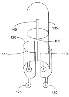
FIGURE 1 illustrates a plasma source chamber with two sets of
antenna elements;
FIGURE 2 illustrates a tunable circuit with an RF power source coupled
to an antenna;
FIGURE 3 illustrates a second tunable circuit with an RF power source
coupled to an antenna;
FIGURE 4 illustrates a third tunable circuit with an RF power source
coupled to an antenna;
FIGURE 5 illustrates a circuit with an RF power amplifier coupled to an
antenna current strap;
14
CA 02529794 2005-12-19
WO 2004/114461 PCT/US2004/019931
FIGURE 6 illustrates a second circuit with an RF power amplifier
coupled to an antenna current strap;
FIGURE 7 illustrates a third circuit with an RF power amplifier coupled
to an antenna current strap;
FIGURE 8 illustrates a simplified model of the RF power amplifier,
antenna current strap, and plasma;
FIGURE 9 illustrates a lumped circuit equivalent of the model depicted
in FIGURE 8;
FIGURE 10 illustrates the frequency response of a plasma source
without a plasma;
FIGURE 11 illustrates the frequency response of a plasma source with
a plasma present;
FIGURE 12 illustrates a feedback arrangement for controlling a plasma
source.
FIGURE 13 illustrates a reactive network for coupling an RF power
source to a plasma; and
FIGURE 14 shows an illustrative embodiment of the invention with
elements selected in a reactive network to eliminate the need for a dynamic
matching network.
CA 02529794 2005-12-19
WO 2004/114461 PCT/US2004/019931
DETAILED DESCRIPTION OF THE INVENTION
Turning to the figures, FIGURE 1 illustrates a plasma source chamber
with two sets of antenna elements. The antenna design includes two
orthogonal single- or multi-turn loop elements 105, 110, 115, and 120,
arranged about a common axis. The antenna elements 105, 110, 115, and
120 are each driven by RF power sources, A 125 or B 130 as shown. Each
antenna loop may be coupled to the same RF power source with a phase
splitter, or to distinct RF power sources, to drive the antenna elements in
quadrature. Preferably the loops in the antenna are constructed from eight (8)
gauge teflon coated wire although bare copper wire or other conductors may
also be used.
FIGURE 1 shows two orthogonal sets of two-element Helmholtz-coil-
like loop antennas, with loop elements 105 and 115 in one set and loop
elements 110 and 120 in the second set. The loop elements are wrapped
azimuthally around an insulating cylinder 135 such that the magnetic fields
that are produced when a current is passed through them are approximately
transverse to the axis of the cylinder. The opposing elements of each set are
connected in series, in a Helmholtz configuration. The wires interconnecting
opposing loop elements are preferably arranged such that adjacent segments
carry currents flowing in opposite directions in order to enhance cancellation
of stray fields associated with them, although this is not necessary to the
device operation. The antennas are energized such that the currents in both
orthogonal branches are nearly equal and phased 90 degrees apart to
produce an approximation to a rotating transverse magnetic field.
16
CA 02529794 2005-12-19
WO 2004/114461 PCT/US2004/019931
In the example case of a helicon mode plasma, a static axial Bo field
140 is produced, for instance, by a simple electromagnet. This field runs
along the axis of the cylinder. The direction of this static field is such
that the
rotating transverse field mimics that of the m = +1 helicon wave. In practice,
the amplitude and direction of the current producing the external field may be
adjusted to modulate the performance of the plasma generator. The overall
amplitude of the necessary field is typically in the range 10-100 Gauss for
the
parameters discussed here, but for different size sources alternative ranges
may be employed. Once the static field optimum amplitude and direction are
chosen, they typically need no further adjustment.
In combination, the static field and the RF field of the antenna elements
produce the m = +1 helicon mode in the plasma inside the insulating cylinder,
which sustains the plasma discharge. It should be noted that it is also
possible to vary, and thus de-tune the static magnetic field, or to not apply
the
field at all, so that the helicon mode is not directly excited. This operation
produces a plasma as well, but typically not as efficiently as the helicon
mode.
Of course, the static field may then be applied to improve the operation of
the
plasma source/generator.
It should also be noted that it is possible to achieve the same overall
conditions of FIGURE 1 using for instance multi-turn loop antennas instead of
single loop, and/or a squat bell jar. Although not a requirement, it is
preferable for the Bell jar to fit within the antenna frame with no more than
a
1 /2" gap.
17
CA 02529794 2005-12-19
WO 2004/114461 PCT/US2004/019931
One example plasma source setup is as follows: A quartz bell jar has
approximately 12" inside diameter (such as a standard K.J. Lesker 12 x 12),
consisting of a straight-cylindrical section approximately 15 cm tall with a
6"
radius hemispherical top. The jar rests atop a vacuum chamber
approximately 12" i.d. x 8" tall (not part of the plasma source). The antennas
consist of two sets of opposing, close-packed, approximately rectangular, two-
turn continuous loop antenna elements that surround the bell jar, with
approximately 1/8" to 1/2" spacing between the antennas and the bell jar at
every point. The turns within each element are connected in series, and the
two elements within each set are also connected in series, such that their
fields are additive. The self-inductance of each set is approximately 10
microHenries in this example, and the mutual inductance between the two
sets is less than 1 microHenry. Vertical and horizontal antenna loop sections
approximately 25cm and 20 cm long, respectively, consist of 8-guage Teflon-
coated wire. In alternative embodiments single turns of rigid copper
conductors may be employed in place of one or two turns of Teflon-coated
wire. The particular embodiments described herein for producing a
transverse rotating field should not be interpreted to limit the scope of the
claimed invention in the absence of express indications.
A conventional RF power source and dynamic matching scheme, see
FIGURES 2 to 4, may be used to excite the antenna currents in the antenna
described above. Moreover, the circuits of FIGURES 2 to 4 are compatible
with many of the disclosed methods. Some of these methods include steps
such as providing a low output impedance to an RF power source; and
adjusting a reactance coupling the RF power source to the antenna such that
18
CA 02529794 2005-12-19
WO 2004/114461 PCT/US2004/019931
the resonance frequency in the absence of a plasma is the desired RF
frequency. A low output impedance can be understood by reference to the
quality factor ("Q") for the circuit with and without the plasma. The "Q" with
no
plasma present should be five to ten-fold or even higher than in the presence
of the plasma. Notably, unlike known circuits, such a combination of the RF
power source and antenna will not need to be readjusted in the presence of
plasma by changing the reactance in response to changes in the plasma
impedance.
In FIGURE 2 the RF source 200 may be a commercial 2 MHz, 0-1 kW
generator, connected to the quadrature/hybrid circuit at port "A" 125
illustrated
in FIGURE 1 via 50 ohm coax. The "+45 degree" and "- 45 degree" legs of
the quadrature/hybrid circuit are connected to individual L-type capacitative
matching networks composed of adjustable capacitors 205, 210, 215, and 220
as shown. The reactance of capacitors 225 is about 100 ohms each at the
operating frequency, and the reactance of either side of the transformer 230
is
about 100 ohms with the other side open. As shown in FIGURE 2, a single
RF source 200 may be used, together with a passive power splitter (the
quadrature/hybrid circuit) and four adjustable tuning elements 205, 210, 215,
and 220 to match to the two separate antenna inductances 235 and 240.
Another embodiment, illustrated in FIGURE 3, employs two separate
RF power sources 305 and 310, and thus entirely separates the two antenna
power circuits connected to inductances 335 and 340 via tunable capacitors
315, 320, 325, and 330 respectively. Such an arrangement is advantageous
in that each RF source can be operated at full power, thus doubling the
19
CA 02529794 2005-12-19
WO 2004/114461 PCT/US2004/019931
amount of input power as compared to that of a single RF source, and the
phasing and amplitude ratio may be adjusted between the antennas.
Typically, sources 305 and 310 are operated at roughly the same amplitude
and at 90 degrees out of phase, although the amplitude and/or phase
difference might be varied in order to change the nature of the excited mode.
For example, by operating them at different amplitudes, an elliptically
polarized plasma helicon mode rather than a strictly circularly polarized mode
could be sustained.
A third embodiment, illustrated in FIGURE 4, places a passive resonant
circuit, comprising inductor/antenna inductance 405 and adjustable capacitor
410 on one leg, and drives the other leg with an RF source 400 with a
dynamic matching circuit having tunable capacitors 415 and 420 connected to
antenna inductance 425. This arrangement tends to excite the same sort of
elliptical helicon mode in the plasma, with the passive side operating
approximately 90 degrees out of phase with the driven side, thus providing
many advantages but with only a single RF source and dynamic matching
network.
The working gas in this example setup is Argon, with pressure ranging
from 10 mTorr to over 100 mTorr. A static axial field is manually settable to
0
- 1506 and is produced by a coil situated outside the bell jar/antenna
assembly, with a radius of about 9".
Plasma operation at a pressure of approximately 75 mTorr exhibits at
least three distinct modes. First, a bright mode in which the plasma is
concentrated near the edge of the bell jar is observed for Bo < B~~,t~m when
PRF
CA 02529794 2005-12-19
WO 2004/114461 PCT/US2004/019931
is less than or approximately 200W. Here, Bo is the axial magnetic field while
B~r~t~m is a critical value for the axial field for exciting a plasma using a
helicon
mode. Similarly, power levels PRF and P~,,resno~d denote the RF power supplied
to the antenna and a threshold power described below. In this mode, the RF
antenna currents tend to not be in quadrature, instead being as much as 180
degrees out of phase. Second, a dull-glow-discharge-like mode, with uniform
density/glow at higher power but with approximately 1-2cm thick dark space
along the wall of the bell jar at lower powers, is observed for Bo > B~~~t~m
but
PRF ~ Pthreshold~ In this case the RF currents are in robust quadrature,
appearing to abruptly lock at approximately 90 degrees phase shift shortly
after the plasma is formed. Third, at higher PRF > Ptnresno~d and with Bo >
B~r~t~~i, a bright plasma is formed that appears to be more evenly radially
distributed than that of mode (1 ), and the antenna currents again tend to
lock
into quadrature phasing. The third regime represents an efficient mode of
operation, and can be achieved at a neutral gas pressure that has proven to
be very difficult to access for known plasma sources, although each of these
regimes may have application in plasma processing.
In an aspect, the conventional RF power source and tunable matching
network described in FIGURES 2 to 4may be eliminated in favor of a
streamlined power circuit.
In a preferred embodiment, an RF power circuit drives the antenna
current strap directly, using an arrangement such as that shown in FIGURE 5.
The RF amplifier illustrated in FIGURE 5 is preferably one of the many types
of RF amplifiers having a low output impedance (i.e. a push-pull output stage)
21
CA 02529794 2005-12-19
WO 2004/114461 PCT/US2004/019931
that are known in the field. Transistors 505 and 510 are driven in a push-pull
arrangement by appropriate circuitry 500, as is known to one of ordinary skill
in the art. In this arrangement typically one transistor is conducting at any
time, typically with a duty cycle of or less than 50%. The output of the the
transistors is combined to generate the complete signal.
Preferably, the power semiconductors, e.g., transistors 505 and 510, in
the output stage are operated in switching mode. In the FIGURES 5-7 these
are depicted as FETs, but they can also be, for example, bipolar transistors,
IGBTs, vacuum tubes, or any other suitable amplifying device. An example of
switching mode operations is provided by Class D amplifier operation. In this
mode alternate output devices are rapidly switched on and off on opposite
half-cycles of the RF waveform. Ideally since the output devices are either
completely ON with zero voltage drop, or completely OFF with no current flow
there should be no power dissipation. Consequently class D operation is
ideally capable of 100% efficiency. However, this estimate assumes zero ON-
impedance switches with infinitely fast switching times. Actual
implementations typically exhibit efficiencies approaching 90%.
Preferably, the RF driver is coupled directly to the antenna current
strap 520 through a fixed or variable reactance 515, preferably a capacitor.
This coupling reactance value is preferably such'that the resonant frequency
of the circuit with the coupling reactance and the antenna, with no plasma
present, is approximately equal to the RF operating frequency.
An alternative arrangement of the output stage of this circuit, illustrated
in FIGURE 6 (A), includes a transformer 620 following or incorporated into the
22
CA 02529794 2005-12-19
WO 2004/114461 PCT/US2004/019931
push-pull stage, with driver 600 and transistors 605 and 610, to provide
electrical isolation. Transformer 620 may optionally be configured to
transform the output impedance of the push-pull stage, if too high, to a low
impedance. Capacitor 615 is arranged to be in resonance at the desired drive
frequency with the inductive circuit formed by transformer 620 and antenna
current strap 625. A similar embodiment is shown in FIGURE 6(B), where
capacitor 615 is used for DC elimination, and capacitor 630 is resonant in the
series circuit formed by leakage inductance of transformer 620 and
inductance of the current strap 625.
FIGURE 7 illustrates yet another RF power and antenna current strap
configuration. A center-tapped inductor 725 incorporated in the DC power
feed is connected to the output stage having push-pull driver 700 and
transistors 705 and 710. Isolation is provided by transformer 720. Again, only
one or the other transistor is conducting at any time, typically with a duty
cycle
of less than 50%. The circuits of FIGURES 5-7 are provided as illustrative
examples only. Any well-known push-pull stage or other configurations
providing a low output impedance may be used in their place.
The RF power source may also be used with any helicon antenna,
such as either a symmetric (Nagoya Type III or variation thereof, e.g.,
Boswell-type paddle-shaped antenna) or asymmetric (e.g., right-hand helical,
twisted-Nagoya-III antenna) antenna configuration, or any other non-helicon
inductively coupled configuration.
The RF power source may be amplitude modulated with a variable duty
cycle to provide times of reduced or zero plasma density interspersed with
23
CA 02529794 2005-12-19
WO 2004/114461 PCT/US2004/019931
times of higher plasma density. This modulation of the plasma density can be
used to affect the flow dynamics and uniformity of the working gas, and
consequently the uniformity of the process. A more spatially uniform
distribution comprising plasma may therefore be generated by a plasma
generator system by a suitable choice of a modulation scheme.
In general, a plasma generator system may use radio frequency power
sources based on operation as a substantially Class A amplifier, a
substantially Class AB amplifier, a substantially Class B amplifier, a
substantially Class C amplifier, a substantially Class D amplifier, a
substantially Class E amplifier, or a substantially Class F amplifier or any
sub-
combination thereof. Such power sources in further combination with the
antennas for exciting helicon mode are suitable for generating high density
plasmas. Moreover, for non-switching amplifiers, such as those shown in
FIGURES 2-4, an intermediate stage to transform the RF source impedance
to a low output impedance may be employed to approximate the efficient
operation of the switching amplifier based embodiments described herein.
In inductively coupled plasma sources, the antenna current strap is
located in proximity to the region where plasma is formed, usually outside of
an insulating vessel. From a circuit point of view, the antenna element forms
the primary of a non-ideal transformer, with the plasma being the secondary.
An equivalent circuit is shown in FIGURE 8, in which inductor 810 represents
a lumped-element representation of the current strap and any inductance in
the wiring, including any inductance added by e.g., the driver's output
transformer present in some embodiments. Components in the box labeled P
24
CA 02529794 2005-12-19
WO 2004/114461 PCT/US2004/019931
represent the plasma: inductor 820 is the plasma self inductance, and
impedance 815 represents the plasma dissipation, modeled as an effective
resistance. M represents the mutual inductance between the antenna and
plasma. Transistor driver 800 is represented as a square-wave voltage
source. The capacitance 805 is adjusted at the time the system is installed to
make the resonant frequency of the circuit approximately match the desired
operating frequency. In an alternate embodiment with a fixed capacitor, the
RF frequency may be adjusted to achieve the same effect.
For illustrating the operation of the system, the overall system may be
modeled as shown in FIGURE 9. In FIGURE 9 all inductors have been
lumped into inductance 905, all capacitors into capacitance 910, and all
dissipating elements into resistor 915, and the amplifier should ideally
operate
as an RF voltage source (i.e., having zero output impedance).
With no plasma present, R is small since there is little dissipation, and
the circuit of FIGURE 9 exhibits a narrow resonant response to changes in
frequency, as shown in FIGURE 10. This provides one of the advantages of
the circuit's operation: it is possible to drive the voltage on the antenna to
a
high value with relatively little power input, thus facilitating the initial
breakdown of the gas in the reaction chamber. Once the plasma forms, the
damping in the system considerably broadens the resonant peak, as shown in
FIGURE 11, reducing the Q of the overall circuit. Although the center
frequency of the resonance may shift with plasma conditions, that shift is
negligible compared to the width of the resonant response when the plasma
load is present. Therefore, when operating with a plasma load the circuit is
CA 02529794 2005-12-19
WO 2004/114461 PCT/US2004/019931
relatively insensitive to variations in operating conditions, and requires no
retuning. This is illustrated in FIGURE 11, where the overall system
resonance has shifted its frequency slightly, although the Q is sufficiently
reduced that the operation of the system remains efficient. With the reduced
Q of the circuit, the voltage applied to the plasma self-adjusts to be
considerably reduced over the no-plasma case. In some embodiments, it
may be somewhat advantageous to actually detune the operating frequency
of the RF drive slightly from the exact no-plasma resonance to one side or the
other, depending on the shift of the resonant frequency when the plasma
forms.
The level of power input to the plasma may be controlled by a variety of
techniques, such as adjusting the DC supply level on the RF output stage. In
one embodiment, the supply voltage may be in response to sensed variations
in plasma loading to maintain a relatively constant power into the plasma
source. As illustrated in FIGURE 12, the sensing of plasma loading for
adjustments by DC supply regulator 1230 may be achieved, for example, by
monitoring the voltage from the DC supply 1215 by voltage sensor 1200 and
the DC current into the RF/Plasma system by current sensor 1205, and using
their product together with a previously measured approximation to the
amplifier efficiency in module 1210 to estimate the net power into the plasma
1225 from RF Amplifier 1220. Efficiency multiplier for gain module 1235 can
be measured for different output levels, for instance by monitoring heat loads
at various points of the system, and stored digitally, so that variations in
efficiency with output level are accounted for. Alternatively, the RF voltage
26
CA 02529794 2005-12-19
WO 2004/114461 PCT/US2004/019931
and current can be measured, and their in-phase product evaluated to
estimate the real power being dissipated in the plasma.
The sensing of plasma may also extend to sensing spatial uniformity by
either direct sensing or indirect sensing by way of variations in the voltage
or
current. Changing the duty cycle in response to such variations can then
control the spatial distribution of plasma. In addition, modulating the duty
cycle can further allow control over the average input power to improve the
efficiency of plasma generation. The feedback arrangement of FIGURE 12
can also allow switching between two or more power levels as described
previously.
"Low" impedance, as used herein, means that the series resonant
circuit shown in FIGURE 9 has a "Q" that should be five to ten-fold or even
higher with no plasma present than with plasma present. That is, the amplifier
output impedance should be sufficiently small that the energy dissipated in a
half-cycle of output is much less than that stored in the reactive components.
This condition is mathematically defined as Zo"t « ~ , where L and C are
the lumped values shown in FIGURE 9. The RF amplifier will approach
operation as a voltage source when this condition holds.
A low resistance, e.g., for the output impedance of the RF source,
generally refers to a resistance of less than about 10 ohm, preferably less
than about 6 Ohms, more preferably less than about 4 Ohms, and most
preferably less than about 1 Ohm.
27
CA 02529794 2005-12-19
WO 2004/114461 PCT/US2004/019931
However, not all embodiments of the invention require that the
elements in the reactive circuit coupling the RF power source to the
antenna/plasma be selected based on the resonant frequency of the circuit
without a plasma being present. Indeed several, alternative conditions are
possible that allow a suitable specification of the reactive circuit such that
there is no need for a dynamic matching circuit while efficient coupling is
possible with the dynamic impedance of a plasma.
While presenting a variable impedance, it is possible to describe the
plasma reactance as being expected to be confined between a high and a low
limit. Thus, a high expected plasma reactance component and a low
expected plasma reactance may be specified. For instance, such a
specification may reflect a one-Q distance away from the expected mean
value. Many other similar specifications are possible to indicate the
likelihood
of the plasma impedance actually falling outside the specified limits. Indeed,
instead of a high expected plasma reactance, it is possible to specify a value
that is not symmetrically placed relative to the low expected plasma
reactance. Moreover, while a particular plasma impedance may fail to
conform to a normal distribution, a collection of several plasmas is likely to
collectively present a normal distribution for the combined impedance.
Similarly, a collection of several RF power sources connected together
is likely to exhibit a normal distribution, both with respect to frequency and
time. Then a suitable choice of a reactance network may actually ensure that
the variation in plasma reactance is well matched to the variation in the RF
28
CA 02529794 2005-12-19
WO 2004/114461 PCT/US2004/019931
power sources by matching them at two values of the expected plasma
reactance.
With such a specification of the plasma reactance and a knowledge or
estimate of the lowest or likely low plasma resistance, a value at which the
variation of the plasma impedance is likely to be the greatest, it is possible
to
arrive at a method of specifying the components in the reactive circuit.
For example, in the illustrative circuit of FIGURE 13, from the
publication "3kW and 5 kW Half-bridge Class-D RF Generators at 13.56MHz
with 89% Efficiency and and Limited Frequency Agility", Directed Energy Inc.
~ 2002, document number 9300-0008 Rev. 1," retrieved on June 10, 2004
from the web address
http://www.ixysrf.com/pdf/switch_mode/appnotes/3ap_3 5kw13_56mhz gen.
pdf, which is incorporated herein by reference, with the specification that
the
impedance at the RF jack is 50 Ohms, Ca=C~+C2, and Cb=C3+Ca, the series
impedance is Z~= 1 +sL, -1+szL,C~ , and shunt impedance
sCa sCa
ZL
Z2 sCb 1 1+ ZL C ' The impedance seen at the input is Z~+Z2. With L1
ZL + L b
sCb
given as 2.1 NH, this complex value may be adjusted with suitable
components to be 14 +i12.6 Ohms by adjusting Ca to be about 81.6 pF and Cb
at about 376 pF.
In a capacitively coupled system, e.g. for use at 13.56 MHz to provide
an RF bias for a substrate in a semiconductor processing chamber, an
29
CA 02529794 2005-12-19
WO 2004/114461 PCT/US2004/019931
illustrative plasma antenna combination may, for example, present a
resistance Rp of about 1 to 4 Ohms and a reactance Xp of about -8 to -25
Ohms. Thus, hooking the circuit of Figure 13 to such an antenna/plasma
combination is difficult in general. With the large imaginary component of the
impedance that it sees, the transistor switching circuit will safely operate
with
a supply voltage that is a fraction of the desired peak supply voltage of
about
700 to 800 V, e.g., at about 250 V (more likely 200). The peak output voltage
is given by VS"Pp~y/2 X Phil, where ~H~ is the magnitude of the transfer
function
of the system, and in the 250 V case will range from about 28 to 83 V for the
various plasma conditions.
when operating at a given frequency, a total impedance may be
adjusted by adding an inductor (having a positive reactance) or a capacitor
(having a negative reactance) in series with the impedance. As an example, if
there is a stray inductance L due e.g. to leads and the like, the total
impedance may be adjusted to a level at or near zero for a given operating
frequency by adding a capacitor in series, with the capacitance adjusted so
that Ztot = Z~+Zc =i~L- 1 ~ 0 . Similarly, in driver circuits using output
i f.~C
devices with significant output capacitance, such as transistors or mosfets,
dissipation due to the output capacitance (e.g. CosS on some specification
sheets) may be reduced by providing a slightly inductive load. This is
because of the charge stored in the capacitance: a properly tuned inductive
load discharges the capacitance without having to dissipate this charge.
FIGURE 14 shows an illustrative general reactive circuit 1400 suitable
for coupling radiofrequency power source 1405 to a capacitively driven
CA 02529794 2005-12-19
WO 2004/114461 PCT/US2004/019931
plasma or an antenna-plasma combination. Although, this circuit relates to a
capacitively coupled driver, e.g., for the RF biasing of a substrate in a
semiconductor processing plasma, but the principle for determining the values
of the components applies to an inductively coupled system as well. The
illustrative general reactive circuit 1400 may be tuned either using the
capacitors or inductors or both. For instance, the reactance of capacitors
1415 and 1425 may be chosen to be approximately the same as the minimum
plasma reactive component, at about 500 pF each. Inductors 1410 and 1420
are then tuned to satisfy two conditions: a) at the largest magnitude of
plasma
reactance, i.e., a high expected plasma reactance limit, the imaginary part of
the overall load seen by the transistor output stage is small, and b) at the
smallest magnitude of plasma reactance, i.e., a low expected plasma
reactance limit, the imaginary part of the load seen by the output stage is
adjusted to optimize operation of the radio frequency power source, e.g., +12
Ohms as in the circuit described in the above Directed Energy reference.
The impedance seen by a transistor driver stage is given by Z~oad =
21410 + 21415 + (21420 ~' Z1425)IIZp~ Here Z~a~o represents the impedance of
inductor 1410 in FIGURE 14 and the like while ZP represents one value of
expected plasma reactance. That is, the driver sees capacitor 1410 in series
with inductor 1415 and in series with the parallel combination of plasma
impedance 1440 and capacitor 1425 + inductor 1420 series combination.
For a radio frequency power source, which operates best when it
drives load with a with an output reactance of +12 Ohms, case "a"
corresponds to Im(Z,oad) of about 0 Ohms at a plasma reactance, Xp, of about
31
CA 02529794 2005-12-19
WO 2004/114461 PCT/US2004/019931
-25 Ohms. Case "b," then corresponds to Im(Z~oaa) being about 12 Ohms at
Xp of about -8 Ohms. These conditions result in a pair of equations that may
be solved with Rp set at a low value, say about 1 Ohm, since this level of
plasma resistance results in large variations in the load seen by the RF
driver.
These two equations can be solved for the unknown value of inductances
1415 and 1420. Under the described conditions, in this exemplary
embodiment, values of inductance 1420 is about 345 nH and inductance 1415
is about 185 nH resulting in Im(Z,oad) of about 0 Ohms for condition "a" and
Im(Zioad) of about 11.9 Ohms for condition "b"' respectively. More
sophisticated calculations preferably take into account stray inductances,
coil
inductances and the like along with other non-ideal effects.
Alternative choices may be elected for the value for capacitors 1410
and 1425, e.g., by electing smaller values to improve the tolerance if
subtracting two comparable numbers is resulting in large errors. Additionally,
instead of fixing the values for capacitors 1410 and 1425, and adjusting the
values for inductors 1415 and 1420, it is also possible to fix the value for
inductors 1415 and 1420 and adjust the value of capacitors 1410 and 1425.
It will be recognized further that the total impedance is the important
quantity
for any series or parallel combination of reactive components, and that
specific values of L and C or specific geometries can be used in the above
circuit. As an example, a series combination of an inductor L and a capacitor
C can have a reactance of about 5.9 ohms when L=345 nH and C=500 pF, or
when L= 620.5 nH and C=250 pF. These values can be adjusted to satisfy
other constraints in the system, such as the need to have a high (or low)
impedance at a 2"d harmonic.
32
CA 02529794 2005-12-19
WO 2004/114461 PCT/US2004/019931
Alternative output transistor stages may be operated at different
impedances in the reactive load, including a slightly capacitive load. Then,
the condition Im(Zioad) is about 0 Ohms may be specified at some midpoint
value rather than for the low or high expected plasma reactance limit. Thus,
at this specified magnitude of plasma reactance, i.e., a specified plasma
reactance limit, the imaginary part of the overall load seen by the transistor
output stage is small. Further, the specified plasma reactance may be a value
outside the range of expected operation. However, such a specification may
result in higher output current. In addition, adding a resistive path in
parallel
with capacitor 1425 improves the performance of the reactive circuit. Thus,
the reactive circuit may include resistive elements as well.
In another aspect, nonlinear resistive or reactive elements may be
used for the purpose of reducing the impedance variation seen by the RF
power source. In yet another aspect, the inductors 1415 and 1420 may be
arranged to have a small amount of mutual inductance, which can be either
positive or negative. A positive mutual inductance M~4~5,1420, e.g., in the
range
M1415,1420 ~ 0.02, may be used to reduce the sensitivity of the response
LiaisLia2o
transfer function H to changes in plasma reactance, while negative mutual
inductance may increase the sensitivity.
These methods for tuning or setting up of a reactive network provide
several advantages in addition to removing the need for a dynamically tuned
matching circuit. For example, since the tuning at one plasma reactance in
the range of reactance values expected for a plasma matches that for the
33
CA 02529794 2005-12-19
WO 2004/114461 PCT/US2004/019931
operation of amplifier, it provides the transistors with the reactive
impedance
needed for efficiently operating at a high voltage. Further, although at the
other end of the plasma range, the reactance seen by the output stage is
small, the total load is also small, enabling operation at high current and
low
supply voltage resulting in the reactance presented to the transistors being
less important. Moreover, this specification ensures that over a broad range
of plasma reactance, a reasonable amount of power may be delivered from
the RF source to the plasma. In another aspect, with this design enables use
of a large number of output stages that may be combined, for instance, in
parallel.
Often the specification for a RF power supply is an output voltage for
application to the antenna terminals, with the RF input voltage level being
adjusted to produce this desired output voltage according to what is
necessary for varying plasma operating conditions. Examination of the
transfer function H = Vp~asma ~ Vin reveals that the system "voltage transfer
function," or the ratio of output voltage to input voltage, H = Vplasma ~ V~~
_ [
(Z1410 + z1415)IIZp J ~ Zload~
For the tuning as described, this transfer function has a resonant
character, in that the magnitude of H is greater than one over a substantial,
if
not the entire, range of operation. ~H~ varies from approximately 75 at Xp of
about -25 Ohms (case "a" above, with Rp of about 1 Ohm) down to
approximately 1.5 at Xp = -8 Ohms (case "b" above, with Rp still at about 1
Ohm). For the higher plasma resistance, for instance, Rp of about 4 Ohms,
~H~ varies from approximately 21 to 1.6. Therefore, selecting a reactance
34
CA 02529794 2005-12-19
WO 2004/114461 PCT/US2004/019931
network well suited for operation at the lowest expected plasma resistance
ensures with high degree of certainty that the variation in plasma impedance
would be smaller at a higher values of the plasma resistance.
It should be noted that although some of the discussion is in terms of
the resonant frequencies for the reactive network, it is often desirable to
drive
the radio frequency power source at a frequency that deviates somewhat from
the resonant frequency in the absence of a plasma in the direction of the
frequency spread due to the presence of the plasma. This ensures stable and
efficient operation over frequencies of interest.
The disclosed system and methods provide an advantage in being able
to break down this gas and initiate the plasma by virtue of the fact that the
high Q of the circuit with no plasma allows high voltages to be induced on the
antenna element with relatively low power requirements. This no-plasma
voltage can be controlled to give a programmed breakdown of the working
gas; once the plasma forms, induced currents in the plasma serve to load the
system and lower the high voltages for inducing the breakdown, and thus,
avoid stressing the system.
The described circuit arrangements do not require a variable tuning
element, such as a mechanically adjustable capacitor, since only fixed
capacitance C is necessary. However, the various circuits can also be
constructed using a variable capacitor that is adjusted, for example, for
matching of the system resonance to the desired operating frequency, in a
preferred embodiment, and is not needed for real-time impedance matching
with the plasma operating point. Such matching is useful to counter the
CA 02529794 2005-12-19
WO 2004/114461 PCT/US2004/019931
effects of mechanical vibration or aging that may cause the L-C resonant
frequency to drift.
In one embodiment, the operating frequency is adjusted to compensate
for small deviations from resonance, while mechanically tuning the capacitor
compensates for large deviations. In an alternative embodiment, adjustments
are made by tuning the capacitor. In the preferred (tuned) embodiment, this
tuning is automated and takes place during periods when the source is off-
line. In another aspect, with tuning as part of the process control, for
instance
to provide small tweaks to the process conditions, the disclosed arrangement
reduces the number of adjustable elements to as few as one in embodiments
with adjustable tuning elements.
As one skilled in the art will appreciate, the disclosed invention is
susceptible to many variations and alternative implementations without
departing from its teachings or spirit. Such modifications are intended to be
within the scope of the claims appended below. For instance, one may
provide impedance matching for a low impedance with a transformer in
combination with a conventional amplifier. Also, although the invention
obviates the need for dynamic matching circuits, the use of some dynamic
matching circuit in combination with the reactive circuits disclosed herein to
reduce the otherwise stringent requirements placed on dynamic matching
networks is intended to be included within the scope of the invention as
indicated. Therefore, the claims must be read to cover such modifications
and variations and their equivalents. Moreover, all references cited herein
are
incorporated by reference in their entirety for their disclosure and
teachings.
36