Note: Descriptions are shown in the official language in which they were submitted.
CA 02530115 2011-07-28
Alarm Test and Reset
The present invention relates to an alarm and particularly, but not
exclusively, to
an improved form of mains-powered smoke alarm.
Until recently, smoke alarms and other types of alarms for detecting
radiation,
heat and air pollutants or the like, were relatively bulky devices powered
only by
= means of a battery. No provision for recharging the battery was included
and thus
correct operation of the alarm required the regular changing of the battery to
ensure the alarm remained powered. Owing to an increasing awareness of the
need for such alarms in domestic buildings and offices, it has become common
to
provide alarms which are mains-powered and which include a rechargeable
battery for powering the alarm in the event that mains power is disrupted.
An improvement to general mains powered smoke alarms are alarms which can
be connected to a lighting circuit. International Patent Application
publication No.
W000/21407 discloses an alarm for detecting radiation and/or pollutants such
as
smoke, carbon monoxide or the like which is arranged to interconnect between a
light fitting and a light source such as a bulb. The alarm is powered by the
light
fitting when the light fitting is energised and is powered by a battery when
the
light fitting is de-energised.
International Patent Application publication No. WO 00/58924 discloses an
alarm
for detecting radiation and/or pollutants such as smoke, carbon monoxide,
methane, radon or the like comprising a housing which is intended to replace a
ceiling rose for a light fitting.
The above described devices permit relatively easy installation to existing
lighting
circuits but suffer the disadvantage that a light fitting, such as a batten or
pendant
ceiling fitting, is required for such installation. It is difficult or
impossible to install
such devices at locations in a building where there are no light fittings.
Building
regulations currently often require that mains-powered alarms be fitted at
specific
1
CA 02530115 2005-12-20
WO 2004/001692 PCT/GB2003/002714
areas within buildings which may not coincide with the position of light
fittings.
It is an aim of the present invention to provide an improved mains-powered
alarm
connectable in a lighting circuit or other mains circuit. It is a further aim
of the
invention to provide an alarm which is more easily installed and which does
not
require to be fitted in conjunction with a light fitting.
The present invention provides an alarm for detecting radiation and/or
pollutants
such as smoke, carbon monoxide or the like having: a housing means; an alarm
circuit including detection means for detecting said radiation and/or
pollutants;
first electrical connection means connectable to an external power supply for
supplying power to said alarm circuit; and control means responsive to receipt
of
a preselected number of pulses over a preselected time period to apply a
preset
control signal to said alarm circuit; wherein said alarm circuit is responsive
to said
preset control signal to reset or test said alarm in dependence on said preset
control signal.
In a preferred form of the invention said control means is responsive to the
energising and de-energising of the external power supply said preselected
number of times over said preselected time period to apply said preset control
signal to said alarm circuit. Said alarm has first switch means actuable by a
user
to generate a respective pulse for each actuation thereby to apply a user
selected
number of pulses to said control means; and said control means is responsive
to
receipt of said preselected number of said pulses over said preselected time
period to apply a preset control signal to said alarm circuit.
Preferably, said first switch means is mounted on said alarm housing.
Preferably, said first switch means is mounted remote from said alarm housing.
Preferably, said first switch means is adapted for connection to a switch live
side
of a switch for a lighting circuit.
2
CA 02530115 2005-12-20
WO 2004/001692 PCT/GB2003/002714
Preferably, said alarm has second electrical connection means for connection
to
a switch live side of a switch for a lighting circuit; and wherein said second
electrical connection means is operable to receive pulses caused by user
actuation of said switch between its on and off states and apply said pulses
to
said control means thereby to cause a preset control signal to be applied to
said
alarm circuit in response to generation of said preselected number of pulses
over
said preselected time period,.
Preferably, switch means for an external light source are provided and are
actuable in response to generation of a preselected control signal to energise
said light source.
Preferably, the alarm comprises a relay and a light source wherein said relay
is
actuable in response to generation of a preselected control signal to energise
said light source.
Preferably, when said preselected number of pulses over said preselected time
period is one, said control means is operable to apply a preset control signal
to
said alarm circuit thereby to reset said alarm.
Preferably, when said preselected number of pulses over said preselected time
period is one, said control means is operable to apply a preset control signal
to
said alarm circuit thereby to test said alarm.
Preferably, when said preselected number of pulses over said preselected time
period is two, said control means is operable to apply a preset control signal
to
said alarm circuit thereby to test said alarm.
Preferably, when said preselected number of pulses over said preselected time
period is two, said control means is operable to apply a preset control signal
to
said alarm circuit thereby to reset said alarm.
3
CA 02530115 2005-12-20
WO 2004/001692 PCT/GB2003/002714
Preferably, said alarm circuit comprises means for reducing the sensitivity of
said
detection means.
operable in response to generation of a reset control signal by said control
means
to reduce the sensitivity of said detection means for a preselected time
period
thereby to reset said alarm.
said detection means.
Preferably, said means for increasing the sensitivity of said detection means
is
operable in response to generation of a test control signal by said control
means
Preferably, the alarm comprises a battery for supplying power to said alarm in
the
absence of mains power; and a charging circuit including said first electrical
Preferably, the alarm comprises isolating means for selectably electrically
disconnecting said battery from said alarm thereby to minimise leakage from
said
Preferably, said isolating means comprises a second switch means in said power
rail switchable between a first, conducting state connecting said battery to
said
alarm and a second, non-conduction state disconnecting said battery from said
30 alarm.
Preferably, said charging circuit comprises a third switch means switchable
4
CA 02530115 2005-12-20
WO 2004/001692 PCT/GB2003/002714
between a first, conducting state and a second, non-conducting state in
dependence on the voltage on said power rail; and wherein: when said third
switch means is in said first, conducting state said third switch means is
operable
to retain said isolating second switch means in its conducting state; and when
said third switch means is in said second, non-conducting state the state of
said
third switch means is dependent on the voltage on said power rail such that
said
second switch means is non-conducting in response to said voltage on said
power rail being below a preselected value indicating a low battery charge,
thereby to disarm said alarm during charging of said battery.
Preferably, the alarm comprises a disconnect means actuable to switch said
switch means into its non-conducting state thereby disabling said switch means
and preventing actuation of said alarm.
Preferably, said disconnect means comprises button means movable between a
first, OFF position wherein said switch means is rendered non-conducting and a
second, ON position wherein said switch means is enabled.
Preferably, said switch means is a multi electrode semiconductor device having
a
control electrode for controlling conduction between further electrodes
thereof;
and said button means is movable into its first, OFF position to vary the
potential
on said control gate means thereby to render said switch means non-conducting.
Preferably, said housing comprises: a first backing plate for mounting on a
surface; a second backing plate detachably mountable on said first backing
plate;
and a cover means for covering said backing plates; and wherein the
arrangement of said disconnect means is such that engagement of said second
backing plate on said first backing plate moves said disconnect means into its
second, ON position thereby to enable said switch means and disengagement of
said second backing plate from said first backing plate moves said disconnect
means into its first, OFF position thereby to disable said switch means.
5
CA 02530115 2005-12-20
WO 2004/001692 PCT/GB2003/002714
Preferably, the alarm comprises indicator means operable in response to power
on said voltage rail downstream of said isolating means to indicate that said
alarm is enabled.
The present invention also provides an alarm for detecting radiation and/or
pollutants such as smoke, carbon monoxide or the like having: a housing means;
an alarm circuit including detection means for detecting said radiation and/or
pollutants; first electrical connection means connectable to an external power
supply for supplying power to said alarm circuit; and switch means for a light
source, said switch means being actuable in response to triggering of said
alarm
to energise said light source.
Preferably, said switch means comprises a relay and said light source is
external
to said alarm.
Preferably, said light source is mounted in said alarm.
The present invention further provides an alarm for detecting radiation and/or
pollutants such as smoke, carbon monoxide or the like having: a housing means;
an alarm circuit including detection means for detecting said radiation and/or
pollutants; first electrical connection means connectable to an external power
supply for supplying power to said alarm circuit; a battery for supplying
power to
said alarm in the absence of mains power; a charging circuit including said
first
electrical connection means for supplying power to a power rail for said alarm
and for charging said battery; and an isolating means for selectably
electrically
disconnecting said battery from said alarm thereby to minimise leakage from
said
battery when said alarm is inactive.
Preferably, said isolating means comprises a second switch means in said power
rail switchable between a first, conducting state connecting said battery to
said
alarm and a second, non-conduction state disconnecting said battery from said
alarm.
6
CA 02530115 2005-12-20
WO 2004/001692 PCT/GB2003/002714
Preferably, said charging circuit comprises a third switch means switchable
between a first, conducting state and a second, non-conducting state in
dependence on the voltage on said power rail; and wherein: when said third
switch means is in said first, conducting state said third switch means is
operable
to retain said isolating second switch means in its conducting state; and when
said third switch means is in said second, non-conducting state the state of
said
third switch means is dependent on the voltage on said power rail such that
said
second switch means is non-conducting in response to said voltage on said
power rail being below a preselected value indicating a low battery charge,
thereby to disarm said alarm during charging of said battery.
Preferably, the alarm comprises a disconnect means actuable to switch said
switch means into its non-conducting state thereby disabling said switch means
and preventing actuation of said alarm.
Preferably, said disconnect means comprises button means movable between a
first, OFF position wherein said switch means is rendered non-conducting and a
second, ON position wherein said switch means is enabled.
Preferably, said switch means is a multi electrode semiconductor device having
a
control electrode for controlling conduction between further electrodes
thereof;
and said button means is movable into its first, OFF position to vary the
potential
on said control gate means thereby to render said switch means non-conducting.
Preferably, said housing comprises: a first backing plate for mounting on a
surface; a second backing plate detachably mountable on said first backing
plate;
and a cover means for covering said backing plates; and wherein the
arrangement of said disconnect means is such that engagement of said second
backing plate on said first backing plate moves said disconnect means into its
second, ON position thereby to enable said switch means and disengagement of
said second backing plate from said first backing plate moves said disconnect
7
CA 02530115 2005-12-20
WO 2004/001692 PCT/GB2003/002714
means into its first, OFF position thereby to disable said switch means.
Preferably, the alarm further comprises indicator means operable in response
to
power on said voltage rail downstream of said isolating means to indicate that
said alarm is enabled.
The present invention will now be described, by way of example only, with
reference to the accompanyhg drawings in which:
Figure 1 is a block circuit diagram of a preferred form of alarm according to
the
invention;
Figure 2 is a schematic circuit diagram of a charging circuit of the alarm of
Figure
1;
Figure 3is a schematic circuit diagram of a disconnect circuit of the alarm of
Figure 1;
Figure 4 is a schematic circuit diagram of a control circuit of the alarm of
Figure 1;
Figure 5 is a schematic circuit diagram of a detection circuit of the alarm of
Figure
1;
Figure 6 is a circuit diagram of an alternative form of charging circuit for
the alarm
of Figure 1;
Figure 7 is a circuit diagram of an alternative form of control circuit for
the alarm
of Figure 1;
Figure 8 is a first perspective view of a housing for the alarm of Figure 1;
Figure 9 is a second perspective view of the housing of Figure 8;
8
CA 02530115 2005-12-20
WO 2004/001692 PCT/GB2003/002714
Figure 10 is a partial section through the alarm of Figure 8;
Figure 11 is a perspective view from above of a mechanical disconnect
mechanism for the disconnect circuit of Figure 3;
Figure 12 is a further perspective view from above of the mechanical
disconnect
mechanism of Figure 11;
Figure 13 is a perspective view from below of part of the mechanical
disconnect
mechanism of Figure 11;
Figure 14 is a perspective view from below of part of the alarm housing
showing
a power socket of the alarm and a socket holder in spaced relationship;
Figure 15 is a perspective view similar to that of Figure 14 showing the power
socket engaged in the socket holder;
Figure 16 is a schematic diagram showing a first method of connection of the
alarm to the consumer wiring system;
Figure 17 is a schematic diagram showing a second method of connection of the
alarm to the consumer wiring system; and
Figure 18 is a schematic diagram showing a third method of connection of the
alarm to the consumer wiring system.
Figure 19 is a block diagram of the circuit of a further form of alarm; and
Figure 20 is a schematic diagram of a power on circuit for the disconnect
circuit
of Figure 3.
9
CA 02530115 2005-12-20
WO 2004/001692 PCT/GB2003/002714
While the following description is made with reference to a smoke alarm, it
will be
understood that the invention is applicable to other types of alarms, such as
those for detecting radiation, air pollutants such as methane, radon or carbon
monoxide, and/or heat or the like. In addition, the term "earth" in the
context of a
It should also be noted that the symbol Vcc is used to indicate a connection
to a
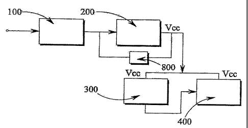
Referring firstly to Figure 1, this shows a block circuit diagram for a
preferred
form of alarm according to the invention. The alarm circuit has a charging
circuit
The charging circuit provides a rectified and smoothed voltage for the control
and
detection circuits 300, 400 whilst the disconnect circuit 200 controls the
The circuits 100 to 800 will be well understood by those skilled in the art
and for
convenience, therefore, only those features of the circuits which are
important for
the understanding (and not necessarily the operation) of the invention are
The charging circuit 100 is shown in detail in Figure 2 and includes first and
second inputs PL1, PL2 for connection to the live and neutral cables of an AC
power supply. In the illustrated embodiment, the AC power supply is formed by
CA 02530115 2011-07-28
charging circuit 100 when the light is switched on. The phrase "switched live"
as
used herein refers to the cable which connects the light switch of the
lighting
circuit to a lamp of the circuit such that when the switch is closed, power is
applied through the cable to the lamp.
The first and second inputs PL1, PL2 of the charging circuit are connected to
respeCtive inputs of a diode rectifier or rectifier bridge BR1 which serves to
apply
full-wave rectification to the AC volthge, thereby generating a DC voltage.
The outputs of the rectifier bridge BR1 form positive and earth rails 110, 112
for
the charging circuit 100. The rectified DC voltage is applied to the positive
rail
110 and a smoothing capacitor C2 is connected between the positive and earth
rails 110; 112 for smoothing the DC current from the rectifier bridge BR1. A
Zener diode D2 is reverse biased across the positive and earth rails 110, 112
for
clipping the voltage output of the rectifier bridge BR1 and hence isolating
the
further circuitry in the charging circuit from voltage spikes on the power
supply.
= The DC voltage from the bridge rectifier BR1 is applied to the input of a
voltage
regulator ICI which serves to regulate the voltage. The output of the voltage
regulator forms a charging rail 111 and the reference input of the voltage
regulator is connected to the junction between two reference resistors R7, R8,
connected in series between the charging rail 111 and the earth rail 112.
The charging circuit further includes a switch in the form of a transistor TR5
whose collector is connected to the charging rail 111 via a resistor R31. The
emitter of the transistor TR5 is connected to the earth rail 112 and the base
is
connected to a potential divider formed by two resistors R38, R39 connected in
series between the charging and earth rails 111, 112. The purpose of the
transistor TR5 is described below.
Figure 3 illustrates the disconnect circuit 200. The disconnect circuit 200 is
connected to the charging circuit 100 via the charging rail 111 at point C and
to
11
CA 02530115 2005-12-20
WO 2004/001692 PCT/GB2003/002714
the collector of the transistor TR5 at point B. The disconnect circuit 200
includes
a rechargeable cell or battery B1, the positive terminal of which is connected
to
the charging rail 111 via a parallel combination of a resistor R30 and a
Schottky
diode D9. The negative terminal of the cell B1 is connected to the earth rail
112.
The charging rail 111 is connected to the source of a P-type Field Effect
Transistor (FET) TR3, the drain of which is connected to and forms a supply
rail
210 for the remaining circuitry of the alarm as described below.
,
The gate of the FET TR3 is connected, via a limiting resistor R40 to the
collector
of the transistor TR5 at point B. In addition, the source and gate of the FET
TR3
are arranged to be connected together or disconnected by means of a connection
arrangement 550. The connection arrangement 550 may be of any suitable type
which permits the easy and selective connection and disconnection of the
source
and gates of the FET TR3. For example, it may be achieved by a fuse-type
connector, a jumper or even a manual switch. An important element of this
feature is that the source and gate of the FET TR3 are quickly and easily
connected or disconnected by a user of the smoke alarm. A preferred form of
connection arrangement is described in detail below with reference to Figures
11
to 13.
Operation of the recharging and disconnect circuits 100, 200 will now be
described. The AC voltage from the mains supply is applied to the inputs PL1,
PL2 and the alternating current is full-wave rectified to a DC signal by means
of
the diode bridge BR1. The DC voltage across the positive and earth rails 110,
112 is smoothed by means of the smoothing capacitor C2 and is regulated by the
voltage regulator ICI. During periods when the charging circuit is operable
(i.e.
while the AC voltage is applied to the inputs PL1, PL2) a DC voltage is
applied to
the base of the transistor TR5 which is thus switched on.
With the transistor TR5 switched on, the potential at the collector of the
transistor
TR5 is "pulled down" to approximately the potential on the earth rail 112 thus
pulling down the gate of the FET TR3 which is connected to the collector of
12
CA 02530115 2005-12-20
WO 2004/001692 PCT/GB2003/002714
TR5. Since the FET TR3 is a P-type device, a relatively low potential applied
to
the gate thereof causes the FET TR3 to switch on. Power from the charging
circuit 100 is thus supplied via the voltage regulator ICI and the FET TR3 to
the
supply rail 210 for distribution to the further circuitry of the alarm. In
addition,
current on the charging rail 111 flows through the resistor R30 for charging
the
rechargeable battery BI.
It is envisaged that the input PL1 may be connected to the switched live cable
of,
for example, a lighting circuit for a light bulb (not shown) so that power
will be
applied to the charging circuit 100 from the lighting circuit when the
lighting circuit
is switched on. During periods when the lighting circuit is de-energised (i.e.
the
light is switched off), power to the supply rail 210 is provided by means of
the
rechargeable battery B1. Since, during such periods, no power is supplied to
the
inputs PL1, PL2, the potential on the charging rail 111 is substantially the
same
as that on the earth rail 112.
Since the potential applied to the collector of the transistor 1R5, and hence
to
the gate of the FET TR3, is low, the latter remains switched on even through
the
transistor TR5 is switched off. Current is thus supplied to the further
circuitry of
the alarm from the battery B1 via the FET TR3.
It will be understood that there may be some circumstances in which the
charging
circuit is not be used for some considerable time. One such circumstance is
when
the alarm is in transit (i.e. before installation) or during shipping from
manufacturer to retailer. In these circumstances, clearly, no charging current
is
available and the battery continues to provide power to the alarm even though
the alarm is not required to be operative. As a result, over a period of time
the
battery B1 will lose its charge. While this is acceptable in some
circumstances, it
would be advantageous to reduce the current drain from the battery to a
minimal
level.
A solution to this problem as provided by the present invention is to enable
the
=
13
CA 02530115 2005-12-20
WO 2004/001692 PCT/GB2003/002714
battery B1 to be selectively disconnected from the remaining circuitry of the
alarm
in order to eliminate or minimise the current drain from the battery. This is
achieved through the connection means 550. The connection means 550 is
connected across the charging rail 111 and the gate of the FET TR3 and is
arranged selectively to connect the source of the FET TR3 to the gate thereof.
In this state, the FET TR3 is effectively shorted out and the voltage applied
to the
gate rises from earth potential to a level close to that provided on the
charging
rail 111 by the battery B1.
This raised voltage on the gate causes the FET TR3 to switch off thereby
preventing current flow from the battery B1 to the remainder of the circuitry.
It will
be noticed from Figures 2 and 3 that current paths from the battery B1 still
exist
through the resistors R40, R31 and then via R7, R8 and R38, R39. However, the
limiting resistor R40 preferably has a resistance in the order of MegaOhms,
which
is sufficiently high to reduce significantly the current flow from the battery
BI.
Advantageously, the connection arrangement 550 may be arranged so that the
source and gates of the FET TR3 are shorted by default until such time as the
alarm is installed, as described later.
It will be understood that the above described mechanism enables the battery
B1
to retain a usable charge for a considerable length of time before it is
required to
be recharged. Thus, alarms which are shipped with their batteries installed
will
still retain sufficient charge to be operable after sale by the retailer. This
avoids
the common problem whereby mains powered alarms which employ
rechargeable batteries as back up power supplies are unable to charge the
battery if the charge on the battery drops below a certain level as described
below.
Another circumstance in which the charging circuit may not be used for some
considerable time is when, after installation of the alarm, the lighting
circuit is not
energised for a long period of time. In these circumstances no recharging
power
14
CA 02530115 2005-12-20
WO 2004/001692 PCT/GB2003/002714
is available and the smoke alarm circuitry is powered solely by the battery
BI.
A problem with conventional smoke alarms is that, when the charge on the
battery drops below a predetermined level, the operation of the alarm can
become unstable and unpredictable and the alarm will often revert to a
constant
alarm condition. In this case, switching on the lighting circuit in order to
charge
the battery may be unsuccessful since the extra current required to power the
triggering alarm may exceed that available or required to charge the battery.
There will thus be little or no current available to charge the battery and
the circuit
will continue to alarm or "bog down", thus preventing the battery from being
charged.
Conventional smoke alarms do not possess any means to prevent this and often
require the removal of the rechargeable battery and the independent recharging
thereof. However, for devices having non-removable rechargeable batteries, it
is
not possible to recharge the battery and the alarm as a whole may have to be
discarded.
The alarm of the present invention addresses this problem by means of the
connection arrangement 550. By connecting the source and gate of the FET
TR3 together, the FET TR3 is switched off and the battery B1 is effectively
disconnected from the remaining circuitry of the smoke alarm, as described
above. As such, there is no drain from the battery to the alarm circuitry and
substantially all of the current available from the charging circuitry can be
used to
recharge the battery.
It will be appreciated that this solution requires a positive action on the
part of the
user, he. the manual operation of the connection arrangement 550, to enable
the
battery to recharge. In addition, it requires that the connection arrangement
550
be capable of being switched between closed and open positions selectively and
repetitively.
CA 02530115 2005-12-20
WO 2004/001692 PCT/GB2003/002714
A second solution to this problem is provided for by means of the transistor
TR5
which effectively permits automatic disconnection of the battery from the
remaining circuitry of the alarm when the charge on the battery B1 falls below
a
predetermined level.
During periods when the lighting circuit is not energised, and hence the
charging
circuit is inoperable, the charge on the battery will gradually reduce. The
transistor TR5 remains switched off since the potential applied to the base
thereof is low (a blocking diode D3 prevents current from the battery B1
raising
the potential to a level sufficient to switch the transistor TR5 on). In
addition, the
FET TR3 remains on, irrespective of the charge on the battery, since the
potential
applied to the gate of the FET TR3 (determined by the potential on the
charging
rail 111) is low.
When the recharging circuit is switched on (i.e. the lighting circuit is
energised)
the voltage on the charging rail 111 increases. However, owing to the large
current required to charge the battery and thus drawn by the battery the
voltage
on the charging rail 111 does not reach a level sufficient to switch the
charging
transistor TR5 on. Nevertheless, the voltage on the charging rail 111 does
rise
sufficiently to raise the potential applied to the gate of the FET TR3 to a
level
sufficient to switch the FET TR3 off, thereby disconnecting the battery B1
from
the further circuitry of the alarm. This permits almost all of the current
from the
charging circuit to be used to charge the battery.
As the charge on the battery rises, the current drawn by the battery decreases
and the voltage on the charging rail 111 increases. When the voltage on the
charging rail 111 exceeds a predetermined level, the transistor TR5 is
switched
on and the potential applied to the gate of the FET TR3 is pulled down to the
potential on the earth rail 112, thereby switching on the FET TR3 and
reconnecting the battery B1 to the further circuitry of the alarm.
Whilst the provision of the transistor TR5 enables the alarm to be recharged
even
16
CA 02530115 2005-12-20
WO 2004/001692 PCT/GB2003/002714
when the battery is fully drained, i.e. has substantially zero charge, without
user
intervention, it is envisaged that there may be occasions when the user may
wish
to disconnect the power supply from the detection circuitry of the alarm in
order to
disable the alarm, for example to permit the alarm to be moved to a new
location.
To address this problem, the connection arrangement 550 is preferably arranged
to be easily accessible by the user and to be repeatedly connected and
disconnected thereby to short out the FET 1R3 and hence disconnect the
detection circuitry from the power supply as described above.
In order to avoid the situation where the disconnect circuit is operational
and the
alarm isolated without a user realising, a power on circuit 800 is provided
for the
disconnect circuit 200 as shown in Figure 20. The gate of a FET TRIO is
connected to the power rail 210 on the alarm side of the transistor TR3
(Figure 3)
by a resistor R92 with the source connected to earth via a light emitting
diode or
other light source LED1. The drain is connected to the power rail 111 on the
charging circuit side of the disconnect circuit by way of resistor R91. Power
must
be present both on the supply rail 111 and the alarm rail 210 before the LED1
will
light and indicate that the alarm is operational.
A further problem with existing alarms is the frequent occurrence of false
alarms
caused by, for example, cooking fumes, controlled fires such as coal or gas
fires
or cigarettes or the like. Alarms which frequently trigger falsely are often
removed
or disabled by the user in some way. Clearly, where it is possible to
deactivate a
smoke alarm, for example by removing the battery or operating a switch, this
can
be potentially highly dangerous should a real fire occur during the period the
alarm is switched off, regardless of whether the alarm is switched off
indefinitely
or for a predetermined period of time.
To address this problem, the present invention provides a unique reset
function
which enables the alarm to be reset following a false alarm without causing
the
alarm to be switched off. Moreover, this reset function is effected simply and
17
CA 02530115 2011-07-28
easily merely by flicking on and off a switch on the alarm itself or the light
switch
of the lighting circuit to which the alarm is connected a preset number of
times
over a preset time period.
Figure 4 illustrates a control circuit 300 which responds to pulses on an
input rail
301 which is connected at A to the positive rail 110. The pulses may thus be
provided by the energising and de-energising of the lighting circuit to which
the
alarm is connected, i.e. by flicking the light switch a preset number of times
over
a preset time period.
The control circuit 300 includes a first integrated circuit IO2 (shown for
convenience as two separate blocks IC2-A, IC2-B in Figure 4) which is a dual
precision monostable integrated circuit. IC2 provides a respective output
pulse for
each on/off flick of the light switch. The output of IC2 is connected to a
second
integrated circuit IC3 which is a counter integrated circuit. IC3 has a first
output
connected to a first output rail 306 and is arranged to apply a voltage to the
first
output rail 306 in response to a single output pulse from IC2 representing a
single
energising and de-energising of the lighting circuit (i.e. a single on/off
flick of the
light switch). IC3 also has a second output connected to a second output rail
308
and is arranged to apply a voltage to the second output rail 308 in response
to
two successive output pulses of IC2 representing a double energising and de-
energising of the lighting circuit (i.e. two on/off flicks of the light
switch). The first
and second output rails 306, 308 are connected to the detection circuit 400
shown in Figure 5 at points E and F, respectively.
Referring to Figure 5, the detection circuit 400 of the alarm includes a
detector
integrated circuit I04 such as a Motorola MC145018 low-power complementary
MOS ionisation smoke detector integrated circuit. The detector integrated
circuit
IC4 includes an ionisation chamber DET1 which is connected between the supply
rail (shown as Vcc throughout) and the earth rail via a limiting resistor R20
and which generates a normal operating voltage Vno which is applied to a
detector input 402 of the detector integrated circuit IC4.
18
CA 02530115 2011-07-28
The ionisation chamber DET1 is arranged such that when smoke is detected, the
voltage Vno, generated by the ionisation chamber and applied to the detector
input of the detector integrated circuit I04, drops. The detector integrated
circuit
104 has a predetermined but adjustable sensitivity level which is set by means
of
a reference voltage Vref applied to a sensitivity input 404 of the detector
integrated circuit IC4. When the voltage Vno applied to the detector input of
the
detector integrated circuit le4 by the ionisation chamber DET1 drops below
Vref,
the alarm triggers.
One electrode of a capacitor C13 is connected to a point between the limiting
resistor R20 and the ionisation chamber DET1 and also to the collector of a
first
detector transistor TR2. The other electrode of the capacitor C13 is connected
to
the earth rail. The emitter of the first detector transistor TR2 is connected
to
the earth rail whilst the base thereof is connected to the first output rail
306 at
point E.
If the lighting circuit is energised and de-energised once within a
predetermined
time period determined by the time constant of an R-C timer circuit associated
with IO2, the pulses on the input line 301 are detected by IO2 which sends a
=
control signal to the counter integrated circuit IC3. On receiving the control
signal, the counter integrated circuit I03 applies a voltage to the first
output rail
306 which is then applied to the base of the first detector transistor TR2.
The first
detector transistor TR2 is thus switched on.
Current then flows from the supply rail 210, through the first detector
transistor
TR2 and the voltage applied to the ionisation chamber is pulled down to a
relatively low potential. In addition, the capacitor 013 discharges through
the first
detector transistor TR2. As a result, the voltage Vno generated by the
ionisation
chamber DET1 and applied to the detector input of the detector integrated
circuit
1C4 drops below the reference voltage Vref level set at the sensitivity input.
When this occurs, the alarm is triggered.
19
CA 02530115 2005-12-20
WO 2004/001692 PCT/GB2003/002714
When the voltage applied to the first output rail 306 by the counter
integrated
circuit IC3 ceases, the voltage on the first output rail 306 drops to a
relatively low
potential so that the first detector transistor TR2 switches off. With the
timer
capacitor C13 discharged, current flows from the supply rail 210 to the
capacitor
which begins to charge. While the capacitor C13 is charging, the voltage
applied
to the ionisation chamber DET1 remains low owing to the charging current being
drawn by the capacitor. However, as the charge on the capacitor increases, the
voltage applied to the ionisation chamber rises. After a period of time, the
voltage Vno generated by the ionisation chamber and applied to the detector
input of the detector integrated circuit IC4 rises to a value above the
reference
level Vref set by the sensitivity input. The alarm thus stops triggering.
The above described circuitry allows the testing of the alarm by means of the
energising and de-energising of the lighting circuit to which the alarm is
connected, i.e. by the flicking of a light switch. It should be noted that,
although
the description makes reference to a process of "energising and de-
energising",
this order of operation is not essential and the circuit may be arranged to
respond
additionally or alternatively to a "de-energising and re-energising" of the
lighting
circuit.
It will be understood that the testing operation effectively simulates a
situation
whereby smoke is detected by the ionisation chamber by reducing the voltage
supplied to the ionisation chamber and hence reducing the voltage generated
thereby below the sensitivity threshold. Thus, both the ionisation chamber and
the detector integrated circuit IC4 is tested, rather than simply the alarm
sounder
as in many conventional alarms.
It will be further understood that the capacitor C13 can act as a timer for
maintaining the alarm in a test state for a length of time determined by the
time
constant of the capacitor and associated resistor. The alarm remains in a test
state i.e. active until the charge on the capacitor reaches a predetermined
level,
CA 02530115 2011-07-28
irrespective of whether or not the first detector transistor TR2 is on, i.e.
whether
or not a voltage is still applied to the first output rail 306. The voltage
applied by
the counter integrated circuit IC3 on the first output rail may thus be in the
form of
a pulse having a relatively short duration. The pulse must be applied for a
duration which need only be long enough to enable the capacitor C13 to
discharge.
As described above, the Voltage Vref applied to the sensitivity input of the
detector integrated circuit IC4 determines the sensitivity threshold at which
the =
alarm triggers. The detector integrated circuit IC4 allows the sensitivity of
the
alarm to be adjusted to compensate for different operating conditions. Thus,
for
example, if the alarm were fitted near a kitchen where low levels of smoke are
common, the sensitivity of the alarm can be reduced (by reducing Vref) to
ensure
that only unusually large volumes of smoke would trigger the alarm and thus
reduce false alarms.
The sensitivity threshold voltage is set by a plurality of resistors R22, R23,
R25
and R35 forming a potential divider to which the sensitivity input 404 is
connected. The sensitivity input is also connected, via a resistor R19 and a
blocking diode D5, to the collector of a second detector transistor TR1. The
emitter of the second detector transistor TR1 is connected to the earth rail
112
while the base is connected, via a limiting resistor R15, to the second output
rail
308.
If the lighting circuit is energised and de-energised twice within a
predetermined
time period determined by the time constant of the R-C timer circuit
associated
with IC2, the pulses on the input line 301 are detected by IO2 which sends a
reset control signal to the counter integrated circuit IC3. On receiving the
reset
control signal, the counter integrated circuit IC3 applies a Voltage to the
second
output rail 308 which is then applied to the base of the second detector
transistor
TR1. The second detector transistor TR1 is thus switched on.
21
CA 02530115 2011-07-28
Current thus flows from the supply rail 210 through resistor R19 so that the
voltage Vref applied to the sensitivity input 404 of the detector integrated
circuit
IC4 is pulled down to a relatively low potential. Decreasing the voltage Vref
applied to the sensitivity input of the detector integrated circuit IC4 has
the effect
of decreasing the sensitivity of the detector integrated circuit 1C4. When the
voltage Vref applied to the sensitivity input drops below the voltage Vno
applied
to the detector input of the detector integrated circuit IC4, the falsely
triggering
alarm is effectively reset. '
False triggering of smoke alarms is usually caused by the ionisation chamber
detecting small amounts of smoke or other airborne particulates which results
in
the voltage Vno generated by the ionisation chamber and applied to the
detector
input of the detector integrated circuit IC4 being lower than the reference
voltage
Vref applied to the sensitivity threshold. Reducing the voltage Vref decreases
the
sensitivity threshold of the alarm. When the sensitivity threshold voltage
Vref
decreases below the voltage Vno applied by the ionisation chamber DET1 to the
detector input, the alarm stops triggering. The alarm is thus effectively
reset.
The integrated circuit 1C4 also has a low battery charge input and at the same
time at the same time as the voltage applied to the sensitivity input is
reduced,
the voltage applied to the low battery charge input also reduces. This
effectively
increases the, reference voltage for a low battery" sensor in the detector
integrated circuit IC which simulates a low battery condition. This is
indicated by
a once-per minute "chirp" from the alarm which thus has the dual role of
indicating a low battery charge (if occurring continuously) and warning of a
low
sensitivity condition (if occurring for only a short time).
In addition to the above, the detection circuitry enables the sensitivity
threshold
value Vref to return from its lowered, reset position to its normal position
either by
way of a step change or, more preferably, by a gradual change or ramp back to
the original level. This is achieved by means of a capacitor C8 connected
between the limiting resistor R15 and the earth rail.
22
CA 02530115 2005-12-20
WO 2004/001692 PCT/GB2003/002714
When the voltage is applied to the second output rail 308 by the counter
integrated circuit IC3 and transistor TR1 turns on, the capacitor C8 charges.
When the voltage applied to the second output rail 308 ceases the charge on
capacitor C8 maintains transistor TR1 ON. However, the capacitor C8 begins to
discharge through a current limiting resistor R16 and the voltage applied to
the
base of the second detector transistor TR1 decreases. As this voltage
decreases, the second detdctor transistor TR1 switches from a conducting state
to a substantially non-conducting state. However, this change in state is
gradual
as the voltage applied to the base decreases. Thus, the voltage applied to the
sensitivity input rises, thereby increasing the sensitivity of the detector
integrated
circuit I04.
Thus, if the cause of the false alarm is smoke from cooking or other
activities, this
is unlikely to exceed the reduced sensitivity threshold level and will
gradually
clear as the sensitivity of the alarm increases. Advantageously, by the time
that
the normal sensitivity threshold level is reached, the smoke is likely to have
cleared.
It will be appreciated that the above described circuitry provides a far
greater
level of safety for the user than achieved by existing systems. The ability to
reset
the alarm and reduce its threshold sensitivity by the simple act of flicking a
light
switch eliminates the requirement of existing alarms for the battery to be
removed
or otherwise tampered with. In addition, in the event of a real fire after
resetting of
the alarm, the alarm is still operable and, even in the reduced sensitivity
mode, is
likely to trigger correctly, thereby advising the user of the real emergency.
Figure 6 illustrates an alternative form of charging circuit 600 for the
alarm. The
circuit is broadly similar to that of Figure 2 and performs a similar
function.
However, an important difference is that the circuit of Figure 6 forgoes the
bridge
rectifier BR1. Instead, the earth rail 112 is formed by the neutral input PL2
so
that the voltage on the positive rail 110 is only half-wave rectified. The
value of
23
CA 02530115 2011-07-28
the capacitor C2 is increased to increase the smoothing applied to the half-
wave
rectified current and an additional input capacitor C15 is connected, in
parallel
with a plurality of series-connected resistors RI, R2, R3, to increase the
current
limit through the circuit. The resistors R1, R2 and R3 serve to provide a
discharge path for the capacitor C15 when the mains power supply is switched
off.
A light emitting diode LEN is connected between the positive rail 110 and the
earth rail 112 to indicate when a voltage is being applied to the inputs PL1,
PL2,
i.e. to indicate when the charging circuit is switched on. Also, the voltage
regulator ICI of Figure 2 is not included in the charging circuit, being
replaced by
a resistor R47 and zener diode D4 combination.
Figure 7 illustrates an alternative form of control circuit 700 for the alarm
which
has a logic circuit 702 and a signal conditioning circuit 704. Again, the
principle
of operation of the circuit of Figure 7 is similar to that of Figure 4. In
this
embodiment, however, additional circuitry is included to permit the use of a
separate test/reset button SW2 on the alarm itself. This allows the alarm to
be
tested and/or reset either by the light switch as described above, or by the
push
button SW2. When the circuit of Figure 7 is used as the control circuit the
terminal PL1 of the charging circuit 200 is connected to the live cable in the
lighting circuit and not to the switch live side of the switch. A separate
connection
through the conditioning circuit 704 as described below is made from the
circuit of
Figure 7 to the switch live side of the switch.
The push button SW2 is connected, via a parallel combination of a capacitor
C17
and a resistor R55, to the DC supply of the supply rail Vcc. When the push
button SW2 is actuated to close the switch the voltage applied to the trigger
input
of IC2 goes high. The trigger voltage then decays as the capacitor C17 is
charged. Thus, a pulse is applied to the input of IC2. When IC2 receives a
preselected number of pulses within a preselected time period it sends a
control
signal to IC3 which then applies a voltage to output rail 306.
24
CA 02530115 2011-07-28
Actuating the push button SW2 a preset number of times over a preset time
period causes the alarm to trigger in its test mode as described above with
reference to Figures 4 and 5.
The control circuit of Figure 7 also has a switched live input SL which is
connected to the light side of the light switch and goes live when the light
is
switched on.
In the embodiment of Figures 2 to 5, when the light switch is ON the signal
actually applied to the trigger ,input of IC2 is a rectified but unsmoothed
signal
' from the bridge rectifier BR1, i.e. a series of positive going pulses.
Because the
trigger input of IC2 responds to voltage pulses applied thereto, the
application of
this signal to the trigger input causes IC2 to generate an output pulse which
is
continuously refreshed so that the output of IC2 is permanently high. This is
satisfactory in the embodiment of Figures 2 to 5 since the light switch can be
switched on and off to simulate "pulses" applied to the trigger input. Thus,
for
each ON/OFF flick of the light switch a single pulse is generated by IC2.
However, if this were the case in the embodiment of Figure 7 then IC2 would be
unable to distinguish the pulse generated by the push button SW2 from the
train =
of pulses applied by the switched live AC signal from the switched live input
SL.
This would result in the push button SW2 being ineffective whilst the switched
live
input were energised i.e. whilst the light were switched on.
It is therefore advantageous to prevent continuous re-triggering of IC2 even
whilst
the switched live input SL is energised. In Figure 7, the switched live input
is
connected to the trigger input of IC2 via a number of resistors R13 to R16,
R56
and a reverse biased diode D7. The anode of the diode D7 is additionally'
connected to the collector of a transistor TR13 whose emitter is connected to
the earth rail. The base is connected, via a limiting resistor R54, to the
junction between a resistor R53 and a capacitor C16 which are connected in
series between the switched live input S and the earth rail.
CA 02530115 2011-07-28
With the switched live input SL deactivated (i.e. the light switch is off),
the
voltage applied to the trigger input of IO2 is determined by a potential
divider
formed by a resistor R17 on the one hand and resistors R56 and R48 on the
other hand. R17 is chosen very much larger than both R56 and R48 so that the
voltage applied to the trigger input of IC2 is low. The transistor TR13 is
switched
off and so current from the battery flows to the earth rail through R17, R48
and
R56.
When the switched live input SL is energised, i.e. the light switch is
switched on,
zener diode D6 clips the AC voltage to approximately 12V, effectively
rectifying
the AC voltage by clamping negative voltages close to earth potential. The
voltage applied to the cathode of the diode D7 is greater than that applied to
the
anode of the diode D7 from the battery. The current from the battery is thus
unable to flow through the diode D7 and so the voltage applied to the trigger
input
of IC2 is raised approximately to the supply voltage, causing IO2 to generate
a
single output pulse. This is used to set the alarm as described above.
However, when the switched live input S is energised, capacitor C16 begins
charging at a rate determined by the time constant of the capacitor C16 and
the .
resistor R53. When the charge on the capacitor 016 reaches a predetermined
level, transistor TR13 is switched on. Current from the supply rail thus flows
through the transistor TR13 to the earth rail which thereby pulls the voltage
applied to the trigger input of IC2 low. This voltage is then clamped low by
the
transistor TR13 until the switched live input SL is de-energised and the
capacitor
016 has discharged. During this time, the push button SW2 can be used to test
or reset the alarm as described above.
The duration of the output pulse generated by IO2 is such that the voltage
applied
to the trigger input of IC2 is pulled low before the pulse ends.
While the lighting circuit to which the alarm is connected is energised,
therefore,
26
CA 02530115 2005-12-20
WO 2004/001692 PCT/GB2003/002714
the alarm can be tested by means of the push button SW2. While the lighting
circuit is off, the alarm can be tested both by the push button SW2 and by the
light switch. It will be understood that if one wishes to test the alarm by
means of
the light switch when the lighting circuit is energised, the lighting circuit
must first
be switched off, simply requiring an additional OFF operation of the light
switch.
The alarm of the invention is able to be connected to one or more additional
alarms so as to provide a network of alarms for use in a building or the like.
The
detector integrated circuit IC4 is provided with a common input/output (I/O)
pin for
connection to a similar pin on a like detector integrated circuit via an
input/output
(I/O) line. Legislation in certain countries dictates that a relatively low
voltage on
the I/O line should be used to signal an emergency condition so that if a
short
circuit occurs between the I/O line and, for example, the neutral cable or an
earth
cable, the alarm will default to the emergency condition.
However, the detector integrated circuit IC4 is arranged to alarm when a
relatively high voltage is applied to the I/O pin and, conversely, applies a
relatively high voltage to the I/O pin if the ionisation chamber DET1 detects
smoke locally. It is therefore necessary, in alarms for use in such countries,
to
provide an inverter circuit for inverting the signal generated by the detector
integrated circuit IC4 for transmission on the I/O line and, equally, for
inverting
the signal received on the I/O line from a connected alarm. No inverting
circuitry
may be required when the alarm is to be used in countries which do not carry
such legislation.
It will be understood that the system may be configured such that in the event
of
a false alarm whereby all of the alarms are triggered, the initially falsely
triggered
alarm can be reset using the technique described above. This will also reset
the
remaining alarms in the system. Importantly, however, the sensitivity
threshold of
the falsely triggered alarm will be reduced whilst those remaining alarms in
the
system will be unaffected and will retain their normal sensitivity threshold
levels. It
27
CA 02530115 2005-12-20
WO 2004/001692 PCT/GB2003/002714
will be appreciated that this adds a far greater safety factor should a fire
start
elsewhere in a building and minimises inconvenience to the user.
Referring to Figures 8 to 15, the alarm of the present invention is provided
advantageously with a unique design of housing or casing 500. Conventional
ceiling-mounted alarms use a backing plate on which the detection circuitry is
mounted. The backing plate has an aperture for allowing the mains circuit
power
cable to be passed through and attached to appropriate connectors provided in
the detection circuitry. Additional apertures are provided as guides for screw
holes to enable the backing plate to be screwed to a ceiling fixture. Since
the
backing plate lies against the ceiling surface with the detector circuitry
mounted
directly beneath the backing plate within a cover, the alarm has a certain
depth
which, if it could be reduced, would improve the aesthetics of the alarm.
The alarm of the present invention is conveniently provided with a circular
housing which reduces the depth of the alarm. Specifically, the housing 500
comprises a first backing plate 502 generally in the form of an annular ring
having
a large internal aperture 504. The first backing plate 502 is arranged to be
fixed
to a ceiling or other fixture. The internal aperture 504 is conve9iently used
as a
guide for the user to cut out the portion of the ceiling defined by the
aperture and
through Which the power cables will pass. The first backing plate also has at
least
two clips 514 which are preferably equiangularly spaced about the periphery of
the plate and project radially inwardly from its inner face. They are raise
relative
to the rim of the plate in a direction inwardly of the housing.
A clip 520 (Figures 14 and 15) is provided on the first backing plate 502
which is
attached thereto by a weakened region so that the clip may easily be snapped
off
from the first backing plate, as described below.
A second backing plate 506 has a raised central portion 508 in which the smoke
detector circuitry 510 is seated and is mounted to the first backing plate 502
by
means of clips 512 on the first backing plate or any other suitable means such
28
CA 02530115 2005-12-20
WO 2004/001692 PCT/GB2003/002714
that the raised central portion 508 lies substantially flush with the first
backing
plate 502. The second backing plate also has clips 516 corresponding to clips
514 which are spaced about the periphery of the plate and project radially
inwardly from its inner face towards the backing plate 502.
A cover portion 514 is mounted to either or both of the first and second
backing
plates 502, 506 for enclosing the circuitry 510 and improving the aesthetic
appearance of the alarm. The alarm is considerably more slim-line than
existing
alarms.
To install the alarm, the user fixes the first backing plate 502 to the
ceiling or
other fixture using screws or the like. The user then cuts an aperture in the
ceiling via the aperture 504 in order to access the cables from the lighting
or ring
circuit to which the alarm is to be connected. The cables from the lighting or
ring
circuit are connectable to the alarm by means of a plug or connector 516 which
engages with a corresponding socket on the alarm. To facilitate installation,
the
user mounts the plug 516 onto the clip 520 which holds the plug in position
while
the users connects the cables from the mains circuit thereto. The clip 520 has
fingers 522 with end hooks 524 which clip over the plug 516 to retain the
plug.
This enables the user to connect the cables to the lighting circuit without
the risk
of pulling the plug or cables back through the aperture in the ceiling. When
the
cables have been connected properly, the user detaches the plug from the clip
520 and then detaches the clip 520 from the first backing plate 502. The plug
516 can then be engaged with the socket on the alarm.
Advantageously, the alarm is arranged so that, when the plug 516 and socket
are
engaged, they lie substantially flush with the first backing plate 502,
thereby
reducing the depth of the alarm. It will be understood that the terms "plug"
and
"socket" are used arbitrarily and that the plug may be located on the alarm
and
the socket used for connection to the cables of the mains circuit.
To connect the second backing plate 506 to the first backing plate 502 the
former
29
CA 02530115 2005-12-20
WO 2004/001692 PCT/GB2003/002714
is offered up to the first backing plate with the clips 516 adjacent clips
514. The
second backing plate 506 is then rotated to slide the clips 516 behind the
clips
514 and secure the two plates together. A stop can be provided on one or both
backing plates to prevent further rotation of the second backing plate 506
relative
to the first when the clips are fully engaged. The dimensions of the clips and
their
arrangement is such that a secure and firm connection is made between the two
backing plates.
Figures 11 to 13 show a preferred form of connection arrangement 550. The
arrangement has a push-to-break switch 552 which is actuated by an actuator
554 in the form of a spigot or lever accessed from outside the alarm housing.
The lever is generally L-shaped and pressed from the body of the second
backing plate 506 with one arm of the "L" extending in the plane of the plate
and
the other arm 562 extending away from the first backing plate into the body of
the
housing and contacting a switch arm 556. The switch arm 556 has a depending
flange 558 at one end which is mounted on a circuit board and connected to the
gate of TR3 whilst the other, free end of the switch arm rests on a pad or
contact
560 which is electrically connected to the source of TR3. The switch arm is
either
a resilient arm which is self biased against the pad or is provided with
biasing
means such as a coil spring.
The second arm of the lever contacts the free end of the switch arm such that
in
the normal rest attitude of the lever 554 the free end of the switch arm
contacts
the pad and shorts the source and gate of TR3 together to disable the alarm.
The lever 554 also has a spigot or raised portion formed at the junction of
the two
arms of the "L", the spigot being raised above the surrounding surface of the
plate 506. When the second backing plate 506 is offered to the first backing
plate
and rotated into engagement, a cooperating portion (such as a raised portion
or
ramp-like portion) engages the spigot 556 to depress the latter and disengage
the
free end of the switch arm from the pad 560 and arm the alarm.
In one embodiment, a small, clearly labelled hole 564 is provided on the
casing of
CA 02530115 2005-12-20
WO 2004/001692 PCT/GB2003/002714
the alarm. The hole has a metallised internal surface and is electrically
connected to the pad 560. Thus, if the switch arm, for whatever reason, fails
to
contact the pad 560 when the second backing plate 506 is disengaged from the
plate 502 a small metal wire, for example a bent paperclip, can be inserted
through the hole to short the switch arm to the pad and disconnect the battery
and silence the alarm.
Alternatively, a push buttoh switch, accessible directly or through a hole by
means of a narrow object such as a pencil, a pin or a tooth pick etc., could
be
employed to enable the user manually to disconnect the power supply from the
detection circuitry.
In one embodiment, the switch is arranged so that the power supply is
disconnected from the detection circuitry by default and actuation of the
switch
causes the power supply to be connected to the detection circuitry. The switch
may be actuated by means of a pin located on a cover or housing portion
arranged to fit over the alarm once installed. Fitting of the cover to the
alarm
causes the pin to engage with the switch thereby re-connecting the power
supply
to the detection circuitry.
Referring now to Figures 16 to 18 these show three ways in which the alarm can
be connected to a lighting circuit.
In Figure 16, the live and neutral terminals PL1, PL2 are connected to a
consumer board 800 or other power distribution board. This is a standard
configuration where the switch live SL terminal is not used. It will be
appreciated
that for this arrangement an alarm with the control circuit of Figure 7 is
used and
the setting and resetting is achieved by use of the switch SW2 on the alarm
housing. The alarm is wired to permanent live and neutral cables of a ring
main
circuit or similar. The mains circuit powers the alarm at all times except in
the
event of, for example, a power cut whereby the alarm is powered by the battery
acting as a back-up power supply.
31
CA 02530115 2005-12-20
WO 2004/001692 PCT/GB2003/002714
In Figure 17, the live and neutral terminals PL1, PL2 are connected to the
consumer board 800 or other power distribution board or to a ceiling rose for
a
light. The switch live terminal SL is connected to the light side of the light
switch.
In this arrangement an alarm with the control circuit of Figure 7 is used and
the
setting and resetting is achieved either by use of the light switch or by use
of the
switch SW2 on the alarm housing. Here, the alarm is wired to permanent live
and neutral cables and also to a switched live cable. The alarm is powered at
all
times by the mains circuit but can be tested and/or reset by the push button
switch SW2 and/or the light switch.
In Figure 18, the live terminal PL1 and switch live terminal SL are connected
together and to the switched live cable of a lighting circuit. Here, the light
switch
can be used to test/reset the alarm in addition to the push button switch SW2,
where present, and when the lighting circuit is de-energised (i.e. the light
is not in
use), the alarm is powered by the battery.
The circuits shown in the accompanying drawings may be modified to achieve
variations on the functions described. For example, the number of operations
of
the push button switch SW2 for a given function can be matched to the number
of
operations of the light switch. Various additional features can be added and
activated by increasing the number of operations of the push button switch SW2
and/or the light switch. The light switch operation can be set to detect "off-
on-off'
sequences in addition to or alternatively of "on-off-on" sequences.
Advantageously, only a single push button switch SW2, which could be any
suitable form of switch, and/or a single light switch is needed to operate all
of the
functions of the alarm.
An interconnect for communication between two or more alarms can be included
but is entirely optional.
32
CA 02530115 2011-07-28
In a further embodiment, the alarm includes a relay or other such switching
device which, when the alarm is triggered, connects the permanent live cable
of
the power supply (where present) to a switched live cable of a lighting
circuit.
This provides the advantageous effect that, when the alarm is triggered, the
light
connected to the switched live cable is automatically illuminated. Figure 19
shows a modification to the alarm circuit to achieve this. In Figure 19 the
charging circuit 100 is connected to the live and neutral of a lighting
circuit power
supply. The signal conditioning circuit 704 has as an input the switched live
output of the light switch S and is connected to the logic circuit 702 as
described
earlier with reference to Figure 7. In addition, the live of the power supply
is
connected to the switched live SL input of the circuit 704 by way of a power
conditioning circuit 710 and a relay 712 which is conveniently a solenoid
operated
240v relay. The relay 712 is actuated by a signal from the detection circuit
400
when the alarm is actuated in order to switch on the light LB when the latter
is off.
When an alarm condition is present, the relay 712 is actuated to connect the
live
rail to the light LB by way of the diode 714.
the switch S on and off one or more times the AC mains signal applied to the
circuit 704 via the relay 702 is prevented from triggering the alarm. The
diode
714 provides half wave rectification of the AC mains to allow only negative
going
pulses through the relay 714 to the signal conditioning circuit 704 when the
relay
In addition, all interconnected alarms and lights could be switched on so
that, in
33
CA 02530115 2005-12-20
WO 2004/001692 PCT/GB2003/002714
It will be appreciated that the present invention provides a significant
improvement over existing alarms. It will be understood that the various
features
of the alarm described above are not mutually inclusive and can be used
independently of the other features if required. For example, the
casing/housing
described for the alarm may be applicable to alarms other than those
connectable to a lighting circuit.
The disconnect circuit may ftnd application in devices other than smoke alarms
or
may be modified for use with smoke alarms such that installation of the alarm
or
connection to the mains circuit automatically reconnects the power supply to
the
detection circuitry. This may be particularly the case for alarms such as
those
described in co-pending application No. WO 00/58924, the contents of which are
herein incorporated by reference.
34