Note: Descriptions are shown in the official language in which they were submitted.
CA 02530443 2011-03-02
1
CONCENTRATION-MODULATED COATINGS
Field of the Invention
The present invention provides coatings for glass and other substrates.
More particularly, this invention provides low-emissivity coatings. Also
provided
are methods of depositing low-emissivity coatings and substrates bearing these
coatings.
BACKGROUND OF THE INVENTION
Low-emissivity coatings are well known in the present art. Typically, they
include one or more infrared-reflective layers each positioned between two or
more dielectric layers. The infrared-reflective layers reduce the transmission
of
radiant heat through the coating. The infrared-reflective layers typically
comprise
electrically-conductive metals, such as silver, gold, or copper. The
dielectric
layers reduce the visible reflectance of the coating and control other coating
properties, such as color. Commonly used dielectrics include oxides of zinc,
tin,
and titanium, as well as nitrides, such as silicon nitride.
Manufacturers have historically provided a single, thick dielectric layer on
each side of each infrared-reflective layer. Reference is made to U.S. patent
4,859,532, as an example. Thick dielectric layers, however, are less than
ideal in
several respects. For example, the stress in a dielectric layer increases with
increasing layer thickness. This is particularly problematic with dielectric
films
that inherently have high stress, such as silicon nitride. Further, it has
been
discovered that haze formation is likely to occur in heat-treatable (e.g.,
temperable) coatings that comprise thick dielectric layers. U.S. patent
publication
number 2002/0102352, entitled Haze-Resistant Transparent Film Stacks,
addresses this problem and replaces thick dielectric layers with a plurality
of thin
dielectric layers.
Typically, the dielectric layers in a low-emissivity coating are homogenous.
That is, each dielectric layer typically has a composition that is uniform
over the
thickness of the layer. While homogenous dielectric layers have gained
widespread acceptance, they have significant limitations. For example, the
adhesion properties are limited for a low-emissivity coating wherein all the
CA 02530443 2005-12-22
WO 2005/003049 PCT/US2004/020128
2
dielectric layers are homogenous. This is due in part to the discrete
interfaces
that exist between homogenous dielectric layers. Stress tends to pile up
(i.e., be
concentrated) at each discrete interface in a low-emissivity coating.
Therefore,
each such interface is a potential delamination site that is preferably
avoided.
Further, the optical opportunities are limited for a low-emissivity coating
wherein all the dielectric layers are homogenous. A coating of this nature may
only achieve limited color and antireflection properties due to the optical
limitations
of having each dielectric layer in the coating be homogenous.
As noted above, the primary optical function of the dielectric films in a low-
emissivity coating is to antireflect the infrared-reflective film (e.g.,
silver) in the
coating. The dielectric films, however, desirably provide additional
functions.
Consider a double-silver coating comprising a dielectric inner coat (between
the
substrate and the first silver layer), a dielectric middle coat (between the
two silver
layers), and a dielectric outer coat (further from the substrate than the
second
silver layer). Each of these coats preferably has specific characteristics, as
do the
inner and outer interfaces of each coat.
Insofar as the dielectric inner coat is concerned, the inner interface of this
coat preferably provides good adhesion to the substrate. It is desirable to
assure
the base coat adheres well to the substrate, as this coat serves as the
foundation
for the coating. In some cases, it is also desirable that the outer interface
of the
inner coat provide good growth conditions for silver film. The electrical
conductivity (and hence the emissivity) of a silver film varies depending upon
the
particular surface on which the silver is deposited. Thus, when a silver film
is
provided directly over the dielectric inner coat, the inner coat desirably has
an
outer interface that provides a good nucleation surface on which to grow
silver
film. In such cases, this outer interface preferably also adheres well to the
overlying silver film. Further, the outer interface in such cases preferably
immobilizes the overlying silver as much as possible (particularly during heat
treatment). It is to be appreciated that in some cases a metal blocker film or
another non-dielectric film is alternatively placed beneath a silver film to
achieved
desired durability and/or optical and/or insulating properties. The dielectric
inner
CA 02530443 2005-12-22
WO 2005/003049 PCT/US2004/020128
3
coat preferably prevents sodium ions and other material from diffusing out of
a
glass substrate (i.e., it preferably seals the glass). This is desirable to
protect the
first silver layer against being corroded from below.
Unfortunately, it is difficult to optimize all these properties using an inner
coat formed by a single layer of any one material. As an alternative, the
inner
coat can be formed of two or more discrete layers of different materials, each
chosen to optimize one or more of the desired coating properties. However,
this
leaves the inner coat with an additional interface which, as noted above, is
preferably avoided.
The situation is similar for the dielectric outer coat. For example, the outer
coat preferably defines an inner interface that adheres well to the underlying
film
(e.g., to the second silver layer or the second blocker layer). The outer coat
desirably contributes to the mechanical and chemical durability of the
coating. For
example, the outer coat preferably comprises a chemically durable material.
Conjointly, the outer coat preferably defines a smooth outer surface, so as to
reduce the coating's vulnerability to being physically abraded. Finally, the
outer
coat preferably comprises film that prevents moisture, oxygen, and other
reactive
agents from diffusing to the underlying silver (particularly during heat
treatment
and over time). This is desirable to protect the second silver layer against
being
corroded from above. As with the inner coat, it is difficult to optimize all
the
desired properties with an outer coat formed by a single layer of one
material, yet
forming the outer coat of two or more discrete layers of different materials
yields
an additional interface, which is preferably avoided.
With respect to the dielectric middle coat, it is particularly desirable to
optimize the properties and functions of the dielectric film used in this
coat. This is
due in part to the great thickness of the middle coat. (The middle coat is
characteristically thicker than the inner and outer coats.) It is particularly
desirable, for example, to minimize the stress in the middle coat. This is
preferably accomplished by limiting the thickness of each layer in the middle
coat.
As noted above, the stress in a dielectric layer tends to increase with
increasing
layer thickness. Thus, by limiting the thickness of each layer in the middle
coat (or
CA 02530443 2005-12-22
WO 2005/003049 PCT/US2004/020128
4
at least those layers comprising high stress material), stress can be
advantageously reduced.
It is also desirable to provide a middle coat that prevents defects from
growing over the entire thickness of the middle coat. This can be accomplished
by providing a middle coat that comprises a plurality of dielectric layers. In
such a
middle coat, defects (e.g., pinholes and the like) are less likely to
propagate from
one layer to another, especially when contiguous layers are formed of
different
materials. Thus, by providing a middle coat comprising a plurality of
dielectric
layers, it is less likely that defects will grow across the entire thickness
of the
middle coat.
Further, it is advantageous to provide a middle coat that is resistant to the
haze formation that can occur, e.g., during heat treatment. This can be
accomplished by providing a middle coat comprising a plurality of particularly
thin
dielectric layers, preferably formed of particular materials. While this
solution has
great benefit, it is less than ideal in that it creates additional interfaces
in the
middle coat.
Still further, the middle coat preferably defines an inner interface that
adheres well to the underlying film (e.g., to the first silver layer or the
first blocker
layer). Conjointly, in cases where silver is positioned directly over the
middle coat,
the outer interface of the middle coat preferably provides good growth
conditions
for the overlying silver layer. In such cases, this outer interface preferably
adheres well to the overlying silver film and immobilizes the overlying silver
film as
much as possible.
It is extremely difficult to optimize all these properties using a middle coat
formed by a single layer of any one material. Thus, the middle coat can
alternatively be formed by a plurality of discrete layers of different
dielectrics, each
chosen to optimize one or more properties. This, however, is less than ideal
in
that it leaves the middle coat with additional interfaces, which are
preferably
avoided.
It would be desirable to provide a low-emissivity coating that minimizes the
foregoing limitations and optimizes the foregoing properties and functions.
CA 02530443 2005-12-22
WO 2005/003049 PCT/US2004/020128
SUMMARY OF THE INVENTION
In certain embodiments, the invention provides a substrate bearing a low-
emissivity coating. In these embodiments, the low-emissivity coating
comprises,
in sequence outwardly: a dielectric inner coat; a first infrared-reflective
layer (e.g.,
5 comprising material that is highly reflective of solar radiation); a
concentration-
modulated middle coat including a first graded film region having a
substantially
continuously decreasing concentration of a first dielectric material and a
substantially continuously increasing concentration of a second dielectric
material,
wherein the first and second dielectric materials are different materials; a
second
infrared-reflective layer (e.g., comprising material that is highly reflective
of solar
radiation); and a dielectric outer coat.
In certain embodiments, the invention provides a substrate bearing a low-
emissivity coating. In these embodiments, the low-emissivity coating
comprises,
in sequence outwardly: a concentration-modulated inner coat including a first
graded film region having a substantially continuously decreasing
concentration of
tin oxide and a substantially continuously increasing concentration of zinc
oxide
(or zinc tin oxide), wherein the first graded film region extends from a tin
oxide-rich
inner area to a zinc oxide-rich (or zinc tin oxide-rich) outer area; a first
infrared-
reflective layer (e.g., comprising material that is highly reflective of solar
radiation);
a dielectric middle coat; a second infrared-reflective layer (e.g., comprising
material that is highly reflective of solar radiation); and a dielectric outer
coat.
In certain embodiments, the invention provides a sputtering line including at
least three adjacent sputtering bays each adapted for depositing dielectric
film. At
least one of these bays is a transition bay equipped with two or more
sputtering
targets of which at least two carry different sputterable materials. The first
target
in the transition bay carries the same sputterable material as the last or
only target
in the preceding (i.e., immediately preceding) bay. The last target in the
transition
bay carries the same sputterable material as the first or only target in the
subsequent (i.e., immediately subsequent) bay.
In certain embodiments, the invention provides a method of producing
coated substrates. In these embodiments, the method comprises providing a
CA 02530443 2005-12-22
WO 2005/003049 PCT/US2004/020128
6
sputtering line including at least three adjacent sputtering bays each adapted
for
depositing dielectric film. At least one of these bays is a transition bay
equipped
with two or more sputtering targets of which at least two carry different
sputterable
materials. The first target in the transition bay carries the same sputterable
material as the last or only target in the preceding bay. The last target in
the
transition bay carries the same sputterable material as the first or only
target in the
subsequent bay. The substrate is conveyed through the sputtering line and the
targets are sputtered to deposit upon the substrate a coating comprising a
graded
film region.
In certain embodiments, the invention provides a method of producing
coated substrates. In these embodiments, the method comprises depositing a
low-emissivity coating upon a substrate, the coating comprising, in sequence
outwardly: a dielectric inner coat; a first infrared-reflective layer
comprising
material that is highly reflective of solar radiation; a concentration-
modulated
middle coat including a first graded film region having a substantially
continuously
decreasing concentration of a first dielectric material and a substantially
continuously increasing concentration of a second dielectric material, wherein
the
first and second dielectric materials are different materials; a second
infrared-
reflective layer comprising material that is highly reflective of solar
radiation; and a
dielectric outer coat. In some cases, the concentration-modulated middle coat
is
deposited as film having an index of refraction that is substantially uniform
across
an entire thickness of the middle coat. For example, the concentration-
modulated
middle coat can be deposited as film having an index of refraction of between
about 1.9 and about 2.2. Preferably, the concentration-modulated middle coat
is
deposited as film wherein there is no discrete interface between homogenous
dielectric layers. In some cases, the concentration-modulated middle coat is
deposited as film wherein there is no homogenous film region having a
thickness
of 200 angstroms or more. Preferably, the first graded film region is
deposited as
film wherein the concentration of the first dielectric material decreases
gradually
as the concentration of the second dielectric material increases gradually. In
some cases, the first dielectric material is tin oxide and the second
dielectric
CA 02530443 2005-12-22
WO 2005/003049 PCT/US2004/020128
7
material is zinc oxide, and wherein the first graded film region is deposited
so as
to extend from a tin oxide-rich inner area to a zinc oxide-rich outer area. In
these
cases, the tin oxide-rich inner area can be deposited directly over a first
blocker
layer, and the first blocker layer can be deposited directly over the first
infrared-
reflective layer. This zinc oxide-rich outer area can be deposited as film
comprising at least about 40 angstroms of essentially pure zinc oxide directly
beneath the second infrared-reflective layer, and the second infrared-
reflective
layer can be deposited as film comprising silver. In some cases, the
concentration-modulated middle coat is deposited as film comprising, in a
contiguous sequence moving outwardly: a first high concentration area, the
first
high concentration area being rich in the first dielectric material; the first
graded
film region; a second high concentration area, the second high concentration
area
being rich in the second dielectric material; a second graded film region
having a
substantially continuously decreasing concentration of the second dielectric
material and a substantially continuously increasing concentration of a third
dielectric material, wherein the second and third dielectric materials are
different
materials; and a third high concentration area, the third high concentration
area
being rich in the third dielectric material. In these cases, the third
dielectric
material can be zinc oxide, such that the third high concentration area is
deposited
as a zinc oxide-rich area. This zinc oxide-rich area can be deposited as film
comprising at least about 40 angstroms of essentially pure zinc oxide directly
beneath the second infrared-reflective layer, and the second infrared-
reflective
layer can be deposited as film comprising silver. The first and third
dielectric
materials can both the same material, if so desired, such that the first and
third
high concentration areas are both deposited as film rich in the same material.
For
example, the first and third dielectric materials can both be zinc oxide, such
that
the first and third high concentration areas are both deposited as zinc oxide-
rich
areas. Further, the second dielectric material can be deposited as an oxide
selected from the group consisting of tin oxide, zinc tin oxide, and titanium
oxide.
In some cases, the first high concentration area is deposited as film
comprising a
first homogenous film region consisting essentially of the first dielectric
material,
the second high concentration area is deposited as film comprising a second
CA 02530443 2005-12-22
WO 2005/003049 PCT/US2004/020128
8
homogenous film region consisting essentially of the second dielectric
material,
and the third high concentration area is deposited as film comprising a third
homogenous film region consisting essentially of the third dielectric
material. In
these cases, each homogenous film region is preferably deposited at a
thickness
of less than 200 angstroms. Further, the second homogenous film region is
preferably deposited at a thickness of less than about 180 angstroms. In some
cases, the concentration-modulated middle coat is deposited as film
comprising,
in a contiguous sequence moving outwardly: a first high concentration area,
the
first high concentration area being rich in the first dielectric material; the
first
graded film region; a second high concentration area, the second high
concentration area being rich in the second dielectric material; a second
graded
film region having a substantially continuously decreasing concentration of
the
second dielectric material and a substantially continuously increasing
concentration of a third dielectric material, wherein the second and third
dielectric
materials are different materials; a third high concentration area, the third
high
concentration area being rich in the third dielectric material; a third graded
film
region having a substantially continuously decreasing concentration of the
third
dielectric material and a substantially continuously increasing concentration
of a
fourth dielectric material, wherein the third and fourth dielectric materials
are
different materials; a fourth high concentration area, the fourth high
concentration
area being rich in the fourth dielectric material; a fourth graded film region
having
a substantially continuously decreasing concentration of the fourth dielectric
material and a substantially continuously increasing concentration of a fifth
dielectric material, wherein the fourth and fifth dielectric materials are
different
materials; and a fifth high concentration area, the fifth high concentration
area
being rich in the fifth dielectric material. Preferably, the fifth dielectric
material is
zinc oxide, such that the fifth high concentration area is deposited as a zinc
oxide-
rich area. This zinc oxide-rich area can be advantageously deposited as film
comprising at least about 40 angstroms of essentially pure zinc oxide directly
beneath the second infrared-reflective layer, and the second infrared-
reflective
layer can be advantageously deposited as film comprising silver. If so
desired,
the first, third, and fifth dielectric materials can all be the same material,
such that
CA 02530443 2005-12-22
WO 2005/003049 PCT/US2004/020128
9
the first, third, and fifth high concentration areas are all deposited as film
rich in
the same material. For example, the first, third, and fifth dielectric
materials can
all be zinc oxide, such that the first, third, and fifth high concentration
areas are all
deposited as zinc oxide-rich areas. Further, the second and fourth dielectric
materials can both be the same material, such that the second and fourth high
concentration areas are both deposited as film rich in the same material. For
example, the second and fourth dielectric materials can both be deposited as
an
oxide selected from the group consisting of tin oxide, zinc tin oxide, and
titanium
oxide. In some cases, the first high concentration area is deposited as film
comprising a first homogenous film region consisting essentially of the first
dielectric material, the second high concentration area is deposited as film
comprising a second homogenous film region consisting essentially of the
second
dielectric material, the third high concentration area is deposited as film
comprising a third homogenous film region consisting essentially of the third
dielectric material, the fourth high concentration area is deposited as film
comprising a fourth homogenous film region consisting essentially of the
fourth
dielectric material, and the fifth high concentration area is deposited as
film
comprising a fifth homogenous film region consisting essentially of the fifth
dielectric material. Preferably, each homogenous film region is deposited at a
thickness of less than 200 angstroms. Further, the second and fourth
homogenous film regions are preferably each deposited at a thickness of less
than about 180 angstroms. In some cases, the dielectric inner coat is
deposited
as a concentration-modulated inner coat comprising a second graded film region
having a substantially continuously decreasing concentration of a third
dielectric
material and a substantially continuously increasing concentration of a fourth
dielectric material, wherein the third and fourth dielectric materials are
different
materials. Additionally (or alternatively), the dielectric outer coat can be
deposited
as a concentration-modulated outer coat comprising a third graded film region
having a substantially continuously decreasing concentration of a fifth
dielectric
material and a substantially continuously increasing concentration of a sixth
dielectric material, wherein the fifth and sixth dielectric materials are
different
materials. In some cases of this nature, the concentration-modulated inner,
CA 02530443 2005-12-22
WO 2005/003049 PCT/US2004/020128
middle, and outer coats are each deposited as film not including any discrete
interface between homogenous dielectric layers.
In certain embodiments, the invention provides a method of producing
coated substrates. In these embodiments, the method comprises depositing a
5 low-emissivity coating upon a substrate, the coating comprising, in sequence
outwardly: a concentration-modulated inner coat including a first graded film
region having a substantially continuously decreasing concentration of tin
oxide
and a substantially continuously increasing concentration of zinc oxide or
zinc tin
oxide, wherein the first graded film region extends from a tin oxide-rich
inner area
10 to a zinc oxide-rich or zinc tin oxide-rich outer area; a first infrared-
reflective layer
comprising material that is highly reflective of solar radiation; a dielectric
middle
coat; a second infrared-reflective layer comprising material that is highly
reflective
of solar radiation; and a dielectric outer coat. Preferably, the tin oxide-
rich inner
area of the first graded film region is deposited as film consisting
essentially of tin
oxide. In some cases, the tin oxide-rich inner portion of the first graded
film region
is deposited directly over the substrate. In other cases, the low-emissivity
coating
further includes a base layer comprising silicon dioxide deposited directly
over the
substrate, the tin oxide-rich inner area of the first graded film region being
deposited directly over the base layer. Preferably, the first infrared-
reflective layer
is deposited directly over the outer area of the first graded film region. The
outer
area of the first graded film region can be advantageously deposited as film
comprising at least about 40 angstroms of essentially pure zinc oxide directly
beneath the first infrared-reflective layer, and the first infrared-reflective
layer can
be advantageously deposited as film comprising silver. In some cases, the
concentration-modulated inner coat is deposited as film comprising, in a
contiguous sequence moving outwardly: a first high concentration area, the
first
high concentration area being rich in tin oxide; the first graded film region;
a
second high concentration area, the second high concentration area being rich
in
zinc oxide or zinc tin oxide; a second graded film region having a
substantially
continuously decreasing concentration of zinc oxide or zinc tin oxide and a
substantially continuously increasing concentration of tin oxide; a third high
concentration area, the third high concentration area being rich in tin oxide;
a third
CA 02530443 2005-12-22
WO 2005/003049 PCT/US2004/020128
11
graded film region having a substantially continuously decreasing
concentration of
tin oxide and a substantially continuously increasing concentration of zinc
oxide or
zinc tin oxide; and a fourth high concentration area, the fourth high
concentration
area being rich in zinc oxide or zinc tin oxide.
BRIEF DESCRIPTION OF THE DRAWINGS
Figure 1 is a partially broken-away, schematic, cross-sectional side view of
a low-emissivity coating in accordance with certain embodiments of the present
invention;
Figure 2 is a broken-away, schematic, cross-sectional side view of a middle
portion of a low-emissivity coating in accordance with certain embodiments of
the
invention;
Figure 3 is a broken-away, schematic, cross-sectional side view of a middle
portion of a low-emissivity coating in accordance with certain embodiments of
the
invention;
Figure 4 is a schematic side view of a sputtering apparatus in accordance
with certain embodiments of the invention;
Figure 5A is a schematic side view of a sputtering apparatus in accordance
with certain embodiments of the invention; and
Figure 5B is a schematic side view of a sputtering apparatus in accordance
with certain embodiments of the invention.
DETAILED DESCRIPTION OF PREFERRED EMBODIMENTS
The following detailed description is to be read with reference to the
drawings, in which like elements in different drawings have like reference
numerals. The drawings, which are not necessarily to scale, depict selected
embodiments and are not intended to limit the scope of the invention. Skilled
artisans will recognize that the examples provided herein have many useful
alternatives that fall within the scope of the invention.
CA 02530443 2005-12-22
WO 2005/003049 PCT/US2004/020128
12
Substrates of various size can be used in the present invention.
Commonly, large-area substrates are used. Certain embodiments involve a
substrate having a width of at least about .5 meter, preferably at least about
1
meter, perhaps more preferably at least about 1.5 meters (e.g., between about
2
meters and about 4 meters), and in some cases at least about 3 meters.
Substrates of various thickness can be used in the present invention.
Commonly, substrates (e.g., glass sheets) with a thickness of about 1-5 mm are
used. Certain embodiments involve a substrate with a thickness of between
about
2.3 mm and about 4.8mm, and perhaps more preferably between about 2.5 mm
and about 4.8mm. In some cases, a sheet of glass (e.g., soda-lime glass) with
a
thickness of about 3 mm will be used.
In certain embodiments, the invention provides a substrate 10 bearing a
low-emissivity coating 40. A variety of substrates are suitable for use in the
present invention. In most cases, the substrate is a sheet of transparent
material
(i.e., a transparent sheet). However, the substrate is not required to be
transparent. For most applications, the substrate will comprise a transparent
or
translucent material, such as glass or clear plastic. In many cases, the
substrate
10 will be a glass pane. A variety of known glass types can be used, and soda-
lime glass is expected to be preferred.
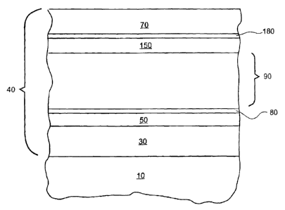
In certain preferred embodiments, the low-emissivity coating 40 comprises
a concentration-modulated middle coat 90. Here, the coating 40 includes two
infrared-reflective layers 50, 150 (e.g., comprising silver) between which is
positioned the concentration-modulated middle coat 90. Certain embodiments of
this nature are exemplified in Figure 1, wherein the illustrated coating 40
comprises, in sequence outwardly (i.e., in sequence moving away from the
substrate): a dielectric inner coat 30; a first infrared-reflective layer 50;
an optional
first blocker layer 80; the concentration-modulated middle coat 90; a second
infrared-reflective layer 150; an optional second blocker layer 180; and a
dielectric
outer coat 70. In these embodiments, the inner and outer coats can be formed
of
any desired dielectric films, including conventional homogenous dielectric
layers
(i.e., non-graded layers). Alternatively, one or both of the inner and outer
coats
can also have a graded composition, as described below.
CA 02530443 2005-12-22
WO 2005/003049 PCT/US2004/020128
13
The concentration-modulated middle coat 90 can be provided in various
forms. Preferably, this middle coat 90 includes at least one graded film
region. In
other words, at least a portion of the concentration-modulated middle coat
preferably has a graded composition (e.g., a composition that changes
gradually
with increasing distance from the substrate). By providing the middle coat 90
with
one or more graded film regions, the coating 40 can be designed to achieve an
exceptional range of color and antireflection properties. Further, special
optical
effects can be achieved using graded film. Moreover, the graded composition of
the concentration-modulated middle coat is desirable in terms of low stress
and
good adhesion properties. For example, it eliminates discrete interfaces that
would otherwise be candidates for delamination. In certain preferred
embodiments, the middle coat 90 does not include any (i.e., is entirely free
of)
discrete interfaces between dielectric layers (e.g., between homogenous
dielectric
layers). For example, the entire middle coat 90 can be designed to have a
gradually changing composition, with smooth transition from one dielectric
material to the next.
In more detail, the concentration-modulated middle coat 90 includes a first
graded film region having a substantially (or at least generally) continuously
decreasing concentration of a first dielectric material and a substantially
(or at
least generally) continuously increasing concentration of a second dielectric
material. Here, the first and second dielectric materials are different
materials.
Thus, the graded film region transitions (with increasing distance from the
substrate) from one dielectric material to another dielectric material.
Preferably,
the concentration of the first dielectric material decreases gradually as the
concentration of the second dielectric material increases gradually. Thus,
there is
preferably a smooth transition from one dielectric material to another. A
middle
coat 90 of this nature is superior (in terms of stress, adhesion, and color
and
antireflection opportunity) to a conventional middle coat formed by a
plurality of
discrete homogenous layers.
Thus, the middle coat 90 desirably includes a graded film region having a
composition that transitions (as a function of film thickness) from one
dielectric
material to another. A wide variety of dielectric materials can be used in the
CA 02530443 2005-12-22
WO 2005/003049 PCT/US2004/020128
14
graded film region. The term "dielectric" is used herein to refer to any non-
metallic
(i.e., neither a pure metal nor a metal alloy) compound that includes any one
or
more metals. In certain embodiments, each dielectric is a transparent
dielectric
that is generally or substantially transparent when deposited as a thin film.
Included in the "dielectric" definition would be any metal oxide, metal
nitride, metal
carbide, metal sulfide, metal boride, and any combination thereof (e.g., an
oxynitride). Further, the term "metal" is to be understood to include all
metals and
semi-metals (i.e., metalloids). Useful metal oxides include oxides of zinc,
tin,
indium, bismuth, titanium, hafnium, zirconium, and mixtures thereof. While
metal
oxides are desirable due to their ease and low cost of application, known
metal
nitrides (e.g., silicon nitride) can also be used. Skilled artisans will be
familiar with
other useful materials.
With respect to the graded nature of the film, in preferred embodiments the
film in each graded film region is graded in a common manner over the entire
area
of the coated surface. Thus, at any given "x, y" location on the coated
surface
(where x and y are dimensions along two respective perpendicular axes on the
coated surface), there exists the graded film (i.e., the described transition
from
one dielectric to another). The "z" dimension (i.e., the film thickness
dimension)
range over which the graded film region exists may vary slightly from one x, y
location to another, e.g., due to local variations in the surface roughness of
the
substrate. For example, this could result by sputtering the coating over a
glass
substrate having preexisting surface roughness.
Preferably, the refractive index is substantially constant over the graded
film region. That is, the graded film region preferably transitions from one
dielectric material having a given refractive index to another dielectric
material
having substantially the same refractive index. Generally, this refractive
index is
between about 1.9 and about 2.75, preferably between about 1.9 and about 2.4,
more preferably between about 1.9 and about 2.2, and perhaps optimally about
2Ø In alternate embodiments, the refractive index of the film in the graded
film
region varies, but not outside the range of 1.9-2.75, preferably not outside
the
range of 1.9-2.4, and perhaps optimally not outside the range of 1.9-2.2.
CA 02530443 2005-12-22
WO 2005/003049 PCT/US2004/020128
In certain particularly preferred embodiments, the refractive index is
substantially constant over the entire thickness of the concentration-
modulated
middle coat 90. Here, even though the composition of the middle coat 90
changes with increasing distance from the substrate (at least across a portion
of
5 the middle coat 90), the refractive index is substantially uniform across an
entire
thickness of the middle coat 90. This refractive index is generally between
about
1.9 and about 2.75, preferably between about 1.9 and about 2.4, more
preferably
between about 1.9 and about 2.2, and perhaps optimally about 2Ø In alternate
embodiments, the refractive index of the film in the middle coat 90 varies,
but not
10 outside the range of 1.9-2.75, preferably not outside the range of 1.9-2.4,
and
perhaps optimally not outside the range of 1.9-2.2.
In certain favored embodiments, the concentration-modulated middle coat
90 is formed entirely of oxide film, or of nitride film, etc. For example, the
middle
coat 90 can be deposited using a single reactive gas type (oxidizing,
nitriding,
15 etc.) It will be appreciated that impurity gases may also be present in
small
amounts during deposition, such that the middle coat may include trace
impurities.
Particularly favored are methods wherein the middle coat includes at least one
graded film region and is deposited using only oxidizing atmosphere, such that
the
middle coat is formed entirely of oxide film. Preferably, the middle coat
includes at
least one film region comprising tin oxide or zinc tin oxide, both of which
are
particularly desirable due to, inter alia, their morphology.
In certain embodiments, the first and second dielectric materials are two
different oxides selected from the group consisting of zinc oxide, tin oxide,
zinc tin
oxide (e.g., Zn2SnO4), zinc aluminum oxide (e.g., ZnOAI2O3), and titanium
oxide.
Preferably, at least one of the first and second dielectric materials is tin
oxide or
zinc tin oxide. For example, the first and second dielectric materials can be
two
different oxides selected from the group consisting of zinc oxide, tin oxide,
and
zinc tin oxide. It is to be understood, however, that in other embodiments any
two
dielectric materials can be used. For example, the first and second dielectric
materials can be selected and varied to meet the requirements of many
different
applications.
CA 02530443 2005-12-22
WO 2005/003049 PCT/US2004/020128
16
Thus, the concentration-modulated middle coat includes at least one
graded film region characterized by a transition from one dielectric material
to
another. In some cases, this middle coat includes only one graded film region.
In
such cases, the second dielectric is preferably zinc oxide, while the first
dielectric
is preferably an oxide selected from the group consisting of tin oxide, zinc
tin
oxide, and titanium oxide, perhaps optimally tin oxide or zinc tin oxide. In
one
embodiment, the first dielectric is tin oxide, and the first graded film
region extends
from a tin oxide-rich inner area (adjacent the first infrared-reflective layer
50, e.g.,
over blocker layer 80 if provided) to a zinc oxide-rich outer area (adjacent
the
second infrared-reflective layer 150). Here, the tin oxide-rich inner area is
preferably deposited directly over a first blocker layer 80, and the second
infrared-
reflective layer 150 is preferably deposited directly over the zinc oxide-rich
outer
area. This zinc oxide-rich outer area desirably comprises at least about 40A
of
essentially pure zinc oxide directly beneath the second infrared-reflective
layer
150, at least if this layer 150 comprises silver.
Thus, the middle coat 90 may comprise a single graded film region
extending from a tin oxide-rich inner area to a zinc oxide-rich outer area. In
such
embodiments, the middle coat includes at least two high concentration areas
(the
tin oxide-rich inner area is a first high concentration area and the zinc
oxide-rich
outer area is a second high concentration area). Each high concentration area
is
a thickness of film having a local maximum concentration of a desired
dielectric
material. In some cases, each high concentration area has a major
concentration
(i.e., 50% or more) of the desired dielectric material. If so desired, each
high
concentration area can be a thickness of film consisting essentially of the
desired
dielectric material. For example, each high concentration area can comprise a
homogenous film region consisting essentially of the desired dielectric
material.
Table I depicts an embodiment wherein the middle coat 90 comprises, in a
contiguous sequence moving outwardly: (1) a first homogenous film region
consisting essentially of tin oxide; (2) a first graded film region having a
substantially continuously decreasing concentration of tin oxide and a
substantially continuously increasing concentration of zinc oxide; and (3) a
second
homogenous film region consisting essentially of zinc oxide. Here, the second
CA 02530443 2005-12-22
WO 2005/003049 PCT/US2004/020128
17
homogenous film region desirably comprises at least about 40A of essentially
pure zinc oxide directly beneath the second infrared-reflective layer 150,
which
desirably is a silver film (but may simply include some silver or be an
infrared-
reflective film that does not contain silver, as may also be the case in any
of the
tables of the present disclosure).
The symbol "-p" (i.e., an arrow) is used herein to refer to a change (e.g., a
gradual change) in film composition, with increasing distance from the
substrate,
from the dielectric material identified at the base of the arrow to the
dielectric
material identified at the tip of the arrow.
Table I
glass/inner coat/silver/blocker/tin oxide-zinc oxide/silver/blocker/outer coat
Thus, in certain embodiments, the middle coat includes at least one
homogenous film region. The film in each homogenous film region does not have
a composition that is graded or otherwise varied as a function of film
thickness/distance from the substrate. Rather, each such region is a thickness
of
film having a homogenous composition (of a desired dielectric material).
Preferably, each homogenous film region is bounded by (and transitions
gradually
into) one or two graded film regions. In contrast, a conventional discrete
homogenous dielectric layer is bounded by two discrete interfaces with other
layers. In some cases, the middle coat 90 includes a plurality of homogenous
film
regions, each formed of a desired dielectric material. In these cases, each
homogenous film region preferably has a thickness of less than 200A, and
perhaps more preferably less than about 180A, and perhaps optimally less than
about 175A. These thickness limits are desirable for minimizing stress,
maximizing adhesion, limiting defect growth, and avoiding haze formation,
e.g.,
during heat treatment. Thus, in some embodiments, the middle coat 90 does not
include any homogenous film region having a thickness of 200A or more.
CA 02530443 2005-12-22
WO 2005/003049 PCT/US2004/020128
18
Notwithstanding the foregoing, it is to be appreciated that the middle coat
90 need not include any homogenous film region(s). For example, the invention
provides embodiments wherein the concentration of the entire middle coat 90
changes constantly with increasing distance from the substrate. In many
embodiments, though, the middle coat comprises at least one homogenous film
region (e.g., at least about 40 angstroms of essentially pure zinc oxide
directly
beneath the second infrared-reflective layer 150).
The invention provides several particularly desirable middle coat designs.
A first design provides a middle coat 90 comprising two graded film regions
interposed among three high concentration areas. Embodiments of this nature
are exemplified in Figure 2. A second design provides a middle coat 90
comprising three graded film regions interposed among five high concentration
areas. Embodiments of this nature are exemplified in Figure 3. In Figures 2
and
3, each high concentration area is identified by the reference character 90'
and
each row of arrows identifies a graded film region. Each of these two designs
yields an exceptional "double-type" low-emissivity coating (i.e., a coating
having
two infrared-reflective layers). For example, these designs have a symmetrical
configuration that yields exceptional optical properties.
In the first design, the concentration-modulated middle coat 90 includes
three high concentration areas and two graded film regions. For example, the
middle coat 90 can comprise, in a contiguous sequence moving outwardly: a
first
high concentration area; a first graded film region; a second high
concentration
area; a second graded film region; and a third high concentration area. Here,
the
first high concentration area is rich in a first dielectric material, the
second high
concentration area is rich in a second dielectric material, and the third high
concentration area is rich in a third dielectric material. The first graded
film region
has a substantially continuously decreasing concentration of the first
dielectric and
a substantially continuously increasing concentration of the second
dielectric. The
second graded film region has a substantially continuously decreasing
concentration of the second dielectric and a substantially continuously
increasing
concentration of the third dielectric. In these embodiments, the first and
second
dielectrics are different materials, and the second and third dielectrics are
different
CA 02530443 2005-12-22
WO 2005/003049 PCT/US2004/020128
19
materials, however the first and third dielectrics can be the same material.
Preferably, at least one of the first, second, and third dielectric materials
is tin
oxide or zinc tin oxide.
In preferred embodiments of this nature, the third dielectric material is zinc
oxide, such that the third high concentration area is a zinc oxide-rich area.
Table
2 exemplifies such coatings. Preferably, the second infrared-reflective layer
150
comprises silver positioned directly over the zinc oxide-rich, third high
concentration area, which desirably comprises at least about 40A of
essentially
pure zinc oxide.
In the embodiments of Figure 2, the first and third dielectrics can both be
the same material, such that the first and third high concentration areas are
both
rich in the same material. In preferred embodiments of this nature, the first
and
third dielectrics are both zinc oxide such that the first and third high
concentration
areas are both zinc oxide-rich areas. In these embodiments, the second
dielectric
material desirably is an oxide selected from the group consisting of tin
oxide, zinc
tin oxide, zinc aluminum oxide, and titanium oxide, preferably tin oxide or
zinc tin
oxide.
In some cases, the first, second, and third high concentration areas 90' all
comprise homogenous film regions. That is, the first high concentration area
comprises a first homogenous film region consisting essentially of a first
dielectric
material, the second high concentration area comprises a second homogenous
film region consisting essentially of a second dielectric material, and the
third high
concentration area comprises a third homogenous film region consisting
essentially of a third dielectric material. In these embodiments, each
homogenous
film region desirably has a thickness of less than 200A. Conjointly, the
second
homogenous film region desirably has a thickness of less than about 180A.
Table 2
glass/inner coat/silver/blocker/zinc oxide-tin oxide-zinc
oxide/silver/blocker/outer coat
glass/inner coat/silver/blocker/zinc oxide-zinc tin oxide-zinc
oxide/silver/blocker/outer coat
CA 02530443 2005-12-22
WO 2005/003049 PCT/US2004/020128
glass/inner coat/silver/blocker/zinc oxide-zinc aluminum oxide-zinc
oxide/silver/blocker/outer coat
glass/inner coat/silver/blocker/zinc oxide-titanium oxide-zinc
oxide/silver/blocker/outer coat
glass/inner coat/silver/blocker/zinc tin oxide-tin oxide-zinc
oxide/silver/blocker/outer coat
glass/inner coat/silver/blocker/zinc tin oxide-zinc aluminum oxide-zinc
oxide/silver/blocker/outer
5 coat
glass/inner coat/silver/blocker/zinc tin oxide-titanium oxide-zinc
oxide/silver/blocker/outer coat
glass/inner coat/silver/blocker/zinc aluminum oxide-tin oxide-zinc
oxide/silver/blocker/outer coat
glass/inner coat/silver/blocker/zinc aluminum oxide-zinc tin oxide-zinc
oxide/silver/blocker/outer
coat
10 glass/inner coat/silver/blocker/zinc aluminum oxide-titanium oxide-zinc
oxide/silver/blocker/outer
coat
In the embodiments of Figure 3, the concentration-modulated middle coat
15 90 includes five high concentration areas and four graded film regions.
Here, the
middle coat 90 comprises, in a contiguous sequence moving outwardly: a first
high concentration area; a first graded film region; a second high
concentration
area; a second graded film region; a third high concentration area; a third
graded
film region; a fourth high concentration area; a fourth graded film region;
and a
20 fifth high concentration area. In more detail, the first high concentration
area is
rich in a first dielectric material, the second high concentration area is
rich in a
second dielectric material, the third high concentration area is rich in a
third
dielectric material, the fourth high concentration area is rich in a fourth
dielectric
material, and the fifth high concentration area is rich in a fifth dielectric
material.
The first graded film region has a substantially continuously decreasing
concentration of the first dielectric and a substantially continuously
increasing
concentration of the second dielectric. The second graded film region has a
substantially continuously decreasing concentration of the second dielectric
and a
substantially continuously increasing concentration of the third dielectric.
The
third graded film region has a substantially continuously decreasing
concentration
of the third dielectric and a substantially continuously increasing
concentration of
CA 02530443 2005-12-22
WO 2005/003049 PCT/US2004/020128
21
the fourth dielectric. The fourth graded film region has a substantially
continuously decreasing concentration of the fourth dielectric and a
substantially
continuously increasing concentration of the fifth dielectric. In these
embodiments, the first and second dielectrics are different materials, the
second
and third dielectrics are different materials, the third and fourth
dielectrics are
different materials, and the fourth and fifth dielectrics are different
materials.
However, the first and fifth dielectrics can be the same material, the second
and
fourth dielectrics can be the same material, etc. Preferably, at least one of
the
first, second, third, fourth, and fifth dielectric materials is tin oxide or
zinc tin oxide.
In preferred embodiments of this nature, the fifth dielectric material is zinc
oxide, such that the fifth high concentration area is a zinc oxide-rich area.
Table 3
exemplifies coatings of this nature. Preferably, the second infrared-
reflective layer
150 comprises silver positioned directly over the zinc oxide-rich, fifth high
concentration area, which desirably comprises at least about 40A of
essentially
pure zinc oxide.
In the embodiments of Figure 3, the first, third, and fifth dielectrics can
all
be the same material, such that the first, third, and fifth high concentration
areas
are all rich in the same material. In preferred embodiments of this nature,
the first,
third, and fifth dielectrics are all zinc oxide (i.e., the first, third, and
fifth high
concentration areas are all zinc oxide-rich areas). Alternatively or
additionally, the
second and fourth dielectrics can both be the same material, such that the
second
and fourth high concentration areas are both rich in the same material. For
example, the second and fourth dielectric materials can both be an oxide
selected
from the group consisting of tin oxide, zinc tin oxide, zinc aluminum oxide,
and
titanium oxide, perhaps optimally tin oxide or zinc tin oxide.
Table 3
glass/inner coat/silver/blocker/zinc oxide-tin oxide-zinc oxide-tin oxide-zinc
oxide/silver/blocker/outer coat
CA 02530443 2005-12-22
WO 2005/003049 PCT/US2004/020128
22
glass/inner coat/silver/blocker/zinc oxide-zinc tin oxide-zinc oxide-zinc tin
oxide-zinc
oxide/silver/blocker/outer coat
glass/inner coat/silver/blocker/zinc oxide-zinc aluminum oxide-zinc oxide-zinc
aluminum
oxide-zinc oxide/silver/blocker/outer coat
glass/inner coat/silver/blocker/zinc oxide-titanium oxide-zinc oxide-titanium
oxide-zinc
oxide/silver/blocker/outer coat
glass/inner coat/silver/blocker/zinc tin oxide-tin oxide-zinc tin oxide-tin
oxide-zinc
oxide/silver/blocker/outer coat
glass/inner coat/silver/blocker/zinc tin oxide-zinc aluminum oxide-zinc tin
oxide-zinc
aluminum oxide-zinc oxide/silver/blocker/outer coat
glass/inner coat/silver/blocker/zinc tin oxide-titanium oxide-zinc tin oxide-
titanium
oxide-zinc oxide/silver/blocker/outer coat
glass/inner coat/silver/blocker/zinc aluminum oxide-tin oxide-zinc aluminum
oxide-tin
oxide-zinc oxide/silver/blocker/outer coat
glass/inner coat/silver/blocker/zinc aluminum oxide-zinc tin oxide-zinc
aluminum
oxide-zinc tin oxide-zinc oxide/silver/blocker/outer coat
glass/inner coat/silver/blocker/zinc aluminum oxide-titanium oxide-zinc
aluminum
oxide-titanium oxide-zinc oxide/silver/blocker/outer coat
glass/inner coat/silver/blocker/tin oxide-zinc tin oxide-tin oxide-zinc tin
oxide-zinc
oxide/silver/blocker/outer coat
glass/inner coat/silver/blocker/tin oxide-zinc aluminum oxide-tin oxide-zinc
aluminum
oxide-zinc oxide/silver/blocker/outer coat
glass/inner coat/silver/blocker/tin oxide-titanium oxide-tin oxide-titanium
oxide-zinc
oxide/silver/blocker/outer coat
In certain embodiments, the first, second, third, fourth, and fifth high
concentration areas all comprise homogenous film regions. That is, the first
high
concentration area comprises a first homogenous film region consisting
essentially of a first dielectric material, the second high concentration area
CA 02530443 2005-12-22
WO 2005/003049 PCT/US2004/020128
23
comprises a second homogenous film region consisting essentially of a second
dielectric material, the third high concentration area comprises a third
homogenous film region consisting essentially of a third dielectric material,
the
fourth high concentration area comprises a fourth homogenous film region
consisting essentially of a fourth dielectric material, and the fifth high
concentration area comprises a fifth homogenous film region consisting
essentially of a fifth dielectric material. In these embodiments, each
homogenous
film region desirably has a thickness of less than 200A. Conjointly, the
second
and fourth homogenous film regions each desirably has a thickness of less than
about 180A.
In one embodiment, the first dielectric material is zinc oxide, the second
dielectric material is tin oxide, the third dielectric material is titanium
oxide (or zinc
tin oxide), the fourth dielectric material is tin oxide, and the fifth
dielectric material
is zinc oxide. In another embodiment, the first dielectric material is zinc
oxide, the
second dielectric material is titanium oxide, the third dielectric material is
tin oxide
(or zinc tin oxide), the fourth dielectric material is titanium oxide, and the
fifth
dielectric material is zinc oxide. In still another embodiment, the first
dielectric
material is zinc oxide, the second dielectric material is zinc tin oxide, the
third
dielectric material is tin oxide (or titanium oxide), the fourth dielectric
material is
zinc tin oxide, and the fifth dielectric material is zinc oxide. In yet
another
embodiment, the first dielectric material is zinc tin oxide, the second
dielectric
material is tin oxide, the third dielectric material is titanium oxide, the
fourth
dielectric material is tin oxide, and the fifth dielectric material is zinc
oxide. In still
another embodiment, the first dielectric material is zinc tin oxide, the
second
dielectric material is titanium oxide, the third dielectric material is tin
oxide, the
fourth dielectric material is titanium oxide, and the fifth dielectric
material is zinc
oxide. In yet another embodiment, the first dielectric material is tin oxide,
the
second dielectric material is titanium oxide, the third dielectric material is
zinc tin
oxide, the fourth dielectric material is titanium oxide, and the fifth
dielectric
material is zinc oxide. In a further embodiment, the first dielectric material
is tin
oxide, the second dielectric material is zinc tin oxide, the third dielectric
material is
CA 02530443 2005-12-22
WO 2005/003049 PCT/US2004/020128
24
titanium oxide, the fourth dielectric material is tin oxide, and the fifth
dielectric
material is zinc oxide. Many other variations will be apparent to skilled
artisans.
It is particularly preferred to provide the coating 40 with a concentration-
modulated middle coat 90. The middle coat of a double-type low-emissivity
coating characteristically has a relatively great thickness. For example, it
is
common for the middle coat to be at least about twice as thick as the inner
coat
and/or at least about twice as thick as the outer coat. As a result, the
drawbacks
associated with thick dielectric layers are particularly acute with respect to
the
middle coat. It is thus particularly preferred, especially in terms of reduced
stress,
to provide the middle coat with the graded film region(s) described above.
Various embodiments have been described wherein the coating 40 has a
concentration-modulated middle coat 90. In some of these embodiments, the
coating is also provided with a concentration-modulated inner coat 30. Here,
the
inner coat includes a graded film region having a substantially continuously
decreasing concentration of one desired dielectric and a substantially
continuously
increasing concentration of another desired dielectric. In embodiments of this
nature, the coating can also be provided with a concentration-modulated outer
coat. Here, the outer coat includes a third graded film region having a
substantially continuously decreasing concentration of one dielectric and a
substantially continuously increasing concentration of another dielectric. In
these
embodiments, the concentration-modulated inner, middle, and outer coats
preferably do not include any discrete interfaces between homogenous
dielectric
layers.
Thus, the invention provides desirable embodiments wherein the coating
40 includes a concentration-modulated inner coat 30, a concentration-modulated
middle coat 90, and a concentration-modulated outer coat 70. Table 4
exemplifies
coatings of this nature. Here, the terms "D1 ", "D2", etc. refer respectively
to a first
dielectric material, a second dielectric material, etc. (D1 and D2 are
different
materials, and so on, though, D1 and D3 can be the same material, etc.). As
noted above, each arrow represents a film composition gradient wherein, with
increasing distance from the substrate, the composition of the film
transitions from
one material (the material identified left of the arrow) to another material
(the
CA 02530443 2005-12-22
WO 2005/003049 PCT/US2004/020128
material identified right of the arrow). These embodiments do not require use
of
any particular dielectric materials. Rather, any desired dielectrics can be
used.
Certain dielectrics, however, are preferred. Preferably, all the film in the
base coat
is deposited using the same reactive gas type (oxidizing, or nitriding, etc.),
5 such that the base coat consists essentially of oxide film or nitride film,
etc. This is
also preferable for the middle 90 and outer 70 coats, as it allows for
particularly
convenient deposition methods. In particularly preferred embodiments, the
entire
coating 40 does not (or at least the inner coat 30, the middle coat 90, and
the
outer coat 70 do not) include any discrete interfaces between homogenous
10 dielectric layers.
Table 4
15 glass/D1- >D2/silver/blocker/D3-->D4/silver/blocker/D5-->D6
glass/D1 -).D2/silver/blocker/D3->D4-+D5/silver/blocker/D6--D7
glass/D1 -->D2/silver/blocker/D3--+D4->D5-->D6->D7/silver/blocker/D8-->D9
glass/D1 -D2-->D3/silver/blocker/D4->D5-->D6/silver/blocker/D7->D8
glass/D1- >D2/silver/blocker/D3-+D4-->D5/silver/blocker/D6->D7-*D8
The invention provides a number of embodiments wherein the coating
comprises a particularly desirable concentration-modulated inner coat. Here,
the
modulated inner coat has an inner area comprising tin oxide and an outer area
comprising zinc oxide, zinc tin oxide, or zinc aluminum oxide. In some
embodiments of this nature, the coating 40 is a double-type low-emissivity
coating
comprising, in sequence outwardly: a concentration-modulated inner coat 30; a
first infrared-reflective layer 50; an optional first blocker layer 80; a
dielectric
middle coat 90; a second infrared-reflective layer 150; an optional second
blocker
layer 180; and a dielectric outer coat 70. Here, the middle and outer coats
can be
formed of any desired dielectric films, including conventional homogenous
CA 02530443 2005-12-22
WO 2005/003049 PCT/US2004/020128
26
dielectric layers. Alternatively, one or both of the middle and outer coats
can have
a graded composition, as noted above. In other embodiments of this nature, the
coating is a "single type" low-emissivity coating (i.e., a low-emissivity
coating
having a single infrared-reflective layer) comprising, in sequence outwardly:
a
concentration-modulated inner coat; an infrared-reflective layer; an optional
blocker layer; and a dielectric outer coat. Here, the outer coat can be formed
of
any desired dielectric films, including conventional homogenous dielectric
layers.
Alternatively, the outer coat can have a graded composition.
Preferably, the concentration-modulated inner coat includes a first graded
film region having a substantially continuously decreasing concentration of
tin
oxide and a substantially continuously increasing concentration of zinc oxide,
zinc
tin oxide, or zinc aluminum oxide. Table 5 exemplifies coatings of this
nature.
Here, the first graded film region has an inner area that is rich in tin oxide
and an
outer area that is rich in zinc oxide, zinc tin oxide, or zinc aluminum oxide.
Perhaps optimally, the outer area is rich in zinc oxide. An inner coat of this
nature
can be produced, for example, using the sputtering apparatus depicted in
Figure
5B. In embodiments of this nature, the infrared-reflective layer 50 is
desirably
deposited directly over the zinc oxide-rich outer area of the inner coat.
Conjointly,
this zinc oxide-rich outer area desirably comprises at least about 40
angstroms of
essentially pure zinc oxide, while the infrared-reflective layer 50 desirably
is a
silver film.
Table 5
glass/tin oxide-zinc oxide/silver/blocker/middle coat/silver/blocker/outer
coat
glass/tin oxide-zinc oxide/silver/blocker/outer coat
glass/tin oxide-zinc tin oxide/silver/blocker/middle coat/silver/blocker/outer
coat
glass/tin oxide-zinc tin oxide/silver/blocker/outer coat
glass/tin oxide-zinc aluminum oxide/silver/blocker/middle
coat/silver/blocker/outer coat
glass/tin oxide-zinc aluminum oxide/silver/blocker/outer coat
CA 02530443 2005-12-22
WO 2005/003049 PCT/US2004/020128
27
In the embodiments of Table 5, the tin oxide-rich inner area (which
preferably consists essentially of tin oxide) can be deposited directly over
the
substrate. Alternatively, the coating can further include a transparent base
layer
comprising silicon dioxide deposited directly over the substrate (preferably
at less
than 100A, and perhaps optimally at about 50A-100A). In such cases, the tin
oxide-rich inner area is preferably deposited directly over the silicon
dioxide.
Some preferred embodiments of this nature are exemplified by the first six
coatings in Table 6. Other preferred embodiments are exemplified by the last
six
coatings in Table 6, wherein the silicon dioxide is deposited directly over
the
substrate, and this silicon dioxide transitions to tin oxide, which
subsequently
transitions to zinc oxide, zinc tin oxide, or zinc aluminum oxide. These
embodiments provide an extraordinarily durable foundation for the coating.
Table 6
glass/silicon dioxide/tin oxide-zinc oxide/silver/blocker/middle
coat/silver/blocker/outer coat
glass/silicon dioxide/tin oxide-zinc tin oxide/silver/blocker/middle
coat/silver/blocker/outer coat
glass/silicon dioxide/tin oxide-zinc aluminum oxide/silver/blocker/middle
coat/silver/blocker/outer
coat
glass/silicon dioxide/tin, oxide-zinc oxide/silver/blocker/outer coat
glass/silicon dioxide/tin oxide-zinc tin oxide/silver/blocker/outer coat
glass/silicon dioxide/tin oxide-zinc aluminum oxide/silver/blocker/outer coat
glass/silicon dioxide-tin oxide-zinc oxide/silver/blocker/middle
coat/silver/blocker/outer coat
glass/silicon dioxide-tin oxide-zinc tin oxide/silver/blocker/middle
coat/silver/blocker/outer coat
glass/silicon dioxide-tin oxide-zinc aluminum oxide/silver/blocker/middle
coat/silver/blocker/outer
coat
glass/silicon dioxide-tin oxide-zinc oxide/silver/blocker/outer coat
glass/silicon dioxide-tin oxide-zinc tin oxide/silver/blocker/outer coat
glass/silicon dioxide-tin oxide-zinc aluminum oxide/silver/blocker/outer coat
CA 02530443 2005-12-22
WO 2005/003049 PCT/US2004/020128
28
In certain preferred embodiments, the invention provides a concentration-
modulated inner coat comprising in a contiguous sequence moving outwardly: (i)
a
first high concentration area, the first high concentration area being rich in
tin
oxide; (ii) a first graded film region having a substantially continuously
decreasing
concentration of tin oxide and a substantially continuously increasing
concentration of zinc oxide; (iii) a second high concentration area, the
second high
concentration area being rich in zinc oxide; (iv) a second graded film region
having a substantially continuously decreasing concentration of zinc oxide and
a
substantially continuously increasing concentration of tin oxide; (v) a third
high
concentration area, the third high concentration area being rich in tin oxide;
(vi) a
third graded film region having a substantially continuously decreasing
concentration of tin oxide and a substantially continuously increasing
concentration of zinc oxide; and (vii) a fourth high concentration area, the
fourth
high concentration area being rich in zinc oxide. An inner coat of this nature
can
be produced, for example, using the sputtering apparatus of Figure 5A.
With respect to the infrared-reflective film, silver preferably is used. While
other infrared-reflective metals (e.g., copper, gold, platinum, palladium,
nickel, and
alloys) can be used, silver provides the lowest emissivity and best color
neutrality.
In other cases, the infrared-reflective film comprises material other than
silver, but
is entirely metallic or essentially metallic (comprising no more than one
atomic
percent of non-metal material). Preferably, though, pure silver or
substantially
pure silver (comprising no more than five atomic percent of other material) is
used. This provides the lowest emissivity possible. Each infrared-reflective
film
can, for example, be deposited by sputtering a silver target in an inert
atmosphere. Each infrared-reflective film may have discrete inner and outer
interfaces with the underlying and overlying films, respectively. In a double-
type
low-emissivity coating, for example, a first silver film may have a discrete
inner
interface with an underlying inner coat 30 and a discrete outer interface with
an
overlying film (which may be a blocker layer 80 or the middle coat 90), and a
second silver film may have a discrete inner interface with an underlying
middle
CA 02530443 2005-12-22
WO 2005/003049 PCT/US2004/020128
29
coat 90 and a discrete outer interface with an overlying film (which may be a
blocker layer 180 or the outer coat 70). These embodiments are preferred
because, inter alia, they impart exceptionally low emissivity in the coating
40.
Preferably, the total physical thickness of the inner coat is less than 200
angstroms. Each infrared-reflective (e.g., silver) film preferably has a
physical
thickness of between about 40 angstroms and about 190 angstroms. In
embodiments wherein the coating includes two infrared-reflective films, the
middle
coat desirably has a total physical thickness of between about 150 angstroms
and
about 700 angstroms. The total physical thickness of the outer coat, whether
the
coating has one or more infrared-reflective layers, is preferably between
about
100 angstroms and about 300 angstroms. It is to be understood, however, that
the thickness ranges noted in this paragraph are merely preferred, and many
embodiments are anticipated wherein the actual thicknesses will fall outside
these
ranges.
In certain embodiments, the coating includes one or more graded film
region each transitioning from a first oxide of zinc and tin to a second oxide
of zinc
and tin. For example, such a graded film region may be formed by sequentially
conveying a substrate past the following sputtering targets: a first target
formed of
pure or essentially pure tin, a second target formed of a high tin content
(e.g.,
about 40% tin or more) zinc-tin material, a third target formed of a low tin
content
(e.g., about 20% tin or less) zinc-tin material, and a fourth target formed of
pure or
essentially pure zinc. A graded film region of this nature can be used in the
inner
coat, the middle coat, or the outer coat.
The invention also provides desirable methods for producing coated
substrates. Generally, these methods involve depositing a coating 40 that
includes a dielectric inner coat 30, a dielectric middle coat 90, and a
dielectric
outer coat 70, at least one of which comprises a graded film region. Various
suitable coatings of this nature have been described, and the present methods
extend to the deposition of any of the described coatings.
The present methods preferably involve depositing graded film without
producing any abrupt change in film composition (such that the composition of
the
film in each graded film region has no sudden discontinuity). Preferably, the
CA 02530443 2005-12-22
WO 2005/003049 PCT/US2004/020128
graded film is deposited so as to provide a gradual transition from one
dielectric
material to the next (as a function of film thickness/distance from the
substrate).
This is desirably accomplished by a sputtering process that involves using a
common target material for the last target in a desired sputtering bay and for
the
5 first (or only) target in the subsequent bay, and by using a common target
material
for the first target in the desired bay and for the last (or only) target in
the
preceding bay. In certain embodiments, each sputtering bay is separated from
each adjacent bay by at least one chamber wall. This wall characteristically
defines a narrow passage through which substrates can be conveyed (e.g., over
10 rollers or other substrate supports defining a path of substrate travel)
from one
bay to the next. The present methods allow manufacturers to optimize the
properties of the dielectric inner, middle, and/or outer coats, while avoiding
discrete interfaces, where stress tends otherwise to pile up (i.e., be
concentrated)..
In certain embodiments, the method comprises conveying a substrate
15 through at least three adjacent sputtering bays each adapted for depositing
dielectric film (e.g., each containing a reactive sputtering atmosphere and/or
a
ceramic target). The term "adjacent sputtering bays" is used herein to refer
to
sputtering bays through which a substrate is conveyed sequentially without
being
passed through any other bay. At least one of these three bays is equipped
with
20 two or more sputtering targets, of which at least two carry different
sputterable
materials. The first target in this bay (the "transition" bay) carries the
same
sputterable material as the last (or only) target in the preceding bay. The
last
target in the transition bay carries the same sputterable material as the
first (or
only) target in the subsequent bay. This is perhaps best understood with
25 reference to Figures 4-5B. (It is to be understood that the targets in the
transition
bay are sputtered in a common (i.e., shared) sputtering atmosphere.)
Figure 4 depicts one particular sputtering apparatus that can be used to
deposit a concentration-modulated middle coat 90. This arrangement of
sputtering targets can be used, for example, to produce the middle coat of the
first
30 coating in Table 3. Here, the substrate is conveyed through two sputtering
bays
each equipped with two zinc targets. These two bays are preferably provided
with
an oxidizing atmosphere, as is preferred in all the bays. The innermost area
of
CA 02530443 2005-12-22
WO 2005/003049 PCT/US2004/020128
31
the middle coat is thus deposited as a first homogenous film region, which
consists essentially of zinc oxide. Next, the substrate is conveyed through a
bay
in which the first target is zinc and the second target is tin. As the
substrate
moves through this bay (along the path of substrate travel 99), the substrate
is
exposed initially to a relatively great amount of zinc oxide flux, and is
exposed to a
gradually decreasing amount of zinc oxide flux and a gradually increasing
amount
of tin oxide flux, and toward the end of the bay is exposed to a relatively
great
amount of tin oxide flux. Thus, a first graded film region is deposited in
this bay.
The substrate is then conveyed through a bay equipped with two tin targets. In
these two bays, there is deposited a second homogenous film region, which
consists essentially of tin oxide. Next, the substrate is conveyed through a
bay in
which the first target is tin and the second target is zinc. A second graded
film
region is deposited in this bay. The substrate is then conveyed through two
sputtering bays each equipped with two zinc targets. In these two bays, there
is
deposited a third homogenous film region, which consists essentially of zinc
oxide.
Then, the substrate is conveyed through a bay in which the first target is
zinc and
the second target is tin. Here, a third graded film region is deposited. The
substrate is then conveyed through a bay equipped with two tin targets. In
these
two bays, there is deposited a fourth homogenous film region, which consists
essentially of tin oxide. Next, the substrate is conveyed through a bay in
which'
the first target is tin and the second target is zinc. Here, a fourth graded
film
region is deposited. Finally, the substrate is conveyed through two sputtering
bays each equipped with two zinc targets, whereby the outermost area of the
middle coat is deposited as a fifth homogenous film region, which consists
essentially zinc oxide.
Thus, the substrate is not exposed to any abrupt changes in the
composition of the flux to which it is exposed when conveyed through the
sputtering line. It will be appreciated that Figure 4 only depicts part of the
sputtering line or coater through which the substrate is conveyed. The line or
coater includes other sputtering bays (not shown in Figure 4) in which the
remaining portions of the coating 40 are deposited. Sputtering lines and
coaters
CA 02530443 2005-12-22
WO 2005/003049 PCT/US2004/020128
32
are well known and therefore certain conventional details (e.g., the rollers
or other
substrate support, the bottom of the coater, etc.) are not illustrated here.
Figure 5A depicts one particular sputtering apparatus that can be used to
deposit a concentration-modulated inner coat 30. This arrangement of
sputtering
targets can be used, for example, to produce a middle coat having the
following
structure: tin oxide-*zinc oxide-tin oxide->zinc oxide. Here, the substrate is
conveyed through a sputtering bay in which the first target is tin and the
second
target is zinc. Next, the substrate is conveyed through a bay in which the
first
target is zinc and the second target is tin. The substrate is then conveyed
through
a bay in which the first target is tin and the second target is zinc. Finally,
the
substrate is conveyed through a bay in which the first target is zinc and the
second target is tin.
It is to be understood that the films stacks depicted in the tables of this
disclosure are not required to consist only of the illustrated films. Rather,
other
films can be interposed among (e.g., between, beneath, and/or over) the
illustrated films. Thus, the films in the tables are in a sequence, though not
necessarily a contiguous sequence. In preferred embodiments, though, the
illustrated films are in a contiguous sequence. Further, the tables denote
silver
infrared-reflective layers 50, 150, although it is to be understood that other
reflective materials can be used. In addition, the tabulated coatings are
denoted
as including blocker layers, although the blocker layers are not strictly
required.
For purposes of this particular disclosure, the blocker layer 80 when provided
is
not considered to be part of the middle coat 90, nor is the blocker layer 180
when
provided considered to be part of the outer coat 70. Preferably, when the
blocker
layers are provided, each blocker layer is not a homogenous dielectric layer,
but
rather has a metallic inner area and a dielectric outer area. Absent an
express
indication to the contrary, the thicknesses reported herein are physical
thicknesses, rather than optical thicknesses. The terms "substantially
continuously decreasing concentration", "substantially continuously increasing
concentration", and the like are used herein to refer to a transition, with
increasing
distance from the substrate, from one dielectric material to another, wherein
the
transition occurs over the thickness of the graded film region, rather than at
a
CA 02530443 2005-12-22
WO 2005/003049 PCT/US2004/020128
33
discrete interface where one material changes abruptly to another. Each such
transition is preferably, though not necessarily, a gradual transition. In the
disclosed embodiments involving zinc tin oxide film, the tin atoms may, for
example, account for less than about 5-10 atomic percent relative to all the
metal
atoms in the film. With respect to the aluminum in the disclosed zinc aluminum
film, the aluminum atoms may, for example, account for less than about 2
atomic
percent relative to all the metal atoms in the film.
While preferred embodiments of the present invention have been
described, it should be understood that numerous changes, adaptations, and
modifications can be made therein without departing from the spirit of the
invention and the scope of the appended claims.