Note: Descriptions are shown in the official language in which they were submitted.
CA 02530711 2005-12-23
32/15
1
DESCRIPTION
READING METHOD, RESPONDER, AND INTERROGATOR
TECHNICAL FIELD
The present invention relates to an
identification method and device for identifying
responders by transmitting and receiving a signal
between an interrogator and a plurality of responders
and in particular, to a method and a device for
performing identification by controlling congestion ef
a response signal from the interrogator and the
responders.
BACKGROUND ART
The present description references the
following documents. The documents are to be
referenced by their document numbers.
[Document 1] WO 98/21691
[Document 2] WO GO/36555
When a plurality of responders exist in an
effective radio wave area of the interrogator, it is
necessary to identify response signals from the
responders. Document 1 discloses a technique for
preventing cross talk between the responders.
The technique disclosed in Document 1 is as
follows. An interrogation signal from the interrogator
is received and the responder transmits a predetermined
CA 02530711 2005-12-23
2
number cf bits. The interrogator receives the
predetermined number of bits transmitted from the
responder and returns them to the responder. When the
number of bits returned is identical to the number of
bits transmitted, the responder transmits a
predetermined number of bits subsequent to the bits
already transmitted and repeats the same process. Pvhen
the number of bits returned is not identical to the
number of bits transmitted, the responder does not
participate in the identification process until the
next interrogation signal is received. By repeating
this process, finally, only one responder makes
identify its identification number. By repeating this
recognition process until no unprocessed responder
exists, identification of the responders is complete.
In Document 1, transmission and reception
to/from the interrogator are repeated in bit unit of a
predetermined number and accordingly, this technique
requires a logical circuit for switching between
transmission and reception and control of a memory
address counter requiring various commands
(interrogation signal, reception bit return signal,
identification failure report signal, identification
completion report signal), a plenty of operation stages
accompanying the commands, a flip-flop representing the
state transition, and a data comparison circuit.
Document 2 discloses a technique in which a
responder having a memory for storing an identification
CA 02530711 2005-12-23
3
number in accordance with the clock pulse from the
interrogator transmits the identification number. In
Document 2, the responder as RFID transmits an
identification number in accordance with the clock
pulse from the interrogator, thereby excluding a
command in communication and simplifying the
transmission/recepticn method.
DISCLOSURE OF THE INVENTION
The representative invention among the
inventions disclosed in this application can be
outlined as follows.
There are provided an interrogator reading a
recognition number in a responder by radio and the
responder. When a clock pulse is modulated to a high-
frequency carrier and transmitted to the responder from
the antenna of the interrogator, there are a first case
when the clock pulse interval is short and a second
case when the clock pulse interval is long. By
combining the clock pulse of the first case and the
clock pulse of the second case, the responder controls
reading of the identification number from the
interrogator.
BRIEF DESCRIPTION OF THE DRAWINGS
Fig. 1 is a diagram showing a clock pulse
interval discrimination circuit.
Fig. 2 is a diagram showing configuration of
CA 02530711 2005-12-23
a counter memory circuv~t according to an embodiment.
Fig. 3 is a diagram showing inside of the
responder according to the embodiment.
Fig. 4 is a diagram showing memory
configuration of the responder according to the
embodiment.
Fig. 5 is a diagram showing a counter and
memory configuration according to the embodiment.
Fig. 6 vs a diagram showing reading from the
responder according to the embodiment.
Fig. 7 is a diagram showing retry of reading
according to the embodiment.
Fig. 8 is a diagram showing a case requiring
congestion control..
Fig. 9 is a diagram showing an operation flow
of the responder according to the embodiment of the
present invention.
Fig. 10 is a diagram showing a protocol
according to the embodiment.
Fig. 11 is a diagram showing a flip-flop
according to the embodiment.
Fig. 12 is a diagram showing EB writing
according to the embodiment.
Fig. 13 is a diagram showing a memory state
according to the embodiment.
Fig. 14 is a diagram showing a clock pulse
interval detection circuit according to the embodiment.
Fig. 15 is a diagram showing internal
CA 02530711 2005-12-23
configuration of the interrogator.
Fig. 16 is a diagram showing an operation
flow of the interrogator.
BEST MODE FOR CARRYING OUT THE INVENTION
5 A large amount of RFID tags are distributed
and they become disposable since their collection cost
is large. Accord-ngly, there is a problem to reduce
the manufacturing cost of the RFID tag.
In order to arrange a plurality of RFID in
the effective radio wave area from the interrogator and
increase the effective radio area greater than the size
of the RFID mounting object and the range of the
arrangement interval, the RFID should have the
congestion co:~trol function.
in the present invention, by simplifying the
transmission/reception method in the responder and the
interrogator and simplifying the congestion control
function, the function of the RFID is minimized so that
the number of chips (RFID tags) which can be cut out
from one wafer is increased to so as to improve the
mass production. Thus, the RFID can have the
congestion control function and the manufacturing cost
per piece can be reduced.
For example, the RFID attached to a product
such as clothes requires a large collection cost and it
is commercially preferable that the RFID be disposable.
Furthermore, the congestion control is indispensable
CA 02530711 2005-12-23
6
for managing products in a box for transporting,
without opening the box. Accordingly, it is necessary
to reduce the RFID tag cost so as to enable disposing
cf the RFID tag and enable congestion control.
Fig. 8 shows an example that a plurality of
responders 902 to 906 according to the present
invention exist in the effective radio wave area 901 of
the interrogator 907. Fig. 8 shows an example of five
responders 902 to 906. Details will be give later.
Even when a plurality of responders exist in the
effective radio wave area 901, it is possible to read
out the memory of each responder by operating each
responder by the two types of clock pulses (modulation
signals), i.e., long and short clock pulses from the
interrogator.
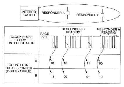
Fig. 10 shows a specific responder, a
communication method in the interrogator, and a
congestion control method. Fig. 10 shows a case when
chip A and chip B exist in the effective radio area.
Moreover, in this embodiment, each chip has 2-bit
counter for simplification. When the clock pulse from
the interrogator starts, chip A and chip B
simultaneously set the initial values of the page
numbers predetermined for the counters. In this
embodiment, the page number is Ol in chip A and 11 in
chip B. The interrogator outputs a short-interval
clock pulse to read out the memory of the responder.
However, the counter in each chip is not yet 00 and
CA 02530711 2005-12-23
each chip does not transmit the memory content. Since
no data is coming, the interrogator judges that the no
responder is operating and stops transmission of the
short-interval clock pulse and transmits a lcng-
interval clock pulse. Then, each pulse increments the
page number by +1. That is, the page number becomes 10
in chip A and 00 in chip B. Here, chip B sets an
operation switching flip-flop and transmits memory data
to the interrogator with the next short-interval clock
pulse coming, When it terminates normally, the
interrogator again transmits a long-interval clock
pulse and the counter of chip A also becomes 00 and
chip A transmits data. Like this example, chip A and
chip B can transmit memory data without being
overlapped and the interrogator rapidly turns the page
by the long-interval clock pulse, thereby reducing the
read out time of the congestion control.
Fig. 9 is a flowchart of the communication
method with the interrogator and the congestion control
method in the responder of the present invention. The
responders 902-906 demodulates a modulated signal from
the interrogator 907 and acquires the two types of
clock pulse having a long or a short interval.
As a basic operation of the responder, the
page number is counted up by the clock pulse having a
long clock interval and the memory address is counted
up by a clock pulse having a short clock interval
(hereinafter, the clock pulse having the long clock
CA 02530711 2005-12-23
8
interval will be referred to as a long clock pulse and
the clock pulse having the short clock interval will be
referred to as a short clock pulse). By employing tow
types of clock pulse having different clock intervals,
it is possible to simplify the communication method,
the congestion control method, and configuration of the
responder and the interrogator.
Moreover, in the embodiment of the present
invention, the clock interval represents a time
interval between an L level and the next L level, i.e.,
the time interval from the fall from the H level to the
L level to the next fall.
The clock width is defined by time length in
the L level state, i.e., the time interval from the
fall from the H level to the L level to the rise from
the L level to the H level. In the flowchart of Fig.
9, the clock interval and the clock width are used
separately for control.
When the operation switching flip-flop is in
the reset state, the page number is counted up and when
the operation switching flip-flop is in the set state,
the memory address is counted up.
In step 1001, the responder receives the
first clock pulse from the interrogator. The first
clock pulse may be long or short.
In step 1002, the page number (random number)
held uniquely in each responder is set as the initial
value in the counter. The page number is a number
CA 02530711 2005-12-23
O
defining the order of transmission of the
identification number when a plurality of responders
exist in the effective radio area of the interroaater.
In step 1003, the L level width of the next
clock pulse is monitcred. The responder receives the
next clock pulse and checks whether the interval is
long o_r short. When the clock pulse interval is long
(in the case of the long clock pulse), control is
passed to step 1010 and when the clock pulse interval
is short (in the case of the short clock pulse),
control is passed to step 1008.
In step 1010, the operation switching f~~ip-
flop in the responder is reset, i.e., the page number
count up is enabled, and control is passed to step
1004, where the page number set in the counter is
incremented by +1.
In step 1005, when a carry is outputted from
the counter, it is indicated that the counter content
has become zero. That is, in the binary counter, count
up is performed by one bit and after all one, the
operation is performed to all zero. When the all zero
is set, a carry is outputted. It is checked whether a
carry is outputted from the counter. When a carry is
outputted in step 1006, the operation switching flip-
flop is set by using the carry of step 1005 in the
responder. That is, count up of the memory address is
enabled. When no carry is outputted, control is
returned to step 1003 to wait for the next clock pulse.
CA 02530711 2005-12-23
l~
Step 1007 waits for the next clock pulse and
monitors the width of tie L level of the clock pulse.
When the clock pulse width is narrow, control is
returned to step 1003. When the clock pulse width is
wide, control is passed to step 1011, where a page
rmmber other than that of step 1002 is set irl the
counter, and control is returned to step 1003.
On the other hand, when control is passed
from step 1003 to step 1008, step 1008 checks whether
operation switching flip-flop in the responder is set.
When it is set, the memory address is incremented by +1
in step 1012 in Fig. 9 and control is passed to step
1009, where the number of the responder is outputted by
one bit. After tl-_is, control is passed to step 1007.
Here, it should be noted that the flow is one
of the embodiments and the branching condition of step
1003 in Fig. 9 may be vice versa and the branching
condition of step 1007 in Fig. 9 may be vice versa.
When the responder receives a clock pulse of
short interval, the responder checks whether the
operation switching flip-flop in its chip is set. When
the operation switching flip-flop is set, memory data
is outputted. Otherwise, the clock pulse of the short
interval is ignored.
Since the responder has the operation
switching flip-flop, when the flip-flop is set, the
responder transmits a number in accordance with the
clock pulse of the interrogator and when the operation
CA 02530711 2005-12-23
11
switching flip-flop is not set, the number transmission
is not performed, thereby preventing the simultaneous
operation of the responders to cause congestion of the
number transmissions.
When a plenty of radio IC tags exist at
random in the effective radio wave area, the
possibility of conflict of the page numbers becomes
high. When a plurality of responders have the same
page number, the operation switching flip-flops are set
at the same tune and the number is simultaneously
transmitted to the interrogator. Since the
interrogator receives the number from the responders by
the logical OR, the error detection code built in the
number does not become a normal code and the
interrogator receives it as an error number.
For this, the responder has a plurality of
page numbers and when the first page number set in the
counter is identical to the page number of another
responder, it is set to a second page number which is
different from the first page number by the flow of
step 1011 in Fig. 9, which reduces the possibility of
repeated conflict of the page number. It is possible
to set the number of bits of the page number, and the
number of page numbers in the responder in accordance
with the use purpose (the number of responders existing
in the effective radio wave area of the interrogator,
etc. ) .
When the modulation method is ASK, the state
CA 02530711 2005-12-23
i2
that no responder exists in the effective radio wave
area of the interrogator and the transmission of a bit
indicating the L level by the responder are the same
sate viewed from the interrogator. When the first bit
of the memory of the responder storing the
identification number (or the first bit when
transmitting the identification number to the
interrogator) is electrically H level, the interrogator
can immediately confirm the existence of the responder
which can transmit the identification number, which is
preferable for reduction of the time required for
reading the identification number. More generally, in
the bit transmission order of the identification
number, it is preferable to prepare a bit indicating
the electrically H level before 1/2 of the total bit
count so that the interrogator can rapidly confirm the
existence of the responder which can transmit the
identification number.
Here, it is not prevented that a responder
looks like existing by the noise and a plurality of
responders exist and operate. When this noise is
present, it becomes uncertain to which step in the flow
of Fig. 9 the responder goes, and the interrogator
stops transmission of the modulation signal to the
responder and again retries read out.
Moreover, when electrically H level is set
and no bit is outputted, the interrogator considers
that no reception data is present. That is, when no
CA 02530711 2005-12-23
13
bit indicating electrically H level is present before
1/2 of the total bit count, the interrogator considers
tha no responder exists.
Fig. 16 is a flowchart showing the
communication method with the interrogator and the
congestion control method in the responder of the
present invention.
In step 1601, the interrogator transmits a
first clock pulse to the responder.
In step 1602, the interrogator checks whether
the number reception mode is set. If the number
reception mode is set, control is passed to step 1604.
Otherwise, control is passed to step 1603.
In step 1604, the interrogator transmits a
short clock pulse to the responder and receives one bit
of the identification number from the responder.
Step 1605 checks whether one bit has been
received. If received, control is passed to step 1606.
Otherwise, control is returned to step 1602.
Step 1606 checks whether all the
identification numbers have been received. If no,
control is returned to step 1602 of Fig. 16. If yes,
control is passed to step 1607, where the error creek
code is checked whether it is normal.
If not normal in step 1607, control is
returned to step 1603 for repeatedly performing read.
If normal, control is passed to step 1608.
Step 1608 checks whether the operation is
CA 02530711 2005-12-23
14
page switching. If yes, control is passed to step
1609, where a long clock pulse is transmitted and
another page number is set in the responder counter.
If no, control is returned to step 1602.
Fig. 6 shows a clock pulse transmitted from
the interrogator when reading out the ~dentificaticn
number from the responder. The period 701 counts up
the page number by the long clock pulse and the period
702 reads out a memory by the short-interval clock
pulse.
Fig. 7 shows a clock pulse transmitted from
the .interrogator when reading out the identificat=ion
number from the responder. The pulse is identical to
the pulse in Fig. 6 except for that there is a portion
where the period 702 of memory read out by the short-
interval clock pulse is repeated. The repetition of
the memory read out period 702 corresponds to the
steps: (1003) -~ (1008) -~ (1012) (1007) --> (1003) in
the flow of Fig. °.
In the first memory read out period 702 in
the portion where the memory read out period 702 i.s
repeated, the interrogator performs memory read out o-
the responder. After all the memories are read, the
error check code which has read the data checks whether
the data is normal or abnormal.
If abnormal, the interrogator continuously
transmits the short-interval clock pulse and retries
read before transmitting the next long-interval clock
CA 02530711 2005-12-23
pulse. The binary counter indicating the memory
address in the responder continues counting up
repeatedly by the short-interval clock pulse, thereby
repeatedly transmitting memory data.
5 On the other hand, when the noise source
repeatedly transmits a short-interval clock pulse, the
interrogator repeatedly transmits the short-interval
clock pulse and tries to normally read data assuming
that a responder exists. However, when no responder
10 exists and only the noise source exists, only data as
the noise source is read. When a plurality of
responders operate, the responders repeatedly operate
and data is detected redundantly by the interrogator
and it is not considered as normal data.
15 Fig. 3 shows configuration of the responders
902 to 905 in Fig. 8. The responders 902 to 905 of the
present invention can be manufactured by various
techniques. In the embodiment given below, explanation
will be given on a case of realization as a
semiconductor chip as an example.
An antenna 301 receives a modulation signal
from the interrogator and is connected to a
rectification circuit 302. The rectification circuit
302 doubles/rectifies the voltage and supplies power
voltage VDD. A clock pulse extraction circuit 303
demodulates a high-frequency modulation signal and
extracts a low-frequency clock pulse, which is inputted
to the counter memory circuit 305. The counter of the
CA 02530711 2005-12-23
16
counter memory circuit selects each bit of the
recognition number in the memory, changes the
impedance between the antenna 301 by a load switch 304,
and transmits the recognition number to the
interrogator.
Fig. 15 shows internal configuration of the
interrogator in Fig. 8. An antenna 1501 of the
interrogator receives a radio wave from the responder
and is connected to a transmission/reception high-
frequency circuit 1502. A modulation circuit 1503
perfcrms modulation for the clock pulse waveform and a
demodulation circuit 1504 detects and demodulates a
signal from the responder. A base band processing
circuit 1505 performs digital signal processing of
transmission/reception. The base band processing
circuit 1505 has a built-in congestion control circuit
1506 configured by a logical circuit for controlling
the flow shown in Fig. 16.
Fig. 2 is a circuit diagram of the counter
memory circuit 305 in Fig. 3. The counter memory
circuit 305 performs count up of the page number, count
up of the memory address for selecting each bit of the
identification number, and selection of each bit of the
identification number. The counter memory circuit 305
has a built-in congestion control circuit 306
configured by a logical circuit for controlling the
flow shown in Fig. 9.
It is preferable that the counter for count
CA 02530711 2005-12-23
l~
up of the page number and the counter for count up of
the memory address shares a single counter so as not to
increase the chip size.
In this application, an embodiment is shown
in which a counter is shared. However, when no
consideration on the chip area is required, the counter
reed not be shared.
When sharing a counter, the bit count of the
page number becomes the bit count of the memcry address
of the identification number. ~he memory address is
generally 10 bits or so and the page number also
becomes 10 bits or so, which increases the possibility
of conflict with the page number of another responder.
In this case, as has been described above, like step
1011 in rig. 9, a plurality of page numbers are held in
the respcnder and again set in the counter, thereby
reducing the possibility of conflict. In this
application, explanation will be given on a case when
two types of page number are prepared.
The counter i16 counts up the clock pulse CKl
or CK2 selected by the output of the operation
switching flip-flop.
The operation switching flip-flop has the
function for switching between the page number count up
operation and the memory address count up operation.
When the output of the most significant flip-flop 124
in the counter 116 has changed from the L level tc the
H level, the output of the operation switching flip-
CA 02530711 2005-12-23
18
flop changes from the L level to the H level. Here,
the set state is when the output of the operation
switching flip-flop is at the H and the reset state is
when the output of the operation switching flip-flop is
at the L.
When the output of the operation switching
flip-flop 117 is at the H level, CK1 generated at a
short clock pulse interval by an AND gate 120 and an OR
gate 122 is inputted to the flip-flop 115 of the
counter 116. The counter l16 counts up the memory
address by the CKi. In the page number count up
operation, an initial value of the page number is set
in advance and count up is performed by a signal CK2 by
the long-interval clock pulse.
When the output of the operation switching
flip-flop 117 is at the L level, the signal is made H
level by the inverter gate 123, the CK2 generated by
the long clock pulse interval is inputted to the flip-
flop 115 by the AND gate 120 and the OR gate 122, and
the counter 116 counts up the page number by the CK2.
In the memory address count up operation, the operation
starts when the counter content is all zero, i.e., when
the output of each flip-flop o f the counter is at the
L level and count up is performed by the signal CK.l of
the short-interval clock pulse.
A clock pulse interval discrimination circuit
125 discriminates CKl of the short clock pulse interval
and CK2 of the long clock pulse interval from the clock
CA 02530711 2005-12-23
19
pulse (CLK) from ~he interrogator. Fig. 1 shows the
detail of the clock pulse interval discrimination
circuit, which will be explained later.
A plurality of ccnnection terminals 102 are
connected either to an electrically H terminal 101 or
to an electrically L terminal 104, so that the page
number first sett;~ng unit 103 holds each bit of the
first page number. In the page number first setting
unit 103, the connection terminal is set to HLLH from
the left. This logically represents a number 1001 when
the positive logic is assumed.
Similarly, a plurality of connection
terminals 109 are connected either to an electrically H
terminal 105 or tc an electrically L terminal 107, so
that the page number second setting unit 106 holds each
bit of the first page number. In the page number
second setting unit 106, the connection terminal is set
to LHHL from the left. mhis logically represents a
number 0110 when the positive logic is assumed.
Setting of the connection terminals 102, 109
is specifically set by the pattern obtained by the
electronic line plotting. In the embodiment of Fig. 2,
the counter has four bits but in this inventions the
number may be greater than four.
The selector unit 108 selects the first page
number or the second page number by the selection
signals S1, S2 inputted to the first selection terminal
110 and the second selection terminal 111, respectively
CA 02530711 2005-12-23
and inputs it to the counter. More specifically, the
respective bits of the first page are inputted from the
connection terminal 102 and the selection signal S1 is
inputted from the first selection terminal 110 to the
5 AND gate 112. Similarly, the respective bits of the
second page are inputted from the connection terminal
109 and the selection signal S2 is inputted from the
second selection terminal 111 to the AND gate 113.
Outputs of the AND gates 111, 112 are inputted to the
10 OR gate 114. The output of the OR gate is set as the
initial value of the counter 116 in the plurality of
flip-flops 115 constituting the counter 116.
The output of each flip-flop of the counter
is inputted to a memory 118. The output of the memory
15 is controlled by the AND gate 119 and the operation
switching flip-flop.
Fig. 5 shows configuration of the counter 116
and the memory 118 of the responder of Fig. 2. The
memory 118 includes a decoder 505 and a memory cell
20 508. From each flip-flop constituting the counter 116
of Fig. 2, the memory address output 504 is inputted to
the decoder 505.
A decoder output 506 (bit string representing
XO ... X15, YO ... Y7 in Fig. 13) is inputted from the
decoder 505 to the memory cell 508. The memory cell
outputs each bit of the identification number selected
by the decoder output 506 as a memory output 507 to the
AND gate 119.
CA 02530711 2005-12-23
21
That is, each bit of the identification
number corresponding to the count value of the counter
116 during the memory address count up operation is
read out. The relationship between the memory address
and the decoder o:.~tput should be in one-to-one
correspondence so that all the bits of the
identification number are read cut.
The counter 502 of Fig. 2 is shared by the
memory address and the page number count up and
accordingly, the address output 504 becomes
electrically H level and L level even when counting up
the page number. However, the output from the memory
118 and the output of the switching flip-flop are
inputted to the AND gate 119 and the AND gate 119
becomes electrically L level, so that the output from
the memory 118 is ignored and the content of the memory
is not read by the interrogator. That is, the
responder appears as if it were at halt.
Moreover, in the embodiment of Fig. 2, the
counter 502 is shared by the memory address and the
page number count up. Accordingly, the number of bits
of the memory address is identical to the number of
bits of the page number.
Fig. 13 shows data configuration of the
memory cell 508 of the present invention. This example
shows a map format having 16 columns in the lateral
direction and 8 rows in the longitudinal direction. In
this example, it is assumed that data is successively
CA 02530711 2005-12-23
22
transmitted to the interrogatcr in the order of Xl
column, X2 column, starting at the XO column of YO row.
Here, as has been described above, if the
data of 1'0 and XO of the memory which is the starting
bit of the identification number is l, the interrogator
immediately reads the head of the memory and can
immediately confirm that the responder exists. More
generally, it is preferable to prepare a bit indicating
that data exists logically in the first half of at
least 1/2 of the transmission data, so that the
interrogator can rapidly confirm that a responder
exists.
Fig. 11 shows an example of a flip-flop for a
counter used in this invention. The N0~ gate 1101 is
realized by a ground terminal 1103 and a selector
terminal 1104 to which a signal from the AND gate 1102
and a set (S) signal are inputted and one of then is
connected to the switching terminal. In this example,
the ground terminal is connected to the switching
terminal. By the PMOS transistor 1106 and the NMOS
transistor, the switching terminal is inverted and
inputted to the AND gate. Firstly, when the S signal
becomes electrically L -~ H ~ L level, the output (OUT)
of the flip-flop becomes electrically L level. Next,
when the ground terminal is connected to the switching
terminal like this example, the state is maintained
until a clock pulse (CLK) comes, When the switching
terminal is connected to the selector terminal and the
CA 02530711 2005-12-23
selector terminal becomes L ~ H -~ L level, the output
;;OUT) of the flip-flop changes frem L --~ H. That is,
logically 1 is set.
Fig. 12 shows a layout pattern of a part of
Fig. 11. The pattern 1203 shows a pattern 'or falling
to the ground potential of 1103 in Fig. 11. 1204 shows
a pattern for connection of ll04 in Fig. 11 to the
selector terminal. 1205 of Fig. 12 has a pattern
corresponding to ~~105 in Fig. 11.
A first through hole 1201 is used for
connection between a metal pattern 1204 of the upper
layer indicating the selector terminal and a metal
pattern 1205 of the lower layer indicating the
connection terminal. A second through hole 1202 is
used for connection between a metal pattern 1203 of the
upper layer indicating the ground terminal and the
metal pattern 1205 of the lower layer indicating the
connection terminal. One of the first through hole
1201 and the second through bole 1202 is pattern-formed
by a glass mask pattern or an electron ray direct
plotting. lts number is directly written on each radio
tag chip on the wafer by the electron ray direct
plotting. The number may be a random number. The
write is performed so that no identical numbers exist
on the same wafer or numbers are distributed in the
wafer and between wafers when the numbers are written.
That is, the circuit shown in Fig. 11 can be realized
as a compact one by only the wiring and the through
CA 02530711 2005-12-23
24
holes. Normally, when setting a random number for a
flip-flop, it is t:ecessary to provide a circuit for
generating random numbers and a complicated circuit for
setting them. However, by using the pattern, it is
possible to realise it with a small area.
Fig. 14 shows a circuit for detecting an
interval of the clock pulse. Output of the first
inverter gate 1401 is a signal (CKl) indicating the
detection result. In Fig. 14, a ccnstant current can
flow into a transistor Q3 by a resistor Rl, a resistor
R2, a transistor Q1, and a transistor Q2. When the
responder has a carrier, energy car, be supplied from
the interrogator to the responder. Accordingly, the
clock pulse signal (CLK) in the figure is set shorter
when electrically L than when electrically H. This is
a negative logic assuming that a clock pulse is present
if the clock pulse is L level when CLK is at the H
level. Accordingly, when CLK is at H level in Fig. 14,
the transistor Q4 which is a PMOS transistor is OFF.
Here, whey a first clock pulse is inputted, CLK becomes
L level and the transistor Q4 turns ON to charge up a
capacitor Cl. CKl becomes H --~ L level. Next, the
electric charge of Cl is extracted by the transistor
Q3. When the clock pulse has a short interval, the
t=ansistor Q4 turns ON each time to charge up C1. On
the contrary, when the clock pulse has a long interval,
the voltage of CI is lowered by extraction of electric
charge from Cl and at last CK1 becomes L -~ H level.
CA 02530711 2005-12-23
When the clock pulse is inputted, the CKl returns to H
L level. That is, when the clock pulse interval is
sufficiently long for extracting the electric charge
from Cl, the signal of CKl outputs a signal L -~ H ---~ L.
5 Fig. 1 shows the clock pulse interval
discrimination circuit 116 of Fig. 2. Fig. 1 is a
circuit based on ~he circuit of Fig. 14 with addition
of transistors Q5, Q6, a capacitor C2, and an inverter
X402. The first inverter aate 1402 is an inverter
i0 cutput (CK2) having a part of the capacitor C2 as the
input.
Only by adding some elements to Fig. 14 and
changing Cl, C2, and capacitance, it is possible to
detect clock pulses (CK1, CK2) of different intervals.
15 In this embodiment, C2 is set greater than capacitor
C1. An example for realizing this is the transistor
Q6, the transistor Q5, and the capacitor C2 in Fig. 14.
When the capacitance value of the C2 or the gate length
of the Q5 is made greater so that a clock pulse having
20 a longer clock pulse than the CKl signal of L -~ H --~ L
level exists, the CK2 signal becomes L -~ H -~ L level.
Fig. 4 shows a format of the memory in the
radio iC tag chip of the present invention. A header
portion 401 is at the head of the memory. An
25 identification number 402 is at the center of the
memory. A page number portion 403 is at the end of the
memory. The header portion 401 is a display bit
indicating the existence of the responder and has a
CA 02530711 2005-12-23
26
function to report the existence of the responder to
the interrogator as soon as possible. That is, prior
to transmission of the identification number, it is
preferable to prepare a bit indicating an electrically
H level so as to confirm the existence of the responder
to which the interrogator can transmit the
identification number. Moreover, the header portion
401 may be a part of the identification number. The
page number portion 403 may also serve as an entire
error check code. In this case, when data on the radio
IC tag is transmitted in the order controlled by the
page number in the congestion control, if the reader is
r_ormal, it is confirmed that no error is present by the
page number and simultaneously with this, it is
promptly confirmed that data is transmitted in the
crder of the page number.
As has been described above, the present
invention simplifies the congestion control method
using the responder and the interrogator and increases
the number of chips (RFID tags) having the congestion
control function which can be cut out from a wafer,
thereby improving the mass production and reducing the
manufacturing cost per unit.
Furthermore, it is possible to arrange a
plurality of RFID in the effective radio wave area of
the interrogator and increase the interrogator
effective radio wave area greater than the size of the
object on which the RFID is mounted and the range of
CA 02530711 2005-12-23
27
the arrangement interval.
The present invention invented by the
inventor has been explained specifically according to
the embodiment. However, the present invention is not
to be limited to the aforementioned embodiment but can
be modified in various ways without departing from the
spirit of the inventicn. For example, two types of
clock pulse are sufficient and the long clock pulse
and the short clock pulse may have opposite functions.
Moreover, what is stored by the responder may be
various data instead of the identification number.
INDUSTRIAL APPLICABILITY
The present invention can be applied to the
RFID as a technical field of the background of the
present invention. Moreover, the present invention is
not limited to this but can be applied to, for example,
congestion control in a general radio LAN and a mobile
telephone.