Note: Descriptions are shown in the official language in which they were submitted.
CA 02530976 2005-12-29
1 PCT/JP03/16831
METHOD FOR MANUFACTURING A NANO CARBON MATERIAL AND
A WIRING STRUCTURE
FIELD OF THE INVENTION
The present invention relates to a method for manufacturing a nano carbon
material
such as carbon nanotubes and the like and a method for manufacturing a wiring
structure
using the nano carbon material as wires.
BACKGROUND OF THE INVENTION
Nano carbon materials such as carbon nanotubes and the like have recently
attracted
attention. These nano carbon materials have potential to find applications as
electron
emission sources of electrodes, conductive films, battery electrodes and the
like since they
have properties different from those of conventional carbon materials such as
graphite and
diamond. In addition, nano carbon materials are thought suitable for wiring
applications.
Vapor phase synthetic and arc discharging methods are known as production
(synthetic)
methods for nano carbon such as the carbon nanotubes and the like mentioned
above.
Simultaneously, diamond-like-carbon (DLC) and carbon film have been targets of
research as novel carbon materials although they are different from the nano
carbon
materials mentioned above. The DLC and carbon films have previously been
produced most
commonly by using a vapor deposition method (CVD, PVD), but a method involving
electrolytic deposition was recently proposed( Hao Wang and four others,
"Deposition of
diamond-like carbon films by electrolysis of a methanol solution", US, Applied
Physics Letters,
August 19, 1996, 69(8), pp. 1074-1076. Yoshikatsu Namba, "Attempts to grow
diamond
phase carbon films from an organic solution", US, Journal of Vacuum Science
Technology,
September/October 1992, A10 (5), pp. 3368-3370).
SUMMARY OF THE INVENTION
However, no investigation has been conducted at all to address the technology
to
manufacture nano carbon materials such as carbon nanotubes and the like using
electrochemical means. A vapor phase carbon nanotube synthesis requires a
temperature of
about 550°C, resulting in enormous production costs and thus limiting
the fields of carbon
nanotube applications. For example, the vapor phase synthetic method is
difficult to apply
CA 02530976 2005-12-29
2 PCT/JP03/16831
when trying to form carbon nanotubes directly on a circuit substrate to use
them for wiring
since allowable temperature limit of the circuit substrate is low.
The present invention was developed to solve the problem described above, and
the
object of the present invention is to provide a method for manufacturing a
nano carbon
material and a method for manufacturing a wiring structure, which can be
conducted using a
simple device and at a low temperature.
The inventors conducted many studies and discovered as a result that a nano
carbon
material could be manufactured through electrolysis using a simple device and
at a lower
temperature (for example, ambient temperature) than previously used. That is,
to solve the
object described above, the present invention is a method for manufacturing a
nano carbon
material, comprising the step of: forming a nano carbon material on a surface
of a metal
catalyst by means of electrolysis in an electrolysis solution containing an
organic solvent, the
semiconductor on which the metal catalyst is unevenly formed being used as a
cathode.
In addition, the present invention is a method for manufacturing a nano carbon
material, comprising the steps of: forming a metal catalyst unevenly on a
surface of a
semiconductor by means of electrolysis in an electrolysis solution containing
metal catalyst
ions, the semiconductor being used as a cathode; and forming a nano carbon
material on the
surface of said metal catalyst by means electrolysis in an electrolysis
solution containing an
organic solvent, the semiconductor on which the metal catalyst is unevenly
formed being
used as a cathode .
Furthermore, the present invention is a method for manufacturing a nano carbon
material, comprising the steps of: forming a metal catalyst unevenly on a
surface of a
semiconductor by etching the metal catalyst on the surface of the
semiconductor; and forming
a nano carbon material on a surface of the metal catalyst by means of
electrolysis in an
electrolysis solution containing an organic solvent, the semiconductor on
which the metal
catalyst is unevenly formed being used as a cathode.
The present invention is a method for manufacturing a wiring structure,
comprising the
step of: forming a nano carbon material as a wiring between two metal
catalysts by means of
electrolysis in an electrolysis solution containing an organic solvent, the
metal catalysts,
which are formed as protrusions on both ends of a wiring forming position,
each being used
as a cathode and/or an anode.
CA 02530976 2005-12-29
3 PCT/JP03/16831
BRIEF DESCRIPTION OF THE DRAWINGS
FIG 1 shows a pattern diagram of an construction of an electrolysis device
preferably
used to manufacture the nano carbon material of the present invention.
FIG 2 shows a pattern diagram of an embodiment under which a nano carbon
material
is deposited electrolytically.
FIG 3 shows another pattern diagram of an embodiment under which a nano carbon
material is deposited electrolytically.
FIG 4(a) is a process diagram showing an embodiment under which a wiring
structure
of the present invention is manufactured.
FIG 4(b) is a continuation of FIG 4(a).
FIG 5 is another diagram showing an embodiment under which a wiring structure
of
the present invention is manufactured.
FIG 6 is a diagram showing an SEM image of a semiconductor substrate in which
Ni
is formed unevenly.
FIG 7 is a diagram showing an SEM image of a substrate surface after
electrolytic
deposition.
FIG 8 is an partially enlarged view of the SEM image of FIG 7.
FIG 9 is an partially enlarged view of the SEM image of FIG 8.
FIG 10 is an partially enlarged view of the SEM image of FIG 9.
FIG 11 is a diagram showing an SEM image of another location on the substrate
surface after electrolytic deposition.
FIG 12 is an partially enlarged view of the SEM image of FIG 11.
FIG 13 is a diagram showing an TEM image of an electrolytically deposited
material.
FIG 14 is a diagram showing an TEM image of another measurement region in the
electrolytically deposited material.
FIG 15 is an partially enlarged view of the TEM image of FIG 14.
FIG 16 is a diagram showing an SEM image of another substrate surface after
electrolytic deposition.
FIG 17 is a diagram showing an an SEM image of a substrate surface after
electrolytic
deposition in a comparative example.
FIG 18 is an partially enlarged view of the SEM image of FIG 17.
CA 02530976 2005-12-29
PCT/JP03/16831
DESCRIPTION OF THE PREFERRED EMBODIMENTS
The Embodiments of a method of the present invention for manufacturing a nano
carbon material is explained below.
The method of the present invention for manufacturing a nano carbon material
involves the use of a semiconductor on which a metal catalyst is unevenly
formed as a
cathode and electrolysis conducted in an electrolytic solution containing an
organic solvent to
form a nano carbon material on the surface of the metal catalyst.
The nano carbon material manufactured by the present invention refers to a
carbon
material comprising a material constructed of pieces from about 0.1 nm to
several 100 nm in
size. For example, carbon nano-tubes (tubular fibrous materials with a
diameter of 0.1 nm to
several 10 nm are listed as examples), carbon nano-wires (solid fibrous
materials with a
diameter of several 100 nm are listed as examples), carbon onions (fine
spherical particles
with a diameter of several nm to several 100 nm containing several tens to
several hundreds
of graphite layers arranged in onion-like layers are listed as examples) and
carbon nanowire
radial aggregates (numerous carbon nanowires are bundled radially and spread
like flowers)
may be cited. The present invention is particularly suited for manufacturing
thin, long fibrous
materials such as carbon nanotubes, carbon nanowires and the like.
Silicon is readily available and preferred as the semiconductor used in the
cathode,
but semiconductors such as germanium and the like and high resistance metals
may also be
used. In addition, when silicon is used, the use of silicon with impurities
doped is preferred
due to its low electrical resistance.
A metal catalyst is formed unevenly on the surface of this semiconductor.
Here, the
uneven formation refers to the dispersed formation of island shaped and
granulated, for
example, on the semiconductor surface. The thinking is that the electrically
conductive of the
formed metal catalyst areas is higher than that of the semiconductor, and the
current is
concentrated on the areas where the metal catalyst is formed allowing the
carbon atoms in
the organic solvent present in the electrolytic solution to be deposited
electrolytically around
the areas where the metal catalyst is formed. Any metal catalyst having
electrically
conductive may be used. For example, Ni, Co, Fe, AI, Cu and Zn may be listed
as examples.
Ni, Co and Fe are preferred, and Ni is particularly and most preferred. Co and
Fe are
preferred next in this order. The formation of a metal catalyst with a
thickness of several nm
CA 02530976 2005-12-29
PCT/JP03/16831
to several tens of nm, or preferably about 10 nm, on a semiconductor surface
is preferred.
Now multiple numbers of metal catalysts (for example, Ni and Fe) or alloys
thereof may be
formed on a semiconductor.
The thinking is that the size of the individual island-like (or granulated)
metal catalyst
5 areas formed unevenly on a semiconductor surface determines the type of the
the nano
carbon materials mainly formed on the surface. For example, carbon nanotubes
are mainly
formed when the size of individual metal catalyst areas (diameter) is 0.1 nm
to several 10 nm
or preferably 0.1 nm to 10 nm or more preferably from 0.1 nm to 0.5 nm. The
thinking is that
tubular carbon nanotubes are formed by a so-called edge effect wherein
electrolytic current is
concentrated on the metal catalyst edge resulting in electrolytic deposition
of carbon on said
edge while the metal catalyst encounters difficulties undergoing electrolytic
deposition in the
center. In addition, carbon nanowires are mainly manufactured when the
individual metal
catalyst areas (diameter) are several 100 nm or preferably from 100 nm to 200
nm. In this
situation, the diameter is large enough to allow no edge effect to be
manifested, and the
electrolytic current flows through the entire metal catalyst surface. Then the
carbon is
deposited electrolytically on the entire metal catalyst surface resulting in
the growth of solid
carbon nanowires. In addition when a metal catalyst is present on a
semiconductor surface
in various sized areas (diameter), various nano carbon materials are formed
according to the
diameter.
As a method used to form a metal catalyst unevenly on a semiconductor surface,
a
method wherein an electrolysis is conducted in an electrolytic solution
containing metal
catalyst ions with a semiconductor used as a cathode, and the metal catalyst
is unevenly
electrolytically deposited on the semiconductor surface, for example, is
available. In this case,
the metal catalyst can be formed unevenly by lowering the metal catalyst ion
concentration in
the electrolysis solution and conducting electrolysis using a low electrical
current density. In
this case, sufficient metal ions may be dissolved in the electrolysis solution
so that the film
thickness is about 10 nm when the all of the metal ions dissolved in the
solution are
accumulated on the substrate surface (on one side). Therefore, the
concentration is changed
depending on the amount of electrolysis solution and is suitably adjusted
along the conditions
described above. Solutions obtained by dissolving a nitrate salt of the metal
catalysts
described above (nickel nitrate, cobalt nitrate, ferrous nitrate and the like)
in an alcohol (for
example, ethyl alcohol) may be used as the electrolysis solution.
CA 02530976 2005-12-29
PCT/JP03/16831
As another method to form a metal catalyst unevenly on a semiconductor
surface, a
method in which a metal catalyst is formed on a semiconductor surface and this
metal
catalyst is then etched may be cited. In this case, a metal catalyst such as
Ni and the like is
formed to a designated thickness by, for example, spattering on a
semiconductor surface,
and the surface is subjected to an etching gas (for example, gaseous ammonia)
to partially
etch and remove Ni.
As a method to control the size (diameter) of the individual metal catalyst
areas
unevenly formed, the amount of metal ions in an electrolytic solution may be
increased to
yield large metal catalyst particles in the case of the electrolytic
deposition described above.
In the case of etching described above, the metal catalyst areas become
smaller as the
etching temperature rises and the etching time is extended. In either case,
the metal catalyst
particle size is ordinarily distributed over a relatively broad range, and the
particle size of
large particles is often several ~m while that of small particles is often
several nm.
The organic solvent present in an electrolysis solution is not particularly
restricted, and
alcohols, nitrites, benzenes and xylenes may be listed as examples. Alcohols
such as
methanol, ethanol and the like and aliphatic nitrites such as methane
nitrites, ethane nitrites
(acetonitrile) and the like are acceptable. The electrolysis solution may be
an organic solvent
itself or a mixture of multiple numbers of organic solvents. Furthermore,
organic solvents to
which water, conductivity aids and the like have been added are also
acceptable.
The electrolysis solution described above is electrolyzed in the present
invention. The
anode is not particularly restricted, and a carbon electrode or a variety of
insoluble anodes
and the like, for example, may be used. In addition, the electrolysis
conditions are not
particularly restricted, but a direct current electrolysis using a current
density of from 1
mAlcm2 to several mA/cm2 or preferably from 2 mA/cm2 to 6 mA/cm2 is preferred.
The
electrolysis voltage (the voltage between the anode and the cathode) changes
according to
the distance between electrodes and the electrical conductivity of the
electrolysis solution, but
0.1 kV to several 10 kv is preferred and 0.1 kV to 5 kV is even more
preferred. By raising the
electrolysis voltage to this level, the carbon atoms in an organic solvent
have the potential to
be more readily converted into anions and deposited electrolytically. In
addition, an
alternating electrolysis is an option, and, in this case, the semiconductor
described above
may be used in one of the anode and cathode or preferably in both. Now the
electrolysis
temperature is not particularly restricted, and a temperature at which the
electrolysis solution
CA 02530976 2005-12-29
PCT/JP03/16831
does not boil, for example, from room temperature to about 50°C may be
used. The
electrolysis solution may be suitably cooled to remove the heat generated by
the electrolysis.
The electrolysis time changes according to the electrolysis conditions, but
from an hour to
about ten hours of electrolysis, for example, is acceptable.
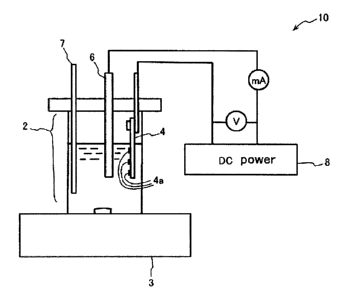
The electrolysis device shown in Figure 1, for example, may be used to conduct
the
electrolysis. In this figure, the electrolysis device (10) is equipped with an
electrolysis cell (2),
a magnetic stirrer (3), an cathode (4) comprising a semiconductor substrate, a
anode (6), a
thermometer (7) and a DC power source (8). An electrolysis solution containing
an organic
solvent is present inside the electrolysis cell (2). A metal catalyst (4a) is
unevenly formed on
the surface of the cathode (4) facing the anode (6). The electrolysis results
in electrolytic
deposition of carbon atoms from the organic solvent on the metal catalyst (4a)
and growth
toward the anode (6).
The nano carbon material electrolytically deposited may be mechanically peeled
from
the metal catalyst, for example, and recovered. In addition, nano carbon
materials
encapsulating the metal catalyst or nano carbon materials formed with the
metal catalyst on
the bottom may be obtained. Also, the nano carbon material may be used as it
is
electrolytically deposited on the semiconductor.
The conditions under which a nano carbon material is electrolytically
deposited are
shown schematically in Figures 2 and 3. In Figure 2, a metal catalyst (40a) is
formed in the
shape of islands on the surface of a semiconductor substrate (40), a nano
carbon material
extends toward the cathode (upward in the figure) from the edge of the metal
catalyst (40a)
by the edge effect described above and forms tubular carbon nanotubes. In
addition, in
Figure 3, an island-shaped metal catalyst (41a) is formed on the surface of a
semiconductor
substrate (41 ), and a nano carbon material is electrolytically deposited on
the entire surface
(including the side surface) of a metal catalyst (40a) forming a carbon onion
encapsulating
the metal catalyst.
Next, one embodiment of method for manufacturing a wiring structure of the
present
invention is explained. The method for manufacturing a wiring structure of the
present
invention is conducted using the same procedures used to manufacture the nano
carbon
materials described above, but the difference from the method described above
is the use of
a metal catalyst formed as protrusions from both ends of a wiring formation
location as the
anode and the cathode. In the method for manufacturing a wiring structure of
the present
CA 02530976 2005-12-29
8 PCT/JP03I16831
invention, a nano carbon material is formed as wiring on the metal catalyst
between the areas
acting as the anode and the cathode. This point will be explained with
reference to Figure 4.
In Figure 4, wiring patterns 200 and 201 [Figure 4(a)] are individually formed
on the
surfaces of two circuit substrates 100 and 101. Let us assume that the end
(right end) of the
wiring pattern 200 needs to be connected to the end (left end) of the wiring
pattern 201. In
this case, protrusions 200a and 201 a each comprising a metal catalyst are
already formed
along with the end of the wiring pattern 200 (right end) and the end of the
wiring pattern 201
(left end) forming both ends of the wiring formation location. Next, the
wiring formation
location described above containing at least the protrusions 200a and 201 a is
immersed (or
brought in contact) in an electrolysis solution containing an organic solvent.
In this case, the
entire individual circuit substrates 100 and 101 may be immersed, or an
electrolysis cell that
immerses only the wiring formation locations described above in the
electrolysis solution may
be used.
When an electrolysis is conducted using protrusions 200a and 201a as the
cathode
and anode, respectively (either may be the cathode but the protrusion 200a is
arbitrarily
designated as the cathode in this embodiment), under this condition, the nano
carbon
material electrolytically deposited on the protrusion 200a grows toward the
protrusion 201 a
and the nano carbon material connects to the protrusion 201a in due course.
The nano
carbon material forms a wiring 300 between protrusions 200a and 201a in the
manner
described. [Figure 4(b)] Now the electrolysis may be conducted using direct
current or an
alternating current electrolysis may be conducted. Actually, the protrusion
200a is electrically
conducted to the wiring pattern 200 and the protrusion 201 a is conducted to
the wiring pattern
201, the power source may be connected to the individual wiring patterns 200
and 201 for the
electrolysis. When a direct current electrolysis is conducted, an insoluble
metal or a carbon
material is preferably formed as an electrode on the protrusion on the anode
side.
The size (diameter) of protrusions 200a and 201a may be comparable to the size
(diameter) of the metal catalyst in the nano carbon material production method
described
above. By controlling the diameter, the same point at which the type of nano
carbon material
is changed in the nano carbon material production method described above is
observed. The
height of protrusions 200a and 201a may be, for example, several nm to several
10 nm.
Essentially, the current should be concentrated on protrusions 200a and 201a.
CA 02530976 2005-12-29
PCT/JP03/16831
Next, another embodiment of the wiring structure production method is
explained with
reference to Figure 5. In Figure 5, a protrusion 210a is formed on a wiring
pattern 210, and a
protrusion 211a is formed on a wiring pattern 211. Now the wiring patterns 210
and 211 are
positioned facing each other, and a wiring structure needs to be formed
between protrusions
210a and 211 a. Now in this figure, the wiring pattern 210 is positioned on
top of the wiring
pattern 211, and the protrusion 21 Oa is located on the extension of the
protrusion 211 a.
When a power source is connected to individual wiring patterns 210 and 211 and
an
electrolysis is conducted white at least the space between the protrusions
210a and 211a is
filled with the electrolysis solution described above, a nano carbon material
is formed in the
form of a wiring 301 between the protrusions 210a and 211a in the same manner
observed in
the Figure 4 described above. Now a nano carbon material forms a wiring
structure even
when it is slightly off from the extensions from the protrusions 21 Oa and 211
a.
As described above, a wiring structure can be formed at a low temperature such
as
ambient temperature and the like using a nano carbon material when a method
for
manufacturing a wiring structure of the present invention is used. In
addition, fine wiring
formation that was extremely difficult to obtain previously can be easily
conducted. That is, a
current concentrates on a protrusion in a wiring formation location, and a
nano carbon
material can be selectively electrolytically deposited on the areas where
wiring is desired.
(Examples)
Next, the present invention is explained in further detail by presenting
specific
examples below, but the present invention is not limited to these examples.
<Example 1 >
1. Metal Catalyst Formation on Semiconductor Surface.
Ni was spattered to a thickness of 30 nm on the surface of a semiconductor
substrate
(resistance ratio: 0.5 SZcm, electrode area 50 mm2) consists of p type
crystalline silicon and
was left standing for ten minutes in a gaseous ammonia atmosphere. This
treatment yielded
a semiconductor substrate from which a portion of the Ni was etched and
removed, leaving
granular Ni. The SEM (scanning electron microscope) image of the semiconductor
substrate
on which Ni was unevenly formed is shown in Figure 6. The white area in the
figure shows
granular Ni. The majority of the granular Ni was about 0.1 ~m to 0.5 ~m in
size (diameter),
CA 02530976 2005-12-29
PCT/JP03/16831
but the presence of granular Ni areas several 10 nm in diameter was also
confirmed when
the magnification of the SEM image was increased (not shown in the figures).
The
semiconductor substrate prepared using this etching method was labeled
substrate (1).
2. Electrolytic Deposition on cathode Using Electrolysis.
5 The electrolysis device shown in the aforementioned Figure 1 was prepared.
The
substrate (1) described above was used as the cathode. A carbon rod With an
external
diameter of 5 mm was used as the anode. Fifty milliliters of methane nitrite
(purity 99.5% by
volume, reagent special grade) was used as the electrolysis solution, and an
electrolysis was
conducted using a current density of 4 mA/cm2, a distance between electrodes
of 5 mm, an
10 electrolysis voltage of 1 kV and an electrolysis solution volume of 50 ml
to obtain an
electrolytically deposited material on the cathode surface. The electrolysis
was conducted at
room temperature, and the solution temperature rose only 2°C to
3°C after the electrolysis.
<Example 2>
In this example, the uneven deposition of Ni on the semiconductor substrate
described above and a nano carbon material electrolytic deposition were
conducted
simultaneously in the electrolysis solution described below.
First, 4.4 x 10⁻² mg of Ni nitrate was dissolved in 2.5 ml of ethanol (purity
99.5% by
volume, reagent special grade), and the solution was dissolved in 50 ml of
ethanol to prepare
an electrolysis solution. An electrolysis was conducted using electrolysis
conditions identical
to those described in Example 1 and an electrolytically deposited material was
obtained on
the cathode surface using the electrolysis solution and the electrolysis
device described
above, using the semiconductor substrate described above as the cathode and
the carbon
rod described above as the anode. The electrolysis time was eight hours. The
thinking is
that granular Ni was deposited on the semiconductor substrate in the initial
stage and a nano
carbon material was electrolytically deposited next on the Ni granules in this
electrolysis.
<Comparative Example>
An electrolysis was conducted and an electrolytically deposited material was
obtained
using the same procedure described in Example 1 above with the exception that
Ni was not
formed on the semiconductor substrate described above and ethanol was used as
the
electrolysis solution.
CA 02530976 2005-12-29
11 PCT/JP03/16831
The electrolytically deposited materials obtained in the individual examples
and the
comparative example were identified according to the following method. First
the SEM
(scanning electron microscope: manufactured by Nippon Denshi JSM-5600,
electron beam
15 kV) images of the cathode containing the electrolytically deposited
material obtained was
examined, and, in addition, TEM (transmittance type electron microscope:
manufactured by
Nippon Denshi, JEM-2010F, electron beam 200 kV) images of the electrolytically
deposited
material were examined. In addition, EDS (energy dispersive spectroscopy: an
energy
dispersing type X ray diffraction device, manufactured by Oxford, Link ISIS,
electron beam 15
kV) measurements were taken in the same measurement zone as the SEM
measurements
described above. The results are shown in Figures 7-18 and summarized in Table
1.
First, Figure 7 is an SEM image of the substrate surface obtained in Example 2
after
electrolytic deposition, Figure 8 is an partially enlarged view of the SEM
image of Figure 7,
Figure 9 is an partially enlarged view of the SEM image of Figure 8, Figure 10
is an partially
enlarged view of the SEM image of Figure 9. In each figure, white areas
represent deposited
materials and black areas represent accumulations of amorphous carbon films.
These
deposited materials showed spike-like (needle-like) growths using designated
sections of the
semiconductor substrate as the nucleus.
Figure 11 is an SEM image of another location on the substrate surface
obtained in
Example 2 after electrolytic deposition, and Figure 12 is an partially
enlarged view of the SEM
image of Figure 11. In each figure, white sections represent deposited
materials, and the
deposited materials show fibrous growths. Furthermore, an elemental analysis
was
conducted using EDX on the same measurement zones for the measurements shown
in
Figures 7 and 11 described above, and the white areas in individual figures
were found to be
carbon. The Figures 7 through 12 above indicate that fibrous carbon type
materials with a
diameter of about 100 nm are formed in Example 2, and they can be referred to
as carbon
nanowires.
Figure 13 is a TEM image of the electrolytically deposited material of Example
2. This
figure showed that an onion-shaped carbon material constructed from multiple
laminated
graphite layers was formed. In addition, the results of the EDX analysis
described above
indicated that the material was composed of carbon, and the conclusion was
that this
deposited material was a carbon onion.
CA 02530976 2005-12-29
12 PCT/JP03/16831
Figure 14 is a TEM image of the electrolytically deposited material of Example
2 in the
measurement zone different from that shown in Figure 13, and Figure 15 is an
partially
enlarged view of the TEM image of Figure 14. According to Figure 15, this
fibrous deposited
material contained multiple laminated layers of graphite with a hollow core.
According to
Figure 15, the distance between individual graphite layers was about 0.33 nm
to 0.36 nm, the
external diameter was about 30 nm and the internal diameter was about 2 nm.
The distance
between layers in carbon nanotubes is ordinarily 0.34 nm, and this deposited
material can be
identified as carbon nanotubes based on the data.
Figure 16 is an SEM image of the substrate surface from Example 1 after
electrolytic
deposition, and spikes of electrolytically deposited material using Ni as the
nucleus were
observed in the area slightly to the right of center of the figures. This
electrolytically
deposited material was also identified as carbon using EDX and was thought to
be carbon
nanowire.
Figure 17 is an SEM image of the substrate surface from the Comparative
Example
after electrolytic deposition, and the white and black areas in the figure
both represent
amorphous carbon film. The thinking is that the difference in the film
thickness (irregularity of
film surface) projects white and black areas. In addition, Figure 18 is an
partially enlarged
view of the SEM image of Figure 17. A film-like material was deposited over
almost the entire
substrate surface, but fibrous carbon materials such as carbon nanotubes,
carbon nanowires
and the like were not observed. Now this film-like material was examined using
Raman
spectroscopy, and no sharp signals associated with diamond-like carbon were
observed.
The thinking Was that the film was composed of amorphous carbon.
The results mentioned above are summarized in Table 1.
Table 1
State of ElectrolysisElectrol
metal ticall de
osited material
catal st solution Carbon nanotubeCarbon nanowireCarbon
onion
Example Uneven Methane Unconfirmed Present Unconfirmed
1
(etching nitrite
method
Example Uneven Ethanol Present Present Present
2
(electrolytic
method
Comp. None Methane Absent Absent Absent
Ex.
nitrite
CA 02530976 2005-12-29
13 PCT/JP03/16831
As clearly indicated by the data presented in Table 1, carbon nanotubes,
carbon
nanowires and carbon onions were obtained in Examples 1 and 2. In the case of
the
comparative example, amorphous carbon film layers were obtained, but no carbon
nanotubes
or carbon nanowires were obtained.
According to the method for manufacturing a nano carbon material of the
present
invention , a nano carbon material can be manufactured using a simple
electrolytic method
using a simple device and at a lower temperature (for example, ambient
temperature) than
previously used, and the method is particularly suited for manufacturing
fibrous nano carbon
materials such as carbon nanotubes, carbon nanowires and the like.