Note: Descriptions are shown in the official language in which they were submitted.
CA 02531155 2007-11-23
1
MORE COMPACT AND HIGHER RELIABILITY POWER SOURCE SYSTEM
FIELD OF THE IyVENTION
This invention relates to a compact, higher reliability power source system
for
supplyin~ low voltage DC power to computing loads from a high volta-e DC power
source.
BACKGROUND OF THE INVENTION
In a typical installation of a telecommunications system, data communications
system, computer equipment, servers, and the like, power is almost always
supplied by a
massive rechargeable storaje battery system with sufficient capacity to carry
the system
throu-
gh any power outages or interruptions. The battery system is completely
clamped
at the sum of individual cell voltacres and any primary power interruptions
are
completely bridged. Hence, anv powerline-frequency ripple coming from the
external
source is completely absorbed. The battery system can supply the equipment
with the
DC voltage and can completely isolate any equipment attached thereto from
utility
outages, ripple, and other problems with the external power source. Battery
drain is kept
small by a charginc, current that is continuously furnished from an external
high voltage
AC source, such as a utility main line or an uninterruptable power supply
(UPS). The
system chooses between the utility source or the UPS with a static transfer
switch. The
CA 02531155 2005-12-29
WO 2005/079520 PCT/US2005/005387
2
high voltage AC output from the static transfer switch is then input to a
transformer/rectifier device that supplies the needed charging current.
However,
conventional static transfer switches and transformer/rectifier devices
typically provide
no redundancy capabilities. Hence, failure of one of the components of these
devices
requires shutting the device down to replace the damaged component. Because
the
battery system is no longer being charged, it can sustain the system only for
a limited
number of hours, after which failure of the battery supplied power will
result.
Conventional battery systems typically distribute the DC power at voltages
close
to the final application voltages. Since losses are proportional to current
squared times
the resistance (IZIZ), keeping IZR losses down has required conventional
battery systems
to employ expensive, bulky, and not readily reconfigurable, bus-bar current
distribution
systems to carry the high current, low voltage DC power close to the point of
use.
In the past, the conventional battery based systems have been adequate.
However, the recent explosion in demand for data communications and computer
services makes the shortcomings of battery based systems clear. Prior battery
based
systems are expensive, massive, inflexible and occupy too much space.
Moreover, the
environmental hazards associated with the toxic waste created during battery
manufacturing and disposal are increasingly intolerable.
To date, high voltage DC power distribution has been impractical because of
the
lack of an economical and scalable DC-DC voltage down-converter. Very large
Ultra
HVDC converters have been in use for many years, but they require gigantic
installations and are completely unsuited to scaling down for the purpose of
distributing
DC power at common distribution voltages needed for a telecommunications
system or
a data communication system.,
CA 02531155 2005-12-29
WO 2005/079520 PCT/US2005/005387
3
SUMMARY OF THE INVENTION
It is therefore an object of this invention to provide a more compact and
higher
reliability power source system for computing loads.
It is a further object of this invention to provide such a power source system
that
provides low voltage DC without the need for a large and expensive central
battery
system.
It is a further object of this invention to provide such a power source system
which eliminates the need for a bulky, massive, inflexible and expensive bus-
bar current
distribution system.
It is a further object of this invention to provide such a power source system
in
the low voltage DC can be delivered close to the point of intended use.
It is a further object of this invention to provide such a power source system
which provides redundancy capabilities to improve reliability.
It is a further object of this invention to provide such a power source system
in
which the primary components of the system can be removed, replaced, or added
to the
system while the system is running.
It is a further object of this invention to provide such a power source system
in
which the primary components are hot swappable.
It is a further object of this invention to provide such a power source system
which improves the ratio of the distribution voltage to final application
voltage.
It is a further object of this invention to provide such a power source system
which is less expensive.
It is a further object of this invention to provide such a power source system
CA 02531155 2005-12-29
WO 2005/079520 PCT/US2005/005387
4
which utilizes less space.
It is a further object of this invention to provide such a power source system
which can easily be physically or electrically reconfigured.
It is a fizrther object of this invention to provide such a power source
system
which eliminates the toxic environmental problems associated with utilizing a
battery
based system.
This invention results from the realization that a more compact and higher
reliability power source system for providing low voltage DC voltage to
computing
loads can be effected by the unique combination of a high voltage DC bus that
is
connected to a number of DC sources that are each connected to the high
voltage DC
bus by a switch that delivers the DC source with the highest voltage to the
high voltage
DC bus, a low voltage DC bus connected to computing loads, and a power supply
that
includes a number of DC/DC converters connected in parallel between the high
voltage
DC bus and the low voltage DC bus that includes a controller for modulating
each of the
DC/DC converters to convert the high voltage on the high voltage DC bus to a
low
voltage DC output on the low voltage DC bus.
The subject invention, however, in other embodiments, need not achieve all
these objectives and the claims hereof should not be limited to structures or
methods
capable of achieving these objectives.
This invention features a more compact and higher reliability power source
system for computing loads, the system including a high voltage DC bus
connected to a
number of DC sources each connected to the high voltage DC bus by a switch
configured to deliver to the high voltage DC bus the DC source with the
highest DC
voltage, a low voltage DC bus connected to the computing loads, and a power
supply
CA 02531155 2007-11-23
including a number of DC/DC converters connected in parallel between the high
voltage
DC bus and the low voltage DC bus, and a controller configured to modulate
each
DC/DC converter to convert the high voltage on the high voltage DC bus to a
low
voltage output on the low voltage DC bus by utilizing pseudo-impedance to
provide
autonomous load sharing with other power supply modules.
In one embodiment, the switch may include a diode. The power supply may
include a plurality oi power supply modules each including a plurality of
DC/DC
converters and a controller. Each DC/DC converter may be configured as a buck
converter with a switch triggered by the controller to modulate the DC/DC
converter.
Each DC/DC converter may include an inverter, a transformer, and a rectifier
in which
the inverter is cycled by the controller to modulate the DCG'DC converter. The
controller
may be configured to modulate each DC/DC converter using modulation. The
controller may be configured to stagger the tiniing of the switch of each
DC/DC
converter to reduce ripple on the low voltage DC bus. The controller may be
responsive
to a fault signal input and progammed to open the switch of each DC/DC
converter in
response to a fault signal. The controller may be confiwred to stagger the
timing of the
inverter of each DC/DC converter to reduce ripple on the low voltage DC bus.
The
controller may be responsive to a fault signal input and progranimed to open
the inverter
of each DC/DC converter in response to a fault sipal. Each power supply module
may
include a fuse between the plurality of DC/DC converters and the low voltage
DC bus
designed to fail at a current level greater than the rated current output of
the power
supply module. The controller may be configured to determine a desired output
volta-e
based on the current output by the power supply module. The controller may
include a
switching voltage regulator configured to conipare a desired system output
voltage with
the voltage level output by the power supply module and to adjust the voltage
output of
CA 02531155 2005-12-29
WO 2005/079520 PCT/US2005/005387
6
each DC/DC converter such that the output of the power supply module
approximately
equals the desired system output voltage. The switching voltage regulator may
adjust
the voltage output by each of the DC/DC converters utilizing modulation. The
controller of each of the plurality of power supply modules may utilize pseudo-
impedance to provide autonomous load sharing of the plurality of power supply
modules. The low voltage output on the low voltage DC bus may be in the range
of
about 6V DC to 100V DC. The low voltage output on the low voltage DC bus
voltage
may be about 48V DC. The controller may be further configured to output an
error
signal in response to a fault signal. The controller may further include a
fault
determination circuit for generating the fault signal. Each of the plurality
of power
supply modules may include a cooling system. The fault detection circuit may
generate
a fault signal when a power supply module exceeds a predetermined temperature.
The
buck converter may include an input capacitor, an output capacitor, an
inductor, and the
switch. The ratio of the high voltage on the high voltage DC bus to the low
voltage on
the low voltage DC bus may be in the range 1.1:1 to about 1000:1. The ratio of
the high
voltage on the high voltage DC bus to the low voltage on the low voltage DC
bus may
be about 10:1. The ratio of the high voltage on the high voltage DC bus to the
low
voltage on the low voltage DC bus may be about 2:1. The power supply may be
housed
in a cabinet. Each of the plurality of power supply modules may be configured
as a
removable drawer. The removable drawers may be disposed in the cabinet. Each
removable drawer may include a plurality of different length connectors that
electrically
connect the number of DC/DC converters of the power supply module to the high
voltage DC bus at different times to reduce electrical discharge. Each of the
connectors
may include a resistive material therein for reducing electrical discharge
when
CA 02531155 2005-12-29
WO 2005/079520 PCT/US2005/005387
7
connecting the power supply module to the high voltage DC bus. Each removable
drawer may include an auxiliary contact connected by a separate auxiliary
resistor or
spark-suppressing impedance network for further reducing electrical discharge.
The
removable drawers may be able to be removed, replaced, or added while the
system is
running. Each drawer may include a number of cooling fans and exhaust ports
for
cooling the power supply modules. The components of each of the plurality of
power
supply modules may be arranged to maximize cooling efficiency. The computing
loads
may be chosen from the group consisting of: a telecommunications system, a
data
communication system, a computer systein, and computer peripherals. The power
supply may include a redundant number of power supply modules.
BRIEF DESCRIPTION OF THE DRAWINGS
Other objects, features and advantages will occur to those skilled in the art
from
the following description of a preferred embodiment and the accompanying
drawings, in
which:
Fig. 1 is a schematic block diagram of a typical conventional battery system
for
delivering low voltage DC to computing loads;
Fig. 2 is a schematic block diagram of one embodiment of the more compact and
higher reliability power source system of this invention;
Fig. 3 is a schematic block diagram showing the components of one embodiment
of the power supply shown in Fig. 2;
Fig. 4 is a schematic block diagram showing in detail the primary components
of
a power supply module shown in Fig. 3;
Fig. 5 is an electrical circuit diagram of a buck converter that may be
employed
CA 02531155 2005-12-29
WO 2005/079520 PCT/US2005/005387
8
in each of the DC/DC converters shown in Fig. 4;
Fig. 6 is an electrical circuit diagram of an inverter, transformer and
rectifier that
may be employed in each of the DC/DC converters shown in Fig. 4;
Fig. 7 is an electrical circuit diagram showing one embodiment of the
controller
shown in Fig. 4;
Fig. 8 is a graph showing the output V-I characteristic of the control circuit
shown fln Flg. 7;
Fig. 9 is a three-dimensional schematic view showing one example of the power
supply shown in Fig. 3 configured in a cabinet and the power supply modules
shown in
Fig. 4 configured as removable drawers in the cabinet;
Fig. 10 is a three-dimensional schematic view showing further details
associated
with the primary coinponents of a removable drawer shown in Fig. 9; and
Fig. 11 is a schematic three-dimensional view showing one example of the
connectors that may be used to connect the removable drawers shown in Fig. 9
to a high
voltage DC bus.
PREFERRED EIVIBODIMENT
Aside from the preferred embodiment or embodiments disclosed below, this
invention is capable of other embodiments and of being practiced or being
carried out in
various ways. Thus, it is to be understood that the invention is not limited
in its
application to the details of construction and the arrangements of components
set forth
in the following description or illustrated in the drawings. If only one
embodiment is
described herein, the claims hereof are not to be limited to that embodiment.
Moreover,
the claims hereof are not to be read restrictively unless there is clear and
convincing
CA 02531155 2005-12-29
WO 2005/079520 PCT/US2005/005387
9
evidence manifesting a certain exclusion, restriction, or disclaimer.
As discussed in the Background section above, conventional power source
system 10, Fig. 1, utilizes large battery system 12 to provide low voltage DC,
e.g., 48V
DC, to computing loads 14, such as data communications equipment, computer
systems,
and the like. System 10 typically includes static transfer switch 16
responsive to a high
voltage AC source on line 18 delivered by a conventional utility line or a
high voltage
AC source delivered by a UPS or similar device on line 20 in the event of a
power
failure. Static transfer switch 16 delivers either the high voltage AC source
from the
utility line or the UPS by line 17 to transformer/rectifier device 22.
Transformer/rectifier device 22 provides the necessary charging current to
continually
charge the batteries in battery system 12. However, as discussed above,
battery system
12 and its associated high current, low voltage DC bus 13 are typically
massive in size.
Moreover, system 10 provides no redundancy for any of the components for
static
transfer switch 16 or transformer/rectifier device 22.
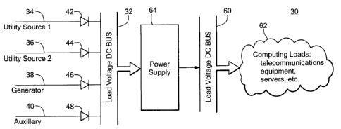
In contrast, a more compact and higher reliability power source system 30,
Fig. 2
in accordance with this invention, includes high voltage DC bus 32 connected
to a
number of high voltage DC sources, such as DC source 34 (e.g., utility source
1), DC
source 36 (e.g., utility source 2), DC source 38 (e.g., a generator), and DC
source 40
(e.g., an auxiliary source). High voltage DC sources 34-40 are typically at
about
550V DC. DC sources 34-40 are each connected to high voltage DC bus 32 with a
switch, e.g., a diode, that is configured to deliver to high voltage bus 32
power from the
DC source with the highest DC voltage. In this example, switches 42, 44, 46
and 48
connect DC sources 34, 36, 38 and 40, respectively, to high voltage DC bus 32.
In
operation, when the voltage on any of DC sources 34-40 is greater than the
voltage on
CA 02531155 2005-12-29
WO 2005/079520 PCT/US2005/005387
high voltage DC bus 32, the switch (diode) associated with the DC source with
the
highest voltage is forward biased and the high voltage DC voltage will be
supplied from
that source. The switches for the remaining DC sources will be back-biased by
the
small negative differential voltages deliberately or accidentally introduced
between the
voltages from those sources and voltage of the highest-voltage source, and
hence no
power will be delivered by those sources. If, however, the active source fails
or its
voltage drops below any of the other power sources, power will instantaneously
and
automatically be drawn from the new highest voltage source. High voltage DC
bus 32 is
typically distributed throughout a typical installation of system 30 and
provides for
connecting power supply 64 close to the point of intended use (discussed
below).
System 30 also includes low voltage DC bus 60 connected to computing
loads 62, e.g., telecommunications equipment, data communications equipment,
computer equipment, servers, and the like, or any electronic device or system
that
utilizes low voltage DC. Typically, the voltage on low voltage DC bus 60 is in
the
range of about 6V DC to 100V DC, e.g., about 48V DC.
Power supply 64 includes a number of DC/DC converters (discussed below)
connected in parallel between high voltage DC bus 32 and low voltage DC bus 60
and a
controller (also discussed below) configured to modulate each DC/DC converter
to
convert the high voltage on high voltage DC bus 32 to a low voltage output on
low
voltage DC bus 60.
In a preferred embodiment, power supply 64, Fig. 3, includes a plurality of
power supply modules, e.g., power supply modules 66, 68, 70, 72, 74, and 76
that each
include a plurality of DC/DC converters and a controller. For example, each
power
supply module 66-76 includes DC/DC converters 150, 152, 154, 156, 158 and 160,
CA 02531155 2005-12-29
WO 2005/079520 PCT/US2005/005387
11
Fig. 4, that are connected in parallel between high voltage DC bus 32 and low
voltage
DC bus 60. Connector 81 connects the high voltage DC on line 101 from high
voltage
bus 32 to each of DC/DC converters 150-160 by lines 103, 105, 107, 109, 111,
and 113,
respectively. Controller 80 modulates each of DC/DC converters 150-160 by
lines 220,
222, 224, 226, 228 and 230 to convert the high voltage DC on lines 103-113 to
low
voltage DC on lines 96, 98, 100, 102, 104 and 106. Connector 117 connects the
output
of DC/DC converters 150-160 on lines 96-106 to line 90.
The result is that low voltage DC is supplied to low voltage DC bus 60, Fig.
2,
without the need for a massive and cumbersome battery system. Each of power
supply
modules 66-76, Fig. 3 are relatively small in size, e.g., 19" by 5" by 24",
for a typica130
kW power supply module, which results in power supply 64 being compact.
Because
power supply 64 is compact and utilizes high voltage DC from high voltage DC
bus 32
that can be distributed throughout an installation of system 30, power supply
64 can be
located close to the point of intended use. Hence, the need for a large and
expensive
low-voltage, high-current bus-distribution system is eliminated. This allows a
higher
ratio of the DC voltage on the high voltage DC bus 32 to final application
voltage on
low voltage DC bus 60 that is the range of about 1.1:1 to 1000:1, e.g., 10:1
or 2:1. A
higher bus voltage translates through Ohm's law to a proportionally lower
current for
the same power. Using a higher voltage input power bus distribution system
(high
voltage DC bus 32) therefore reduces IaR losses in the high voltage bus 32,
which
further reduces energy usage and costs. System 30 can also utilize a number of
independent high voltage DC sources discussed above and automatically uses the
DC
source with the highest DC voltage, which improves the reliability. System 30
also has
redundancy capabilities (discussed below) which provide increased
uninterruptability
CA 02531155 2005-12-29
WO 2005/079520 PCT/US2005/005387
12
and reliability. System 30 can also be relocated as needed, and can be
connected in
parallel with any number of power source systems 30 as needed to meet any
changing
load physical configurations or electrical requirements.
In one design, fuse 119, Fig. 4, is connected between the output voltage of
the
power supply module on line 90 and the low voltage DC bus by line 121. Fuse
119 is
designed to fail when the current level output by the power supply module is
greater
than the rated current output of the power supply module, e.g., 600 amps.
Each of the DC converters 150-160, Fig. 4 is typically configured as a buck
converter, as shown by buck converter 84, Fig. 5. Buck converter 84 includes
input
capacitor 210, diode 212, inductor 214 and output capacitor 216 and switch 86,
e.g., an
insulated gate bipolar transistor (IGBT). Switch 86 is triggered by controller
80, Fig. 4,
to modulate the voltage output of the buck converter of each of DC/DC sources
150-160
and convert the high voltage DC on lines 103-113 to low voltage DC on lines 98-
106.
For example, controller 80 may utilize fixed clock modulation, e.g., pulse
width
modulation, to generate pulse width signals on lines 220-230 that time how
long each
switch of each buck converter of DC/DC converters 150-160 will remain open and
closed in order to adjust the ratio of the "on" time and "off' time of the
switch of the
buck converter to control the output voltage and effectively convert the high
voltage DC
on lines 103-113 to low voltage DC on lines 96-106 and control the output
voltage of
the power supply module on line 90. Controller 80 may utilize fixed clock
modulation,
e.g., pulse width modulation, self-oscillation modulation, e.g., pulse
frequency
modulation or hysteretic modulation, or any type of modulation known to those
skilled
in the art, to control the timing of the switches in DC/DC 150-160 to convert
the high
voltage DC to low voltage DC.
CA 02531155 2005-12-29
WO 2005/079520 PCT/US2005/005387
13
In one design, each of DC/DC converters 150-160 is configured as shown in
Fig. 6. In this example, each of DC/DC converters 150-160, Fig. 4 includes
inverter
250, Fig. 6, transfonner 252 and rectifier 254. Similar to the switch in the
buck
converter described above, inverter 250 is triggered by controller 80, Fig. 4
to modulate
each of DC/DC converters 150-160 and convert the high voltage DC on lines 103-
113,
Fig. 4 to the low voltage DC on lines 98-106.
In a preferred embodiment, controller 80 initiates the signals on lines 220-
230
that are equally time staggered, e.g., staggered 60 apart in phase for the
six parallel DC-
DC sources 150-160, or 360 /N for N parallel units, to stagger the timing of
the switch
or inverter in each of DC/DC sources 150-160 described above to reduce the
ripple of
the low voltage DC on line 90.
Controller 80 can also determine a desired output voltage to be output by the
power supply module on line 90 based on the current output by the power supply
module by feedback line 93. Controller 80 includes switching voltage regulator
92 that
compares the desired system output voltage on low voltage DC bus 60 by
feedback line
95 with the actual voltage output by the power supply module on line 90.
Switching
voltage regulator 92 then adjusts the voltage output of the power supply
module to the
desired system voltage output by changing the modulation of DC/DC converters
150-
160 using fixed clock modulation (e.g., pulse width modulation), self-
oscillating
modulation, e.g., pulse frequency modulation or hysteretic modulation, or any
modulation technique known to those skilled in the art.
In one embodiment, controller 80 is also responsive to a fault signal on
feedback
line 93 and is programrned to open the switch (e.g., switch 86, Fig. 5), or
inverter (e.g.,
inverter 250, Fig. 6) of each of the DC/DC converters 150-160, Fig. 4, when
the fault
CA 02531155 2005-12-29
WO 2005/079520 PCT/US2005/005387
14
signal on line 93 indicates the power supply module is generating excessive
voltage or
current (discussed in detail below). This will remove the malfunctioning power
supply module from the parallel configuration of power supply modules 66-76,
Fig. 3 of
power supply 64 and hence prevent the damaged power supply module from
effecting
the operation of power supply 64. Controller 80, may also generate an error
signal on
line 108 that enables an external controller, such as a PLC, in response to
the fault signal
on line 112 from the various subsystems within the power supply module. For
example,
fault determination circuitry 110 may be responsive to cooling system 113 that
detects
an overheating condition in the power supply module and thus activates fault
determination circuitry 110 to generate a fault signal on line 112 that
enables controller
80 to generate an error signal on line 108 to enable the external controller.
Additional
auxiliary system 114 can also generate an error signal on line 116 that
enables fault
determination circuitry 110 to generate a fault signal on line 112 and enable
controller
80 to generate an error signal to enable the external controller.
Fig. 7, where like parts have been given like numbers, shows one embodiment of
controller 80 of this invention that utilizes pulse width modulation to adjust
the low
voltage DC output of each of power supply modules 66-76, Fig. 3. In this
example,
comparator 119, Fig. 7 compares a reference system output voltage, Vset,
indicated at
120, e.g., the voltage on the low voltage DC bus discussed above, to the
measured
output voltage of the power supply module, Vmeasa indicated at 122, and
generates an
error signal on line 124. Controller 80 also includes comparator 139 that
measures the
output current of the power supply module, Ieav indicated at 126. The measured
current, Imeas on line 140, can take one path through large resistor 143,
e.g., about
150kn, and is combined with the error signal on line 124 to provide a trimmed
and
CA 02531155 2005-12-29
WO 2005/079520 PCT/US2005/005387
adjusted error signal on line 130 that provides only a slight change in the
voltage output
of the power supply module. This adjustment causes the output voltage of the
power
supply module to shift over a narrow range of values and is used to vary the
output
voltage of the power supply module to create the effect of a small positive
internal
impedance. The trimmed and adjusted signal on line 130 establishes a synthetic
V-I
characteristic, as shown by curve 169, Fig. 8. The trimmed and adjusted signal
provides
the power supply module with an apparent, battery-like source-resistance or
"pseudo-
impedance" corresponding to a small, but positive value of internal
resistance, indicated
by arrow 190 that enables the power supply module, e.g., power supply module
66, Fig.
3, to share loads equally with the other power supply modules, e.g., power
supply
modules 68-76 of power supply 64.
The measured current, Imeasa indicated at 126, Fig. 7, also takes another path
on
line 180 that includes zener diode 182 and small resistor 184, e.g., about
301n. During
operation, zener diode 182 remains off. However, if higher than allowable
current
begins to be drawn by the power supply module, the current, Imeas, increases
and zener
diode 182 will be enabled. At this point, small resistor 184 strongly drags
the signal
voltage down. This results in a large and rapid change in the trimmed and
adjusted error
signal on line 130 and a radical reduction in the commanded local output
voltage set
point. The result is a sudden and steep drop-off of the V-I curve 169, Fig. 8,
as
indicated by arrow 194. This feature guarantees that if the current of an
individual
power supply module starts to become too high, the output voltage of power
supply
module will drop rapidly and shut that power supply module down.
Switching voltage regulator 92, Fig. 7 is responsive to the trimmed and
adjusted
error signal on line 130 and adjusts the output voltage generated by each of
the DC/DC
CA 02531155 2005-12-29
WO 2005/079520 PCT/US2005/005387
16
converters 150-160, Fig. 4, using modulation, e.g., fixed clock modulation,
such as
pulse width modulation (although any type of modulation as discussed above may
be
utilized). Switching voltage regulator 92 typically includes voltage
controlled delay
generator 134, processor 145, switch 162, e.g., a FET, capacitor 164, pull-up
resistor
166 and voltage source 168. In operation, voltage controlled delay generator
134 is held
in an inhibited state by the voltage on capacitor 164. Discharging of
capacitor 164
enables voltage controlled delay generator 134 to process the trimmed and
adjusted error
signal on line 130 to enable processor 145 by line 143. Discharging of
capacitor 164 is
achieved by a reset signal on line 163 that enables FET 162 to discharge
capacitor 164
by ground 169. Charging of capacitor is achieved by voltage source 168, as
known by
those skilled in the art. The trimmed and adjusted error signal on line 143
enables
processor 145 to generate pulse width signals on lines 220-230, indicated by
arrow 170,
to control the timing of the switches of DC/DC converters 150-160, Fig. 4, as
discussed
above. Based on the size of error signal on line 130, processor 145 determines
the pulse
width that is needed by the signals on lines 220-230 to control the timing of
the switch
of each of DC/DC converters 150-160, Fig. 4, to adjust the output voltage of
the power
supply module to the desired system output voltage. Processor 145, Fig. 7,
also
determines the sequencing of the pulse signals on lines 220-230 to stagger the
triggering
of the switches or inverters of DC/DC converters 150-160 to reduce ripple. For
example, processor 145, can initiate a sequence of pulses, shown by arrow 170,
that
stagger the triggering of the switches or inverters of the six DC/DC
converters 150-160,
Fig. 4, to reduce ripple. Typically, the staggered pulse signals on lines 220-
230 are in a
time staggered sequence 60 apart in phase for the six DC sources 150-160, as
described
above.
CA 02531155 2005-12-29
WO 2005/079520 PCT/US2005/005387
17
The "pseudo" impedance described above in relation to controller 80, Figs. 4,
7,
and 8 provides desirable load sharing of power supply modules 66-76, Fig. 3.
In this
embodiment, if an individual power supply module of power supply modules 66-
76, of
power supply 64 is lightly loaded compared to the other power supply modules,
that
power supply module will operate at a slightly higher output voltage (due to
its positive
"pseudo-impedance"). Conversely, the output voltage for an individual power
supply
module of power supply modules 66-76 will be slightly lower when a heavier
current is
being drawn from it. The higher voltages of lightly loaded power supply
modules will
result in more current being drawn from them, which will have the effect of
reducing
their output voltage. The more highly loaded power supply modules will draw
less
currents, increasing their output voltage. In this way, all of the modules
will reach an
equilibrium in the middle of the voltage range, in which power is drawn
equally from
each module, without any explicit control signals required to be passed
between the
modules. This process of continuous mutual load adjustment and load sharing
guarantees overall system stability, and prevents any one supply (or
collection of
supplies) from "hogging" the load.
In a preferred embodiment, power supply 64, Figs. 2 and 3, is ideally enclosed
in
a cabinet, such as cabinet 300, Fig. 9. Power supply modules 66-76, Fig. 3,
are typically
each enclosed in a removable drawer, such as drawer 302, Fig. 9. Removable
drawer
302 houses the various components of the individual power supply modules 66-76
discussed above in reference to Fig. 4. For example, drawer 302, Fig. 10,
includes six
DC/DC converters, of which three are shown and three are stacked below (not
shown).
The inductors of the buck converters of the shown DC/DC converters are
indicated at
310, 312, and 314. The IGBT switch for each of the three buck converters is
indicated
CA 02531155 2005-12-29
WO 2005/079520 PCT/US2005/005387
18
at 316, 318 and 320. The input capacitors are indicated at 322, 324, and 326.
The
controller (shown in phantom) is indicated at 326. Drawer 302 typically
includes
cooling fans 330 that provide cooling air to drawer 302 that exits through
exhaust ports
(not shown) located on back pane1332. The orientation of inductors 310-314,
switches
316-320 and input capacitors 322-326 are arranged to maximize the cooling
efficiency
of drawer 302.
Drawer 302 typically includes a plurality of different length connectors,
e.g.,
connectors 340, 342, 344, and 346, Fig. 11, that allow the DC/DC converters to
be
connected to the high voltage DC bus without causing electrical discharge. In
one
example, each of the connectors 340-348 may include a section of resistive
material,
such as resistive material 352 in connector 346 to prevent discharge of high
voltage DC
when connecting drawer 302 to the high voltage DC bus. In some designs an
auxiliary
contact connected by a separate auxiliary resistor or spark-suppressing
impedance
network may be employed to further prevent discharge of high voltage DC when
connecting drawer 302 to the high voltage DC bus. Hence, the configuration of
connectors 340-348 allows each of the various removable drawers that house the
power
supply modules to be added, removed, or replaced while a system 30 is in
operation, i.e.,
the removable drawers are "hot swappable".
Although specific features of the invention are shown in some drawings and not
in others, this is for convenience only as each feature may be combined with
any or all
of the other features in accordance with the invention. The words "including",
"comprising", "having", and "with" as used herein are to be interpreted
broadly and
comprehensively and are not limited to any physical interconnection. Moreover,
any
embodiments disclosed in the subject application are not to be taken as the
only possible
CA 02531155 2005-12-29
WO 2005/079520 PCT/US2005/005387
19
embodiments. Other embodiments will occur to those skilled in the art and are
within
the following claims.
In addition, any amendment presented during the prosecution of the patent
application for this patent is not a disclaimer of any claim element presented
in the
application as filed: those skilled in the art cannot reasonably be expected
to draft a
claim that would literally encompass all possible equivalents, many
equivalents will be
unforeseeable at the time of the amendment and are beyond a fair
interpretation of what
is to be surrendered (if anything), the rationale underlying the amendment may
bear no
more than a tangential relation to many equivalents, and/or there are many
other reasons
the applicant can not be expected to describe certain insubstantial
substitutes for any
claim element amended.
What is claimed is: