Language selection

Search

Patent 2531252 Summary

Third-party information liability

Some of the information on this Web page has been provided by external sources. The Government of Canada is not responsible for the accuracy, reliability or currency of the information supplied by external sources. Users wishing to rely upon this information should consult directly with the source of the information. Content provided by external sources is not subject to official languages, privacy and accessibility requirements.

Claims and Abstract availability

Any discrepancies in the text and image of the Claims and Abstract are due to differing posting times. Text of the Claims and Abstract are posted:

  • At the time the application is open to public inspection;
  • At the time of issue of the patent (grant).
(12) Patent: (11) CA 2531252
(54) English Title: VOLTAGE SENSING APPARATUS FOR MEDIUM-VOLTAGE ELECTRICAL POWER DISTRIBUTION SYSTEMS
(54) French Title: APPAREIL DE MESURE DE LA TENSION POUR RESEAUX DE DISTRIBUTION D'ELECTRICITE A MOYENNE TENSION
Status: Granted
Bibliographic Data
(51) International Patent Classification (IPC):
  • G01R 15/06 (2006.01)
  • G01R 19/32 (2006.01)
(72) Inventors :
  • MULLIGAN, TIMOTHY J. (United States of America)
  • BARKER, JAMES W., JR. (United States of America)
(73) Owners :
  • S&C ELECTRIC COMPANY (United States of America)
(71) Applicants :
  • S&C ELECTRIC COMPANY (United States of America)
(74) Agent: OSLER, HOSKIN & HARCOURT LLP
(74) Associate agent:
(45) Issued: 2014-11-04
(22) Filed Date: 2005-12-21
(41) Open to Public Inspection: 2006-06-28
Examination requested: 2010-09-08
Availability of licence: N/A
(25) Language of filing: English

Patent Cooperation Treaty (PCT): No

(30) Application Priority Data:
Application No. Country/Territory Date
60/639,260 United States of America 2004-12-28

Abstracts

English Abstract

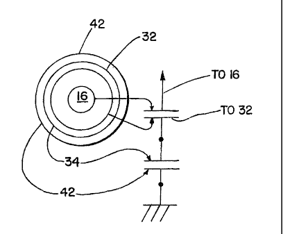
A molded voltage sensor is provided that achieves excellent sensing accuracy over a wide temperature range by molding primary and secondary capacitances of a voltage divider into a solid dielectric material and wherein the capacitances are preferably fabricated from the same material, or at least materials having nearly identical temperature coefficients of permittivity. In a preferred arrangement, a first member of dielectric material includes a conductive pattern on the outer surface thereof and an electrical connection attached to the conductive pattern. The first member is then molded into a predetermined location with respect to a central conductor and a layer of the dielectric molding material is also molded over the exterior of the first member. Another conductive pattern is formed on the over-molded layer. The overall assembly is then molded to form a body of the desired shape and provides insulation between the conductor and the conductive patterns.


French Abstract

Un capteur de tension moulé est fourni et obtient une excellente précision de détection sur une grande plage de températures en moulant des capacitances primaires et secondaires dun diviseur de tension en un matériau diélectrique solide et dans lequel les capacitances sont de préférence fabriquées du même matériau, ou au moins de matériaux qui présentent des coefficients de température de résistivité presque identiques. Dans une disposition préférée, un premier élément de matériau diélectrique comprend une impression conductrice sur la surface extérieure de celui-ci et une connexion électrique fixée à limpression conductrice. Le premier élément est ensuite moulé dans un endroit prédéterminé par rapport à un conducteur central et une couche du matériau de moulage diélectrique est également moulée sur lextérieur du premier élément. Une autre impression conductrice est formée sur la couche surmoulée. Lensemble total est ensuite moulé pour former un corps de la forme souhaitée et procure une isolation entre le conducteur et les impressions conductrices.

Claims

Note: Claims are shown in the official language in which they were submitted.


The embodiments of the present invention for which an exclusive property or
privilege is
claimed are defined as follows:
1. A voltage sensor comprising voltage divider capacitors being formed
within a
molded body comprising:
a first member of dielectric material being of generally cylindrical shape and

having a first conductive pattern formed on the exterior thereof and an
interconnection
facility extending therefrom;
a conductor arranged to extend through the first member;
a molded body of similar dielectric material defined about the conductor and
the
first member with a second conductive pattern being formed on the exterior of
the
molded body adjacent the first member and the interconnection facility
extending to the
exterior of the molded body; and
an outer body being formed about the molded body, a first voltage divider
capacitor being formed between the conductor and the first conductive pattern,
a second
voltage divider capacitor being formed between the first and second conductive
patterns.
2. The voltage sensor of claim 1 wherein said first member, said molded
body and
said outer body all being the same material.
-4-

Description

Note: Descriptions are shown in the official language in which they were submitted.


CA 02531252 2005-12-21
VOLTAGE SENSING APPARATUS FOR MEDIUM-VOLTAGE
ELECTRICAL POWER DISTRIBUTION SYSTEMS
BACKGROUND OF THE INVENTION
1. Field of the Invention
The present invention relates generally to sensors for the electrical power
distribution
field and more particularly to a molded voltage sensor that achieves excellent
sensing accuracy
over a wide temperature range.
2. Description of Related Art
Various voltage sensing arrangements are known in the electrical power
distribution field
that utilize molding technology. For example, see the following U.S. Patent
Nos.: 6,031,368;
6,538,422; 5,438,161; 5,162,726; and 4,002,976.
While the prior art arrangements may be useful, it would be desirable to
provide a voltage
sensor that achieves excellent sensing accuracy over a wide temperature range.
SUMMARY OF THE INVENTION
Accordingly, it is a principal object of the present invention to provide a
voltage sensor
that achieves excellent sensing accuracy over a wide temperature range.
It is another object of the present invention to provide a molded voltage
sensor that
provides accurate sensing over a wide temperature range via a fabrication
process.
It is a further object of the present invention to provide a molded voltage
sensor that is
fabricated utilizing several molding steps of the same materials (or materials
of similar
coefficients of thermal expansion) thus avoiding internal stress problems
while achieving
accurate sensing over a wide temperature range.
These and other objects of the present invention are efficiently achieved by
the provision
of a molded voltage sensor that achieves excellent sensing accuracy over a
wide temperature
range by molding primary and secondary capacitances of a voltage divider into
a solid dielectric
material and wherein the capacitances are preferably fabricated from the same
material, or at
least materials having nearly identical temperature coefficients of
permittivity. In a preferred
arrangement, a first member of dielectric material includes a conductive
pattern on the outer
surface thereof and an electrical connection attached to the conductive
pattern. The first member
is then molded into a predetermined location with respect to a central
conductor and a layer of
the dielectric molding material is also molded over the exterior of the first
member. Another

CA 02531252 2005-12-21
conductive pattern is formed on the over-molded layer. The overall assembly is
then molded to
form a body of the desired shape and provides insulation between the conductor
and the
conductive patterns.
BRIEF DESCRIPTION OF THE DRAWING
The invention, both as to its organization and method of operation, together
with further
objects and advantages thereof, will best be understood by reference to the
specification taken in
conjunction with the accompanying drawing in which:
FIG. 1 is an elevational view, partly in section, of a voltage sensor
fabricated in
accordance with the present invention;
FIG. 2 is a front elevational view of an inner member of the voltage sensor of
FIG. 1;
FIG. 3 is a sectional view taken generally along the line 3-3 of FIG. 2;
FIG. 4 is an enlarged view of a portion of the inner member of FIG. 2;
FIG. 5 is a front elevational view of an intermediate molding step of portions
of the
voltage sensor of FIG. 1;
FIG. 6 is a sectional view taken generally along the line 6-6 of FIG. 5; and
FIG. 7 is a diagrammatic representation and schematic representation of the
voltage
divider formed within the voltage sensor of FIG. 1.
DETAILED DESCRIPTION
Referring now to FIG. 1, a voltage sensor 10 fabricated in accordance with the
principles
of the present invention includes a molded outer body or housing 12
incorporating an inner
member 14 forming a first capactive plate or capacitance with respect to an
inner conductor 16
extending through the body 12 and within the inner member 14. The output of
the voltage sensor
10 is provided via a conductor 18 connected to the inner member 14, e.g. the
conductor 18 is a
coaxial cable 20 having a shield 22 about the inner conductor 18.
Referring now to FIGS. 2-4, the inner member 14 is fabricated from a suitable
dielectric,
e.g. molded or fabricated from cycloaliphatic epoxy resin. The inner member 14
has an inner
diameter 32 to accommodate the conductor 16 and an outside diameter 34 to
result in suitable
capacitance for the voltage sensor 10 as will be explained in more detail
hereinafter. The inner
member 14 is then appropriately prepared, e.g. by sandblasting, and then
coated with a
conductive paint to provide a conductive coating at 34, preferably, the inner
diameter 32 also
being coated to alleviate electrical stress and to maintain desirably high
capacitance values of the
voltage sensor 10. The inner member 14 also includes facilities at 36 for
attachment of a suitable
- 2 -

CA 02531252 2013-09-06
conductor to the conductive coating at 34. For example, and referring now to
FIG. 5, the inner
conductor 18 of the coaxial cable 20 is connected to the conductive coating 34
via the connector
at 36.
Considering now the further fabrication of the voltage sensor 10 and referring
now to
FIG. 6, the conductor 16 is molded within the inside diameter of the inner
member 14, and
simultaneously, the inner member 14 is also encapsulated in a layer of the
same material as the
inner member 14, e.g. the encapsulation of the inner member about the
conductor 16 resulting in
the defining of an outer member 40 with a predetermined thickness 41 on the
outer surface of the
inner member 14 to define a suitable capacitance. Further, to facilitate
accurate location of the
inner member 14 in the molding process and thereby control the thickness of
the outer surface
41, recesses 43 (FIGS. 3 and 6) are provided into the surface of the inner
member 14. Portions
of the outer surface of the encapsulation 40 are prepared, e.g. by
sandblasting, and then
conductive paint is applied in predetermined areas, e.g. at 42, to form a
conductive pattern and
forming a capacitor with respect to the conductive coating at 34 on the outer
diameter of the
inner member 14. As seen in FIG. 1, the shield 22 of the coaxial cable 20 is
connected to the
area 42 of conductive coating via a wire 44 and a garter spring 46 positioned
about the
encapsulation 40 and retained within a groove 48 formed in the encapsulation
40, e.g. during the
forming thereof. A second groove 50 is formed in the encapsulation 40 to
accept a second garter
spring 52, the springs 46 and 52 providing a shield function to the edge of
the conductive coating
of areas 42.
As shown in FIG. 1, the overall assembly as described thus far is then molded
to form the
overall body 12 in the desired overall shape for application as the voltage
sensor 10. In a
preferred embodiment, the body 12 is formed from the same material as the
inner member 14 and
the encapsulation 40. The body 12 also provides insulation between the
conductor 16 and the
outer conductive coating at 42 of the formed outer member 40. During the
molding of the body
12, the conductor 18 of coaxial cable 20 is directed to the outside of the
body 12 to provide the
output of the voltage sensor 12 with respect to ground. A schematic
representation of the voltage
divider formed within the voltage sensor 10 is illustrated in FIG. 7.
While there have been illustrated and described various embodiments of the
present
invention, it will be apparent that various changes and modifications will
occur to those skilled in
the art. The scope of the claims should not be limited by the preferred
embodiments set forth in
the examples, but should be given the broadest interpretation consistent with
the description as a
whole.
- 3 -

Representative Drawing
A single figure which represents the drawing illustrating the invention.
Administrative Status

For a clearer understanding of the status of the application/patent presented on this page, the site Disclaimer , as well as the definitions for Patent , Administrative Status , Maintenance Fee  and Payment History  should be consulted.

Administrative Status

Title Date
Forecasted Issue Date 2014-11-04
(22) Filed 2005-12-21
(41) Open to Public Inspection 2006-06-28
Examination Requested 2010-09-08
(45) Issued 2014-11-04

Abandonment History

There is no abandonment history.

Maintenance Fee

Last Payment of $473.65 was received on 2023-12-15


 Upcoming maintenance fee amounts

Description Date Amount
Next Payment if standard fee 2024-12-23 $624.00
Next Payment if small entity fee 2024-12-23 $253.00

Note : If the full payment has not been received on or before the date indicated, a further fee may be required which may be one of the following

  • the reinstatement fee;
  • the late payment fee; or
  • additional fee to reverse deemed expiry.

Patent fees are adjusted on the 1st of January every year. The amounts above are the current amounts if received by December 31 of the current year.
Please refer to the CIPO Patent Fees web page to see all current fee amounts.

Payment History

Fee Type Anniversary Year Due Date Amount Paid Paid Date
Application Fee $400.00 2005-12-21
Registration of a document - section 124 $100.00 2007-02-05
Expired 2019 - The completion of the application $200.00 2007-02-05
Maintenance Fee - Application - New Act 2 2007-12-21 $100.00 2007-12-21
Maintenance Fee - Application - New Act 3 2008-12-22 $100.00 2008-12-12
Maintenance Fee - Application - New Act 4 2009-12-21 $100.00 2009-12-10
Request for Examination $800.00 2010-09-08
Maintenance Fee - Application - New Act 5 2010-12-21 $200.00 2010-09-08
Maintenance Fee - Application - New Act 6 2011-12-21 $200.00 2011-12-13
Maintenance Fee - Application - New Act 7 2012-12-21 $200.00 2012-12-17
Maintenance Fee - Application - New Act 8 2013-12-23 $200.00 2013-12-13
Final Fee $300.00 2014-08-15
Maintenance Fee - Patent - New Act 9 2014-12-22 $200.00 2014-12-15
Maintenance Fee - Patent - New Act 10 2015-12-21 $250.00 2015-12-14
Maintenance Fee - Patent - New Act 11 2016-12-21 $250.00 2016-12-19
Maintenance Fee - Patent - New Act 12 2017-12-21 $250.00 2017-12-18
Maintenance Fee - Patent - New Act 13 2018-12-21 $250.00 2018-12-17
Maintenance Fee - Patent - New Act 14 2019-12-23 $250.00 2019-12-13
Maintenance Fee - Patent - New Act 15 2020-12-21 $450.00 2020-12-11
Maintenance Fee - Patent - New Act 16 2021-12-21 $459.00 2021-12-17
Maintenance Fee - Patent - New Act 17 2022-12-21 $458.08 2022-12-16
Maintenance Fee - Patent - New Act 18 2023-12-21 $473.65 2023-12-15
Owners on Record

Note: Records showing the ownership history in alphabetical order.

Current Owners on Record
S&C ELECTRIC COMPANY
Past Owners on Record
BARKER, JAMES W., JR.
MULLIGAN, TIMOTHY J.
Past Owners that do not appear in the "Owners on Record" listing will appear in other documentation within the application.
Documents

To view selected files, please enter reCAPTCHA code :


To view images, click a link in the Document Description column. To download the documents, select one or more checkboxes in the first column and then click the "Download Selected in PDF format (Zip Archive)" or the "Download Selected as Single PDF" button.

List of published and non-published patent-specific documents on the CPD .

If you have any difficulty accessing content, you can call the Client Service Centre at 1-866-997-1936 or send them an e-mail at CIPO Client Service Centre.


Document
Description 
Date
(yyyy-mm-dd) 
Number of pages   Size of Image (KB) 
Description 2005-12-21 3 169
Abstract 2005-12-21 1 26
Claims 2005-12-21 1 25
Drawings 2005-12-21 3 104
Representative Drawing 2006-05-31 1 7
Cover Page 2006-06-22 1 42
Drawings 2007-02-05 3 70
Claims 2013-09-06 1 27
Description 2013-09-06 3 168
Representative Drawing 2014-10-02 1 7
Cover Page 2014-10-02 2 45
Assignment 2005-12-21 2 75
Correspondence 2006-02-02 1 29
Correspondence 2006-02-24 2 97
Correspondence 2006-11-07 1 20
Prosecution-Amendment 2007-02-05 4 115
Assignment 2007-02-05 2 110
Fees 2007-12-21 1 42
Fees 2008-12-12 1 44
Fees 2009-12-11 1 42
Prosecution-Amendment 2010-09-08 1 42
Fees 2010-09-08 1 46
Prosecution-Amendment 2013-03-19 3 92
Prosecution-Amendment 2013-09-06 6 250
Correspondence 2014-08-15 1 43