Note: Descriptions are shown in the official language in which they were submitted.
CA 02531598 2005-12-23
1
SYSTEMS AND METHODS FOR PROTECTING AN E7~ECTRICAL COMPONENT
FROM IMPACT OR REPEATED MECHANICAh STRESS
FIELD OF THE INVENTION
Embodiments of the present invention relate to systems and
methods for protecting an electrical component from impact
or repeated mechanical stress. More particularly,
embodiments of the present invention relate to systems and
methods for mounting a component on a printed circuit board
while protecting the component from mechanical stress and
allowing the electrical connections with the printed circuit
board to be redistributed.
BACKGROUND INFORMATION
Surface mounted electrical components generally allow
printed circuit boards to contain more circuitry per unit
area than through-hole mounted electrical components. As a
result, surfaced mounted components are typically used in
applications requiring small and more densely populated
printed circuit boards.
Because of their superior mechanical strength, however, some
through-hole mounted electrical components are used even on
small and densely populated printed circuit boards. These
through-hole mounted electrical components can include but
are not limited to switches, connectors, displays, fans,
transmitters, receivers, transformers, or light emitting
diodes (LEDs).
Mounting a through-hole electrical component on a small
printed circuit board mainly populated with surface mounted
electrical components is a significant design challenge.
Because of their relatively larger size, the connector pins
of the through-hole electrical component must be moved
farther away from surface mounted components. Moving the
CA 02531598 2005-12-23
2
surface mounted components farther away from the through-
hole electrical component increases the overall printed
circuit board area and, therefore, its cost.
In addition, some surface mounted electrical components and
even through-hole electrical components are subjected to
such significant impacts or so much repeated mechanical
stress that their soldering joints cannot provide enough
support. In this case, custom made brackets of plastic or
metal are typically used to further secure these electrical
components to the printed circuit board. Such custom made
brackets require extra tooling, can take up even more space
on the printed circuit board, and increase the overall cost
of the printed circuit board.
In view of the foregoing, it can be appreciated that a
substantial need exists for systems and methods that can
allow an electrical component to be mounted on a printed
circuit board while protecting the component from mechanical
stress and allowing the electrical connections of the
electrical component with the printed circuit board to be
redistributed.
BRIEF SU~IARY OF THE INVENTION
One embodiment of the present invention is a system for
mounting a through-hole mounted headset jack on a printed
circuit board that includes a carrier printed circuit board,
a first through-hole mounted header connector, and a second
through-hole mounted header connector. The through-hole
mounted headset jack is through-hole mounted on the carrier
printed circuit board and at least one electrical connection
of the through-hole mounted headset jack is distributed from
a lead of the through-hole mounted headset jack to a
through-hole soldering pad of the carrier printed circuit
board by the carrier printed circuit board. The first
through-hole mounted header connector connects the carrier
CA 02531598 2005-12-23
3
printed circuit board to the printed circuit board. The
second through-hole mounted header connector also connects
the carrier printed circuit board to the printed circuit
board. The carrier printed circuit board and the printed
circuit board are connected by the first through-hole
mounted header connector and second through-hole mounted
header connector so that the through-hole mounted headset
jack is located between the carrier printed circuit board
and the printed circuit board. The first through-hole
mounted header connector and the second through-hole mounted
header connector are located on opposite sides of the
through-hole mounted headset jack. The first through-hole
mounted header connector electrically connects the through-
hole soldering pad of the carrier printed circuit board with
a through-hole soldering pad of the printed circuit board.
Another embodiment of the present invention is a system for
mounting an electrical component on a printed circuit board
that includes a carrier printed circuit board, a first
header connector, and a second header connector. The
electrical component can include but is not limited to a
switch, a connector, a fan, a display, a transmitter, a
receiver, a transformer, or an LED. The electrical
component is mounted on the carrier printed circuit board
and at least one electrical connection of the electrical
component is distributed from a lead of the electrical
component to a soldering pad of the carrier printed circuit
board by the carrier printed circuit board. The first
header connector connects the carrier printed circuit board
to the printed circuit board. The second header connector
also connects the carrier printed circuit board to the
printed circuit board. The carrier printed circuit board
and the printed circuit board are connected by the first
header connector and second header connector so that the
CA 02531598 2005-12-23
4
electrical component is located between the carrier printed
circuit board and the printed circuit board. The first
header connector and the second header connector are located
on opposite sides of the electrical component. The first
header connector electrically connects the soldering pad of
the carrier printed circuit board with a soldering pad of
the printed circuit board.
Another embodiment of the present invention is a method for
mounting an electrical component on a printed circuit board.
The electrical component can include but is not limited to a
switch, a connector, a fan, a display, a transmitter, a
receiver, a transformer, or an LED. The electrical
component is mounted on a carrier printed circuit board. At
least one electrical connection of the electrical component
is distributed from a lead of the electrical component to a
soldering pad of the carrier printed circuit board by the
carrier printed circuit board. A first header connector is
connected to the carrier printed circuit board on one side
of the electrical component. A second header connector is
connected to the carrier printed circuit board on the
opposite side of the electrical component. The first header
connector is connected to the printed circuit board. The
first header connector electrically connects the soldering
pad of the carrier printed circuit board with a soldering
pad of the printed circuit board. The second header
connector is connected to the printed circuit board. The
carrier printed circuit board and the printed circuit board
are connected by the first header connector and second
header connector so that the electrical component is located
between the carrier printed circuit board and the printed
circuit board.
CA 02531598 2005-12-23
S
BRIEF DESCRIPTION OF THE DRAWINGS
Figure 1 is schematic diagram showing an exploded state of
an exemplary system for mounting an electrical component on
a printed circuit board, while protecting the electrical
component from mechanical stress and allowing the electrical
connections with the printed circuit board to be
redistributed, in accordance with an embodiment of the
present invention.
Figure 2 is schematic diagram showing an assembled state of
an exemplary system for mounting an electrical component on
a printed circuit board, while protecting the electrical
component from mechanical stress and allowing the electrical
connections with the printed circuit board to be
redistributed, in accordance with an embodiment of the
present invention.
Figure 3 is schematic diagram showing an exemplary
electrical component, in accordance with an embodiment of
the present invention.
Figure 4 is schematic diagram showing an exemplary carrier
printed circuit board, in accordance with an embodiment of
the present invention.
Figure 5 is schematic diagram showing an exemplary header
connector with four leads, in accordance with an embodiment
of the present invention.
Figure 6 is schematic diagram showing an exemplary header
connector with six leads, in accordance with an embodiment
of the present invention.
Figure 7 is schematic diagram showing an exemplary printed
circuit board, in accordance with an embodiment of the
present invention.
Figure 8 is a flowchart showing a method for mounting an
electrical component on a printed circuit board, while
protecting the electrical component from mechanical stress
CA 02531598 2005-12-23
6
and allowing the electrical connections with the printed
circuit board to be redistributed, in accordance with an
embodiment of the present invention.
Figure 9 is schematic diagram showing an assembled state of
an exemplary system for mounting an electrical component on
a printed circuit board, while protecting the electrical
component from mechanical stress and allowing the electrical
connections with the printed circuit board to be
redistributed using connecting wires, in accordance with an
embodiment of the present invention.
Figure 10 is a schematic diagram showing an assembled state
of an exemplary system for mounting an electrical component
on a printed circuit board, where connecting wires
electrically connect the electrical leads of the electrical
component to the printed circuit board.
Figure 11 is a schematic diagram showing an assembled state
of an exemplary system for mounting an electrical component
on a printed circuit board, where connecting wires
electrically connect the carrier printed circuit board to
the printed circuit board.
Figure 12 is schematic diagram showing an exploded state of
an exemplary system for mechanically securing an electrical
component mounted on a printed circuit board, in accordance
with an embodiment of the present invention.
Figure 13 is schematic diagram showing an assembled state of
an exemplary system for mechanically securing an electrical
component mounted on a printed circuit board, in accordance
with an embodiment of the present invention.
Before one or more embodiments of the invention are
described in detail, one skilled in the art will appreciate
that the invention is not limited in its application to the
details of construction, the arrangements of components, and
the arrangement of steps set forth in the following detailed
CA 02531598 2005-12-23
7
description or illustrated in the drawings. The invention
is capable of other embodiments and of being practiced or
being carried out in various ways. Also, it is to be
understood that the phraseology and terminology used herein
is for the purpose of description and should not be regarded
as limiting.
DETAILED DESCRIPTION OF THE INVENTION
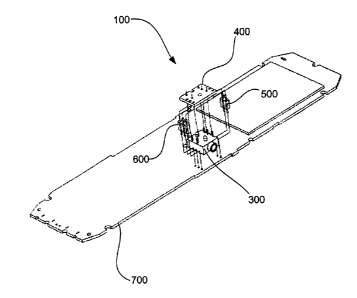
Figure 1 is schematic diagram showing an exploded state of
an exemplary system 100 for mounting electrical component
300 on printed circuit board (PCB) 700, while protecting the
electrical component 300 from mechanical stress and allowing
the electrical connections with PCB 700 to be redistributed,
in accordance with an embodiment of the present invention.
Electrical component 300 is mounted to carrier PCB 400 by
connecting the electrical component leads of electrical
component 300 to the component soldering pads of carrier PCB
400. Electrical component 300 is, therefore, connected
mechanically and electrically to carrier PCB 400 through the
electrical component leads of electrical component 300 and
the component soldering pads of carrier PCB 400. Carrier
PCB 400 redistributes one or more electrical signals
received from the electrical component leads through the
component soldering pads to the header connector soldering
pads of carrier PCB 400. This redistribution of electrical
signals effectively redistributes the electrical connections
of electrical component 300 on carrier PCB 400 and, in turn,
on PCB 700.
Header connector 500 and header connector 600 mechanically
connect carrier PCB 400 to PCB 700. The header connector
leads on one side of the header connector housing of header
connector 500 connect to the header connector soldering pads
of carrier PCB 400, and the header connector leads on the
other side of the header connector housing of header
CA 02531598 2005-12-23
g
connector 500 connect to PCB soldering pads 710 of PCB 700.
Likewise, the header connector leads on one side of the
header connector housing of header connector 600 connect to
the header connector soldering pads of carrier PCB 400, and
S the header connector leads on the other side of the header
connector housing of header connector 600 connect to the PCB
soldering pads of PCB 700. Header connector 500 and header
connector 600 connect carrier PCB 400 to PCB 700 so that
electrical component 300 is sandwiched between carrier PCB
400 and PCB 700. Header connector 500 and header connector
600 are located on opposite sides of electrical component
300 to provide the greatest amount of mechanical strength
and stability.
Header connector 500 and header connector 600 also
electrically connect carrier PCB 400 to PCB 700. Header
connector 500 and header connector 600 are used to carry at
least one electrical signal from a header connector
soldering pad of carrier PCB 400 to a soldering pad of PCB
700. In another embodiment of the present invention, header
connector 500 and header connector 600 are used to carry all
of the electrical signals from the header connector
soldering pads of carrier PCB 400 to the soldering pads of
PCB 700.
In order to provide the greatest possible mechanical
strength to system 600, the electrical component housing of
electrical component 300, is substantially in contact with
carrier PCB 400, PCB 700, the header connector housing of
header connector 500, and the header connector housing of
header connector 600. In alternative embodiments of the
present invention that provide less mechanical strength to
system 600, the electrical component housing of electrical
component 300, is not substantially in contact with carrier
PCB 400, PCB 700, the header connector housing of header
CA 02531598 2005-12-23
9
connector 500, or the header connector housing of header
connector 600.
In another embodiment of the present invention, guide pins
of the electrical component housing of electrical component
S 300 that protrude from the electrical component housing are
used to further secure electrical component 300 mechanically
to carrier PCB 400. The guide pins of the electrical
component housing of electrical component 300 are inserted
into carrier PCB holes of carrier PCB 400 when electrical
component 300 is mounted to carrier PCB 400.
In another embodiment of the present invention, second guide
pins (not shown) of the electrical component housing of
electrical component 300 that protrude from the electrical
component housing are used to further secure electrical
component 300 mechanically to PCB 700. These second guide
pins protrude from the electrical component housing 510 on
the side opposite to the guide pins that mechanically
connect electrical component 300 with carrier PCB 400.
These second guide pins can be formed into a shape including
but not limited to a substantially cylindrical, a
substantially rectangular shape, a substantially spherical
shape, a substantially triangular shape, or a tablet shape.
These second guide pins of the electrical component housing
of electrical component 300 are inserted into corresponding
holes (not shown) in PCB 700, when carrier PCB 400 is
mounted to PCB 700. These corresponding holes can be formed
into a shape including but not limited to a substantially
cylindrical, a substantially rectangular shape, a
substantially spherical shape, a substantially triangular
shape, or a tablet shape.
In another embodiment of the present invention, a third
header connector (not shown) mechanically connects carrier
PCB 400 to PCB 700 and is located on a third side of
CA 02531598 2005-12-23
electrical component 300. This third header connector can
also electrically connect a header connector soldering pad
of carrier PCB 400 with a PCB soldering pad of PCB 700. In
order to provide the greatest possible mechanical strength
5 to this embodiment, the housing of third header connector is
substantially in contact with the electrical component
housing of electrical component 300. In an alternative
embodiment, the housing of third header connector is not
substantially in contact with the electrical component
10 housing of electrical component 300 and provides less
mechanical strength.
Figure 2 is schematic diagram showing an assembled state of
an exemplary system 200 for mounting an electrical component
300 on a PCB 700, while protecting electrical component 300
from mechanical stress and allowing the electrical
connections with PCB 700 to be redistributed, in accordance
with an embodiment of the present invention. Electrical
component 300 is show in Figure 2 mounted to carrier PCB
400, sandwiched between carrier PCB 400 and PCB 700, and
secured on either side by header connector 500 and header
connector 600.
Figure 3 is schematic diagram showing an exemplary
electrical component 300, in accordance with an embodiment
of the present invention. Some electrical components are
subject to such significant impacts or so much repeated
mechanical stress that their housings and their soldering
joints can be damaged. These electrical components can
include, for example, switches, connectors, displays, fans,
transmitters, receivers, transformers, or LEDs. Electrical
component 300 is depicted in Figure 3 as a headset jack.
Electrical component housing 31 includes headset connector
port 320. One skilled in the art will appreciate that a
headset jack is a type of connector and is subject to
CA 02531598 2005-12-23
11
significant impacts or repeated mechanical stress during
normal plugging and unplugging operations performed by a
user.
Electrical component 300 is also depicted in Figure 3 as a
through-hole mounted component. Electrical component leads
330 are shown as through-hole type leads. One skilled in
the art will appreciate that a through-hole mounted
component provides greater mechanical strength than a
surface mounted component. The present invention, however,
is not limited to through-hole mounted components. In
another embodiment of the present invention, electrical
component 300 can be a surface mounted component with
surface mount leads.
Electrical component 300 includes alignment pins or guide
pins 340 of electrical component housing 310 that protrude
from electrical component housing 310. Guide pins 340 are
used to further secure electrical component 300 mechanically
to PCB 700, as illustrated in Figure 1 and Figure 2. Guide
pins 340 can be formed into a shape including but not
limited to a substantially cylindrical, a substantially
rectangular shape, a substantially spherical shape, a
substantially triangular shape, or a tablet shape.
Figure 4 is schematic diagram showing an exemplary carrier
PCB 400, in accordance with an embodiment of the present
invention. Carrier PCB 400 is configured to accept the
mounting of electrical component 300 (shown in Figure 1).
Component soldering pads 410 are designed to accept the
electrical component leads 330 of electrical component 300.
One skilled in the art will appreciate that component
soldering pads 410 are soldering via holes for a through-
hole mounted electrical component and surface mount
soldering pads for a surface mounted electrical component.
CA 02531598 2005-12-23
12
Carrier PCB holes 420 are configured to accept guide pins
340 of electrical component 300. Carrier PCB holes 420 are
formed into a shape including but not limited to a
substantially cylindrical, a substantially rectangular
shape, a substantially spherical shape, a substantially
triangular shape, or a tablet shape. Carrier PCB holes 420
in conjunction with guide pins 340 of electrical component
300 provide additional mechanical strength for the mounting
of electrical component 300 on carrier PCB 400.
Header connector soldering pads 430 are configured to accept
leads of header connectors, which, in turn, connect carrier
PCB 400 to a main PCB. One skilled in the art will
appreciate that header connector soldering pads 430 are
soldering via holes for through-hole mounted header
connector leads and surface mount soldering pads for surface
mounted header connector leads.
Carrier PCB 400 allows an electrical signal of electrical
component 300 to be physically relocated. Carrier PCB 400
relocates an electrical signal of electrical component 300
by connecting a component soldering pad 410 with a header
connector soldering pad 430. The electrical signal of an
electrical component lead 330 of electrical component 300
connected to a component soldering pad 410 is then
effectively relocated to a header connector mounted to a
header connector soldering pad 430. By allowing the
locations of header connector soldering pads 430 to be
moved, carrier PCB 400 provides a main PCB designer with a
greater amount of flexibility in placing the electrical
connections of electrical component 300 on the main PCB.
In another embodiment of the present invention, carrier PCB
400 allows all of the electrical signals of electrical
component 300 to be physically relocated. Carrier PCB 400
relocates all of the electrical signals of electrical
CA 02531598 2005-12-23
13
component 300 by connecting each of the component soldering
pads 410 with corresponding header connector soldering pads
430.
Figure 5 is schematic diagram showing an exemplary header
connector 500 with four header connector leads 510, in
accordance with an embodiment of the present invention.
Header connector leads 510 are enclosed in header connector
housing 520. Header connector 500 conducts electrical
signals from header connector leads 510 on one side of
header connector housing 520 to corresponding header
connector leads 510 on the other side of header connector
housing 520. Header connector leads 510 of header connector
500 are shown as through-hole leads. One skilled in the art
will appreciate that header connector leads 510 can include
through-hole leads or surface mount leads, although through-
hole leads provide greater mechanical strength. One skilled
in the art will further appreciate that header connector
leads 510 on one side of header connector housing 520 can be
through-hole leads and header connector leads 510 on the
other side of header connector housing 520 can be surface
mount leads.
A header connector can contain two or more header connector
leads. Figure 6 is schematic diagram showing an exemplary
header connector 600 with six header connector leads 610
enclosed by header connector housing 620, in accordance with
an embodiment of the present invention. One skilled in the
art will appreciate that the amount of mechanical strength
provided by a header connector is proportional to the number
of header connector leads 610.
Figure 7 is schematic diagram showing an exemplary PCB 700,
in accordance with an embodiment of the present invention.
PCB 700 is a main PCB and is designed to connect to carrier
PCB 400 (shown in Figure 4). PCB 700 includes PCB soldering
CA 02531598 2005-12-23
14
pads 710. PCB soldering pads 710 are designed to accept
header connector leads, which, in turn, connect carrier PCB
400 to PCB 700. One skilled in the art will appreciate that
PCB soldering pads 710 are soldering via holes for through-
hole mounted header connector leads and surface mount
soldering pads for surface mounted header connector leads.
Figure 8 is a flowchart showing a method 800 for mounting an
electrical component on a printed circuit board, while
protecting the electrical component from mechanical stress
and allowing the electrical connections with the printed
circuit board to be redistributed, in accordance with an
embodiment of the present invention.
In step 810 of method 800, an electrical component is
mounted on a carrier printed circuit board. At least one
electrical connection of the electrical component is
distributed from a lead of the electrical component to a
soldering pad of the carrier printed circuit board by the
carrier printed circuit board. The electrical component can
be a surface mounted component or a through-hole mounted
component. The electrical component can be but is not
limited to a switch, a connector, a fan, a display, a
transmitter, a receiver, a transformer, or an LED.
In step 820, a first header connector is connected to the
carrier printed circuit board on one side of the electrical
component.
In step 830, a second header connector is connected to the
carrier printed circuit board on the opposite side of the
electrical component.
In step 840, the first header connector is connected to the
printed circuit board. The first header connector
electrically connects the soldering pad of the carrier
printed circuit board with a soldering pad of the printed
circuit board.
CA 02531598 2005-12-23
In step 850, the second header connector is connected to the
printed circuit board. The carrier printed circuit board
and the printed circuit board are connected by the first
header connector and second header connector so that the
5 electrical component is located between the carrier printed
circuit board and the printed circuit board. In another
embodiment of this method, the second header connector
electrically connects the soldering pad of the carrier
printed circuit board with a soldering pad of the printed
10 circuit board.
In another embodiment of the present invention, a carrier
PCB, a first header connect and a second header connector
are used to mechanically secure a an electrical component to
a PCB. Connecting wires are used to electrically connect
15 the electrical component to the PCB. Figure 9 is schematic
diagram showing an exploded state of an exemplary system 900
for mounting an electrical component 300 on a PCB 700, while
protecting electrical component 300 from mechanical stress
and allowing the electrical connections with PCB 700 to be
redistributed using connecting wires 910, in accordance with
an embodiment of the present invention.
Electrical component 300 is mounted to carrier PCB 400 by
connecting the electrical component leads of electrical
component 300 to the component soldering pads of carrier PCB
400. Electrical component 300 is, therefore, connected
mechanically to carrier PCB 400 through the electrical
component leads of electrical component 300 and the
component soldering pads of carrier PCB 400.
Header connector 500 and header connector 600 mechanically
connect carrier PCB 400 to PCB 700. The header connector
leads on one side of the header connector housing of header
connector 500 connect to the header connector soldering pads
of carrier PCB 400, and the header connector leads on the
CA 02531598 2005-12-23
16
other side of the header connector housing of header
connector 500 connect to the PCB soldering pads of PCB 700.
Likewise, the header connector leads on one side of the
header connector housing of header connector 600 connect to
the header connector soldering pads of carrier PCB 400, and
the header connector leads on the other side of the header
connector housing of header connector 600 connect to the PCB
soldering pads of PCB 700. Header connector 500 and header
connector 600 connect carrier PCB 400 to PCB 700 so that
electrical component 300 is sandwiched between carrier PCB
400 and PCB 700. Header connector 500 and header connector
600 are located on opposite sides of electrical component
300 to provide the greatest amount of mechanical strength
and stability.
Electrical component 300 is connected electrically to PCB
700 using connecting wires 910. Connecting wires 910
electrically connect the leads of the electrical component
300 directly to soldering pads on PCB 700. Alternatively,
the electrical signals from the leads of electrical
component 300 are distributed by carrier PCB 400 to
soldering pads of carrier PCB 400, and connecting wires 910
electrically connect the soldering pads of carrier PCB 400
to the soldering pads on PCB 700.
Figure 10 is a schematic diagram showing an assembled state
of an exemplary system 1000 for mounting an electrical
component 300 on a PCB 700, where connecting wires 910
electrically connect the electrical leads of electrical
component 300 to PCB 700. In system 1000, connecting wires
910 carry the electrical signals from the electrical leads
of electrical component 300 directly to PCB 700.
Figure 11 is a schematic diagram showing an assembled state
of an exemplary system 1100 for mounting an electrical
component 300 on a PCB 700, where connecting wires 910
CA 02531598 2005-12-23
17
electrically connect carrier PCB 400 to PCB 700. In system
1100, the electrical signals from the leads of electrical
component 300 are distributed to soldering pads on carrier
PCB 400. Connecting wires 910 carry the electrical signals
S from the soldering pads of carrier PCB 400 to PCB 700.
Figure 12 is schematic diagram showing an exploded state of
an exemplary system 1200 for mechanically securing
electrical component 1230 mounted on PCB 1270, in accordance
with an embodiment of the present invention. In system
1200, electrical component 1230 is mounted to PCB 1270.
Electrical component 1230 is additionally mechanically
secured to PCB 1270 using PCB 1240, header connector 1250,
and header connector 1260. Header connector 1250 and header
connector 1260 are preferably mounted to PCB 1240. Header
connector 1250 and header connector 1260 are then preferably
mounted to PCB 1270 so that electrical component 1230 is
located between PCB 1270 and PCB 1240, and header connector
1250 and header connector 1260 are located on opposite sides
of electrical component 1230.
Figure 13 is schematic diagram showing an assembled state of
an exemplary system 1300 for mechanically securing
electrical component 1230 mounted on a PCB 1270, in
accordance with an embodiment of the present invention. In
system 1300, the housing of electrical component 1230 is
substantially in contact with PCB 1240 in order to provide
mechanical support. In other embodiments of the present
invention, the housing of electrical component 1230 is
substantially in contact with the housing of header
connector 1250, the housing of header connector 1260, or the
housing of header connector 1250 and the housing of header
connector 1260. One skilled in the art will appreciated
that system 1300 performs the function previously provided
by a custom made component strap. System 1300
CA 02531598 2005-12-23
Ig
advantageously performs the function of a custom made
component strap using standard soldering components.
Systems and methods in accordance with an embodiment of the
present invention disclosed herein can advantageously
protect an electrical component from mechanical stress and
distribute the electrical connections of the electrical
across a densely populated PCB. Connecting the electrical
component to a small PCB and sandwiching the component
between the small PCB and the densely populated PCB using
header connectors, protects the electrical component from
significant impacts or repeated mechanical and obviates the
need for a custom made plastic or metal bracket. Routing
the electrical connection of the electrical component from
the leads of the electrical component to the small PCB board
and then to the densely populated PCB, allows the designer
of the densely populated PCB more flexibility in placing the
electrical connections of the electrical component on the
densely populated PCB.
The foregoing disclosure of the preferred embodiments of the
present invention has been presented for purposes of
illustration and description. It is not intended to be
exhaustive or to limit the invention to the precise forms
disclosed. Many variations and modifications of the
embodiments described herein will be apparent to one of
ordinary skill in the art in light of the above disclosure.
The scope of the invention is to be defined only by the
claims appended hereto, and by their equivalents.
Further, in describing representative embodiments of the
present invention, the specification may have presented the
method and/or process of the present invention as a
particular sequence of steps. However, to the extent that
the method or process does not rely on the particular order
of steps set forth herein, the method or process should not
CA 02531598 2005-12-23
19
be limited to the particular sequence of steps described.
As one of ordinary skill in the art would appreciate, other
sequences of steps may be possible. Therefore, the
particular order of the steps set forth in the specification
should not be construed as limitations on the claims. In
addition, the claims directed to the method and/or process
of the present invention should not be limited to the
performance of their steps in the order written, and one
skilled in the art can readily appreciate that the sequences
may be varied and still remain within the spirit and scope
of the present invention.