Note: Descriptions are shown in the official language in which they were submitted.
CA 02531783 2006-O1-06
WO 2005/008578 PCT/US2004/021951
RFID DEVICE WITH CHANGEABLE CHARACTERISTICS
BACKGROUND OF THE INVENTION
FIELD OF THE INVENTION
[0001] This invention relates to the field of radio frequency identification
(RFID) tag
and label detection systems, and to methods of detecting RFID tags and labels.
DESCRIPTION OF THE RELATED ART
[0002] Radio frequency identification (RFID) tags and labels (collectively
referred to
herein as "devices") are widely used to associate an object with an
identification
code. RFID devices generally have a combination of antennas and analog and/or
digital electronics, which may include for example communications electronics,
data
memory, and control logic. For example, RFID tags are used in conjunction with
security-locks in cars, for access control to buildings, and for tracking
inventory and
parcels. Some examples of RFID tags and labels appear in U.S. Patent Nos.
6,107,920, 6,206,292, and 6,262,292, all of which are hereby incorporated by
reference in their entireties.
[0003] As noted above, RFID devices are generally categorized as labels or
tags.
RFID labels are RFID devices that are adhesively or otherwise have a surface
that is
attached directly to objects. RFID tags, in contrast, are secured to objects
by other
means, for example by use of a plastic fastener, string or other fastening
means.
Nevertheless, RFID devices are referred to herein somewhat interchangeably as
"tags" or "labels."
[0004] RFID devices include active tags and labels, which include a power
source,
and passive tags and labels, which do not. In the case of passive tags, in
order to
retrieve the information from the chip, a "base station" or "reader" sends an
excitation
signal to the RFID tag or label. The excitation signal energizes the tag or
label, and
the RFID circuitry transmits the stored information back to the reader. The
"reader"
receives and decodes the information from the RFID tag. In general, RFID tags
can
retain and transmit enough information to uniquely identify individuals,
packages,
inventory and the like. RFID tags and labels also can be characterized as to
those to
which information is written only once (although the information may be read
repeatedly), and those to which information may be written during use. For
example,
CA 02531783 2006-O1-06
WO 2005/008578 PCT/US2004/021951
RFID devices may store environmental data (that may be detected by an
associated
sensor), logistical histories, state data, etc.
[0005] In activating, reading, and/or detecting RFID devices, radio frequency
(RF)
fields are generally sent over a relatively long range, that is, over
intervening free
space. Thus detection of devices is accomplished over a significantly-sized
region,
and spatial discrimination in reading and detection of devices may be
difficult.
[0006] ~ne concern that has been raised regarding RFID devices is that their
ability
to be read over relatively long distances may implicate privacy concerns for
people
having objects with RFID devices attached thereto or otherwise coupled
thereto.
[0007] In addition, RFID devices may include commercially-sensitive
information
that is utilized in channels of commerce in supplying products to an end user.
It may
be desirable that this information rendered ungatherable or more difficult to
gather
after the product reaches the end user.
[000] It will be appreciated that concerns about possible tracking or other
privacy-
related issues, or issues involving undesired dissemination of commercially-
sensitive
information, may inhibit some users from employing RFID devices. Accordingly,
it
will be appreciated that it would be desirable for RFID devices to avoid the
above
problems.
SUMMARY ~F THE INVENTI~N
[0009] According to an aspect of the invention, an RFID includes at least a
portion
that has alterable characteristics.
[0010] According to another aspect of the invention, an RFID device has a
first
portion and an inactivatable second portion. The device may be read at a
greater
range when the second portion is not inactivated, than when the second portion
is
inactivated.
[0011] According to yet another aspect of the invention, an RFID device
includes a
first portion and an inactivatable second portion, wherein the inactivatable
second
portion includes an antenna. Even with the second portion inactivated, the
RFID
device may be read at short range.
[0012] According to a further aspect of the invention, an RFID device has a
first
portion and an inactivatable second portion, wherein the second portion may be
inactivated by contact with a suitable solvent. The solvent may be a
substance, such
2
CA 02531783 2006-O1-06
WO 2005/008578 PCT/US2004/021951
as water, that dissolves at least part of the inactivatable second portion,
such as a
substrate, and/or a material placed upon the substrate.
[0013] According to a still further aspect of the invention, an RFID device
includes
an inactivatable portion that is inactivated by contact with a suitable
material having
pre-determined characteristics. For example, the second portion may be
inactivatable by exposure to water above a certain temperature, while not
being
inactivated by exposure to water below the given temperature. As another
example,
the inactivatable portion may be inactivated by exposure to water having an
additive,
such as a detergent, while not being inactivated by exposure to water without
the
additive.
[0014] According to another aspect of the invention, an RFID device includes a
first
portion and an inactivatable second portion, wherein the first portion is
sealed to
prevent contact with a solvent, abrasion, or other contaminants and/or
potentially
damage-producing situations.
[0015] According to another aspect of the invention, an RFID device is
configured
so as to change characteristics upon laundering of an object, such as a
garment, to
which the RFID device is attached or otherwise coupled.
[0016] According to a still further aspect of the invention, an RFID device
includes a
first portion and an inactivatable second portion, wherein the inacfiivatable
second
portion may be physically separated from the first portion along a
predetermined
boundary.
[0017] According to a further aspect of the invention, an RFID device includes
a
first portion and an inactivatable second portion wherein the second portion
is
inactivated by normal use of an object to which the RFID device is coupled.
[001 ~] According to a still further aspect of the invention, a radio
frequency
identification (RFID) device includes a first portion and a second portion
operatively
coupled to the first portion. The second portion is alterable upon occurrence
of a
predetermined event. The device has different electrical characteristics
depending
on whether the second portion is altered.
[0019] According to another aspect of the invention, a method of associating
information with an object includes: coupling an RFID device to the object,
wherein
the RFID device is configured to change electrical characteristics during
expected
use of the object; and transferring the object to a user.
3
CA 02531783 2006-O1-06
WO 2005/008578 PCT/US2004/021951
(0020] According to yet another aspect of the invention, a method of at least
reducing accessibility of information associated with an object includes
receiving an
object with an RFID device coupled thereto, wherein the RFID device is
configured
to have read characteristics of the RFID device changed by occurrence of a
predetermined event associated with ordinary use of the object; and changing
read
characteristics of the device by using the object in an ordinary way.
[0021] According to still another aspect of the invention, a radio frequency
identification (RFID) device including a transponder chip; and an antenna
coupled to
the chip. Coupling between the chip and at least part of the antenna is
alterable
upon occurrence of a predetermined event. The device has different electrical
characteristics depending on whether the coupling between the chip and the at
least
part of the antenna is altered.
[0022] To the accomplishment of the foregoing and related ends, the invention
comprises the features hereinafter fully described and particularly pointed
out in the
claims. The following description and the annexed drawings set forth in detail
certain
illustrative embodiments of the invention. These embodiments are indicative,
however, of but a few of the various ways in which the principles of the
invention
may be employed. ~ther objects, advantages and novel features of the invention
will become apparent from the following detailed description of the invention
when
considered in conjunction with the drawings.
ERIEF DESCRIPTI~N ~F THE DRAWINGS
(0023] In the annexed drawings, which are not necessarily according to scale:
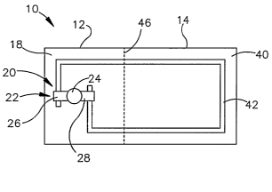
(0024] Fig. 1 is a plan view of an RFID device in accordance with the present
invention;
[0025] Fig. 2 is a cross-sectional side view of a prior art interposer or
strap that may
be part of the device of Fig. 1;
(0026] Fig. 3 illustrates the RFID device of Fig. 1 incorporated into a
garment;
[0027] Fig. 4 is a plan view of one embodiment of the device of Fig. 1, a
device with
a soluble substrate;
[0028] Fig. 5 is a plan view of another embodiment of the device of Fig. 1, a
device
with a soluble portion of an antenna;
4
CA 02531783 2006-O1-06
WO 2005/008578 PCT/US2004/021951
[0029] Fig. 6 is a plan view of yet another embodiment of the device of Fig.
1, a
device with one or more soluble antenna links;
[0030] Fig. 7, is a plan view of an embodiment of the device of Fig. 1 that
include a
sealing material;
[0031] Fig. 8 is a plan view of an embodiment of the device of Fig. 1 that is
configured to be severed;
[0032] Fig. 9A shows the device of Fig. 8 attached to a container;
[0033] Fig. 9S shows another example of the device of Fig. 8 attached to a
container;
[0034] Figs. 10-12 are views of various objects with RFID devices of the
present
invention coupled thereto, to be subjected to various physical forces during
use of
the objects;
[0035] Fig. 13A is a plan view illustrating an RFID device of the present
invention
with a protective coating applied to a portion thereof;
[0036] Fig. 13S is a plan view of a portion of an RFID device of the present
invention that has electrical characteristics that are altered upon stretching
of the
device;
[0037] Fig. 14 is a schematic illustration showing electrical coupling between
an
RFID device of the present invention, and an object having a circuit;
[003] Fig. 15 is a plan view of an RFID device in accordance with the present
invention, having fusible electrical connections;
[0039] Fig. 16 is a schemafiic illustration of the device of Fig. 15,
incorporated into a
computer;
[0040] Fig. 17 is a plan view of an RFID device in accordance with the present
invention, having an alterable RFID chip;
[0041] Fig. 18 is a schematic illustration of an RFID device having an
alterable
RFID chip, incorporated into a mobile telephone;
[0042] Fig. 19 is a view of an RFID device in accordance with the present
invention,
incorporated in a battery-operated device; and
[0043] Fig. 20 is a view of a semi-passive RFID device in accordance with the
present invention, having alterable characteristics.
DETAILED DESCRIPTION
CA 02531783 2006-O1-06
WO 2005/008578 PCT/US2004/021951
[0044] An RFID device includes a first, relatively permanent portion and a
second
alterable or inactivatable portion. Upon the occurrence of some predetermined
event, the second portion and/or its coupling to the first portion is
physically altered,
inactivating it. The first portion may itself be an antennaless RFID device
that may
be read at short range, and the second portion may be an antenna that, when
coupled to the first portion, substantially increases the range at which the
first portion
may be read. The second portion may be configured to be altered or inactivated
by
any of a variety of tasks performed either on the RFID device, or upon an
object to
which the RFID device is coupled. Examples of ways in which the second portion
may be inactivated include exposure to a suitable solvent, such as water used
in a
laundering process; tearing or otherwise physically separating the second
portion
from the first portion; other applications of physical force that may be part
of regular
use of the object to which the RFID device is coupled; and application of
electrical
forces.
[0045] In further explanation of a broad overview of the invention, an RFID
device
may include an electronic circuit such as an integrated circuit (also referred
to herein
as a chip), an antenna having one or more antenna elements, and an electrical
coupling or connection between the electronic circuit and the antenna. The
RFID
device includes an alterable portion that alfiers or disables function of the
RFID
device upon occurrence of some predetermined event. A "predetermined event",
as
the term is used herein, is defined as some event that is likely to occur in
normal
transfer or use of an object to which the RFID device is coupled, but is not
likely to
occur prior to such normal transfer and use. A predetermined event may be a
physical, chemical, or electrical event. The alterable portion may be a
soluble
portion, for instance a soluble antenna portion, that is dissolved in the
presence of
some solvent, for example in water or a water and detergent combination. The
alterable portion may be a portion of the electrical coupling that changes
composition
(and thus its electrical coupling characteristics) when exposed to a suitable
reactant.
The alterable portion may be a portion of the coupling or antenna that alters
or
changes electrical characteristics (such as by narrowing or breaking) when
subjected
to a tensile force or an impact force. The alterable portion may include a
portion that
is severed or physically separated from the rest of the RFID device. The
alterable
portion that may include a portion that is configured to be altered in
function by a
6
CA 02531783 2006-O1-06
WO 2005/008578 PCT/US2004/021951
suitable electrical event, such as by powering up of an electrical or
electronic device
which the RFID device is coupled to or which the RFID device is a part of. The
electrical event may, for example, alter or disconnect portions of the antenna
of the
RFID device, or may disable or alter function of the chip of the RFID device.
[0046] Alteration of the alterable portion may cause the RFID device to become
fully non-functional (non-readable or non-detectable). Alternatively,
alteration of the
alterable portion may cause the RFID device to continue functioning, but with
altered
characteristics. For instance, the altered characteristics may include a
reduction in
the distance at which the RFID device may be read or detected. This may be
done
by decoupling the RFID chip from the antenna, or by reducing the amount of the
antenna that is effectively coupled to the RFID chip. Even when the RFID chip
is
decoupled from the antenna, the RFID chip may remain coupled to an interposer
or
strap, which may allow short-range detection of the RFID device.
[0047] The relatively-permanent portion of the RFID device may include an
antennaless device, which may be read by a proximity detector. As used herein,
the
term "antennaless" refers broadly to devices lacking an antenna that is viable
for
receiving RF energy for remote, long-range reading. In characterizing
antennaless
devices, it is useful to compare them with well-known antennaed structures. An
example of a well-known antenna structure is a dipole antenna with a good
impedance match between the antenna and an RFID chip. A good impedance
match provides good power transfer between antenna and chip. A dipole antenna
has an anfienna gain, relative to a perfect antenna, of approximately 2 dSi
(decibels
relative to an isotropic radiator- something that radiates equally in all
directions). In
a perfectly-impedance-matched situation, all of the power received by the
antenna
will be transmitted to the RFID chip.
[0048] Relative to structures described above having a perfect antenna or an
impedance-matched dipole antenna, an "antennaless" structure will perform
poorly.
Such poor performance may in part be due to an inherently low antenna gain
(due to
small physical dimensions of the structure relative to wavelengths of RF
energy).
Another factor in poor performance of antennaless structures may be a poor
impedance match between the chip and connected conductors (such as conductive
leads), which manifests itself as a further power loss. Thus in an antennaless
RFID
device there may be losses, relative to an RFID device, due to small size of
7
CA 02531783 2006-O1-06
WO 2005/008578 PCT/US2004/021951
conductive structures that could receive RF energy, and/or due to poor
impedance
match, limiting efficiency of power transfer between the conductive structures
and a
chip of the device.
[0049] An antennaless RFID device, as the term is used herein, is defined as a
device having a structure such that when it is placed in the far field of a
transmitter
(defined below), an RFID chip of the device that is attached to the structure
will
absorb -20d~ in power compared to an impedance-matched dipole antenna. Put in
other words, the structure of an antennaless device, when placed in the far
field of
an RF transmitter, provides to an attached RFID chip 1 % or less of the power
that an
impedance-matched dipole antenna would provide to the RFID chip.
[0050] An antennaless RFID device may be powered through use of a proximity
locator, a device that generates a short-range RF field, with relatively low
far-field RF
radiation. The far field, as used herein, refers to a distance greater than
about 15
mm from an RF-energy emitting device, such as device that emits UHF RF energy.
Coupling of an RFID device in fihe far field is also referred to as "long-
range
coupling." The near field, where short-range coupling may occur, is defined as
less
than approximately 15 mm from an RF-energy emitting device. Placement of the
RFID device in the near field is also referred to herein as placement of the
device in
"close proximity" to the proximity locator or parts of the proximity locator.
[0051] An example of UHF RF energy, referred to above, is RF energy in the
range
of 060 MHz to 950 IUiHz. However, it will be understood that a wide variety of
other
RF frequencies may be utilized, including frequencies other than UHF RF
frequencies. For instance, frequencies of about 2-3 GHz may be utilized,
although it
will be appreciated that the short-range-coupling outer range limit from the
RF-
energy emitting device may be reduced when higher frequencies are employed.
[0052] A proximity detector of locator for detecting the presence of antennaed
or
antennaless RFID devices may include two or more conductors that create a
suitable
electrical field between the conductors or in the vicinity of the conductors.
The
conductors may be capacitively coupled to the RFID device to provide power to
the
RFID device, or to otherwise interact with the RFID device, allowing detection
of
devices in the vicinity of the electrical field.
CA 02531783 2006-O1-06
WO 2005/008578 PCT/US2004/021951
[0053] Further information regarding proximity devices or locators may be
found in
commonly-owned U.S. Application No. 10/406,702, which is herein incorporated
by
reference in its entirety.
[0054] Referring initially to Fig. 1, an RFID device 10 with changeable
characteristics is shown. The RFID device 10 has a first portion 12 with
relatively
permanent read characteristics, and a second portion 14, which is
inactivatable or
otherwise changes characteristics.
[0055] The first portion 12 includes a first portion substrate 18 with an
antennaless
device 20 such as a strap or interposes 22 thereupon. The interposes or strap
22
includes a chip 24 (also referred to as a microchip) connected to conductive
leads 26
and 28.
[0056] With reference now to Fig. 2, details of the interposes or strap 22 are
now
described further. As stated above, the interposes or strap 22 includes the
chip 24
and the conductive leads 26 and 28. The leads 26 and 28 operatively coupled to
chip contacts 30 of the chip 24. The chip 24 may be referred to herein in
addition as
an "electronic element." The chip 24 may include any of a variety of suitable
electronic components, such as the circuitry described above for modulating
the
impedance of the RFID device 10.
[0057] The leads 26 and 28 may be completely made out of an electrically
conducting material, such as being made out of a metal foil. Alternatively,
the leads
26 and 28 may include an electrically insulating material, for example being
plastic
coated with metal. The interposes or strap 22 may include an interposes
substrate
34 that is attached to the leads 26 and 28. The interposes substrate 34 may be
made of any of a variety of suitable materials, for example, suitable flexible
polymeric
materials such as PET, polypropylene or other polyolefins, polycarbonate, or
polysulfone. Alternatively or in addition, the interposes substrate 34 may
include a
conductive material, such as a metal or a metal foil.
[0058] The interposes or strap 22 may be any of a variety of commercially-
available
interposers or straps. Examples include an RFID interposes or strap available
from
Alien Technologies, and the interposes or strap marketed under the name (-
CONNECT, available from Philips Electronics. Alternatively, the interposes or
strap
22 may be other than a commercially-available interposes or strap.
9
CA 02531783 2006-O1-06
WO 2005/008578 PCT/US2004/021951
[0059] The leads 26 and 23 may have a length of approximately 7 mm. An
antennaless RFID device with leads 7 mm long would be suitable for receiving
RF
energy at very high frequencies, on the order of 20 GHz, but would not be
considered an antenna within the definition used herein.
[0060] More broadly, the leads may have a length of up to one-tenth of a
wavelength at the operating frequency, although, as stated earlier it is
desirable to
minimize this for cost reasons. For example, a wavelength of 327.3 mm
corresponds to an operating frequency of 915 MHz. Leads for such an operating
frequency may have a length up to 33 mm.
[0061] It will be understood that the terms "interposer" and "strap" are not
restricted
to the embodiment just described. The terms "interposer" and "strap," as used
herein, refer broadly to devices that include a microchip or other electronic
circuitry,
coupled to conductive leads. The conductive leads may be connected to contacts
on
the microchip or other circuitry by any of a variety of suitable methods.
[0062] The second portion 14 includes a second portion substrate 40 upon which
an antenna or portion of an antenna 42 is located. The antenna 42 is coupled
to the
antennaless device 20 that is part of the first portion 12. The antenna 42
then
coupled to the antennaless device 20, enables detection of the RFID device 10
as
longer ranges, relative to the detection of the antennaless device 20 alone.
[0063] The second portion 14 may be inactivatable, or otherwise changed in
operating characteristics, upon occurrence of one or more predetermined
events.
The event may involve physical separation of the second portion 14 from the
first
portion 12, such as by tearing, cutting, or severing along a boundary 46
between the
first portion 12 and the second portion 14. Alternatively, as explained in
greater
detail below, a physical, electrical, or chemical process may be utilized to
inactivate
or otherwise change characteristics to the second portion 14. Examples of
various
ways in which the second portion 14 may be inactivated or otherwise changed
are
described below.
[0064] The second portion 14 is described above as including the antenna 42.
It
will be appreciated that the inactivatable portion may be other than an
antenna. For
example, the inactivatable portion may be only part of an antenna, changing
the
range or other characteristics of the RFID device. The inactivatable portion
may be
one or components of the RFID device, such that the operating frequency of the
CA 02531783 2006-O1-06
WO 2005/008578 PCT/US2004/021951
RFID device is altered by inactivation of the inactivatable portion of the
device. For
instance, inactivation of the inactivatable portion of the device may cause
the device
operating frequency to change, say from 915 MHz to 2450 MHz.
[0065] It will be appreciated that a wide variety of alternatives may be made
in the
configuration of the RFID device 10. For example, the RFID device 10 may have
any of a variety of suitable antenna arrangements, and may have a wide variety
of
other suitable structures and/or configurations.
(0066] As another alternative, the RFID device 10 may be configured so that
remote readability of the device is totally destroyed by inactivation of the
inactivatable portion, such as the second portion 14. Such a device, when
inactivated, may be detectible and/or readable only by contact methods, i.e.,
by
methods involving actual physical contact with the chip 24.
[0067] Referring to Fig. 3, the RFID device 10 may be coupled to a washable
item,
such as a piece of clothing 50, for example, being on or within a label 52 of
the
article of clothing 50. For example, the label 52 may be a thermally
transferable
label. The second portion 14 of the device 10 may be configured so as to be
inactivated when the article of clothing 50 is laundered.
[0065] As one example of such a device, illustrated in Fig. 4, the second
portion
substrate 40 may include a soluble material 60 that dissolves when exposed to
a
suitable solvent. For example, the soluble substrate 60 may be a water-soluble
material, such as rice paper or another suitable material, that dissolves or
otherwise
breaks down when exposed to water. When the washable item 50 is laundered or
otherwise exposed to water, the soluble substrate 60 would break down, thereby
destroying the integrity of the second portion 14, and causing the antenna 42
to
separate. However, at least part of the first portion 12, such as the part
including the
antennaless device 20, may be configured to remain active, and readable
through
use of a proximity locator or detector, as described above.
[0069] The label 52 may include other layers, such as a printable layer
displaying
text and/or graphics. Soluble layers such as the soluble substrate 60 may be
laminated to the printable layer in such a way so that the text and/or
graphics are
viewable even after the soluble substrate 60 has been dissolved.
[0070] Another alternative is shown in Fig. 5, wherein the antenna 42 includes
at
least a portion 61 that is made of a soluble conductive material that is
soluble in
11
CA 02531783 2006-O1-06
WO 2005/008578 PCT/US2004/021951
water or another suitable solvent. Examples of suitable soluble conductive
materials
include soluble inks, such as those described in U.S. Patent Nos. 5,286,415
and
5,855,820, both of which are herein incorporated by reference in their
entireties. The
antenna 42 may be formed by printing conductive ink on the substrate 40 of the
second portion 14.
(007°1] In a specific embodiment, illustrated in Fig. 6, the antenna
portion 61 may be
one or more soluble conductive links 62. Removal of the soluble conductive
links 62
may deactivate the antenna 42 or decouple the antenna 42 from the first
portion 12.
Alternatively, the soluble conductive link 62 may be suitably located so as to
merely
alter the electrical characteristics of the antenna 42.
[0072] The first portion substrate 18 and the second portion substrate 40 may
include suitable materials, for example, suitable flexible polymeric
materials, such as
those described above for the substrate 34 of the strap 22 (Fig. 2).
[0073] For the embodiment shown in Fig. 4, the first portion substrate 18 may
be of
a different material from that of the second portion substrate 40.
Alternatively, or in
addition, with reference to Fig. 7, a sealing material 64 may be used to seal
all or
part of the first portion 12 to protect the interposer or strap 22, for
example, from
exposure to the water or other solvent that is used to deactivate the second
portion
14. The sealing material 64 may be a suitable epoxy or adhesive material.
[0074] It will be appreciated that the RFID device 10 that may be partially
inactivated by washing could be used advantageously in a variety of situations
in a
garment. For example, the fully-operational RFID device 10, with the active
second
portion 14, may be used to track the garment 50, prior to sale, at relatively
long
range, such as in a far-field region. For example, long-range detection may be
desirable in terms of inventory control tracking, facilitating gathering
information for
streamlining purchasing operations, and/or for theft prevention. Having the
second
portion 14 deteriorate during laundering may make the RFID device 10 less
intrusive,
for example, by reducing size and/or stiffness of the device, thereby
improving
comfort of the user of the garment 50. In addition, removing or changing the
long-
range detectability of the RFID device 10 may be advantageous to aid in
maintaining
privacy of the wearer or user of the garment 50. Still, it may be desirable to
have
means of short-range tracking of the RFID device 10, even when the second
portion
14 has been inactivated. Such short-range detection of the RFID device 10 may
aid
12
CA 02531783 2006-O1-06
WO 2005/008578 PCT/US2004/021951
in authenticating the garment 50, for example, in processing returns of the
garment.
For instance, a proximity locator or detector may be used to read information
from
the antennaless device 20 in a near-field region, to confirm that the garment
50 is
being returned to the same store from which it was purchased.
(0075] Another alternative is for the device 10 to be configured so as to
deteriorate
substantially completely upon occurrence of a predetermined event. For
example,
the entire substrate of the device may be made of a water-soluble material,
such as
rice paper. Some small portion of the device, such as an interposer or strap,
may
remain after the predetermined event, such as laundering of a garment to which
the
RFID device 10 is coupled. Configuration of the device so that substantially
the
entire substrate of the device is made of a water-soluble material is a
particularly
advantageous version in regard to the advantage noted earlier, i.e. reducing
the size
and/or stiffness of the device in order to improve the comfort of the user of
a garment
carrying the device.
[0076] It will be appreciated that many variations are possible in terms of
materials
and/or solvents utilized. For example, the second portion substrate 40 and/or
the
material of the antenna 42 or other structures in the second portion 14, may
be
configured to inactivate or otherwise change characteristics in response to
contact to
a material other than water. For example, the second portion 14 may be
configured
to become inactive in response to contact with materials used in dry cleaning
procedures, such as carbon tetrachloride. Alternatively, the second portion 14
may
be configured to be inactivatable by exposure to water of a certain minimum
temperature or to water containing a suitable detergent. It will be
appreciated that
such a feature may be utilized to reduce the probability of undesirable,
accidental or
deliberate inactivation of the long-range readability of the RFID device 10,
or as a
way of confirming that proper laundering of the garment 50 has taken place.
For
example, garments for use in a hospital may be configured to become partially
or
totally inactive only when washed in a minimum temperature of water. Long-
range
detection of laundered garments may be used to identify garments that have not
been properly laundered, due to such garments retaining such long-range
readability
of RFID devices.
[0077] Water solubility of water-soluble material may be changed by changing
the
molecular weight of a polymer utilized in a soluble ink, for example by
controlling
13
CA 02531783 2006-O1-06
WO 2005/008578 PCT/US2004/021951
crosslinking of the polymer. By increasing crosslinking of the polymer by a
suitable
amount, such as by a several-fold increase in molecular weight, the water-
soluble
material may become substantially insoluble in cold water, but still may
remain
soluble in hot water. The aforementioned U.S. Patent Nos. 5,286,415 and
5,855,820
disclose methods to graft water-soluble and water-insoluble hydrophobic
polymer.
Water solubility can be controlled by the amount of hydrophobic polymer in the
resultant graft copolymers.
[0078] Another alternative is a second portion 14 that includes a conductive
material that has its conductivity characteristics altered by exposure to a
predetermined substance or chemical, thereby changing the read characteristics
of
the RFID device. For example, the second portion 14 may have an antenna 42 may
of different conductive materials, one of which is water-soluble (hydrophilic)
and the
other of which is insoluble, either by being a hydrophobic material or being
coated to
prevent contact with water. The water-soluble material may be on top of the
insoluble material, so that exposure to water reduces the thickness of the
antenna
42. Alternatively, the water-soluble material may be adjoining and in contact
with the
insoluble conducfiive material, so that exposure to water decreases the width
of the
antenna 42. It will be appreciated that a variety of other configurations may
be
obtained that give the antenna 42 changed electrical characteristics upon
occurrence
of a triggering event.
[007] As another alternative, the RFID device 10 may include a portion that is
dissolved by exposure to a chemical composition that is mixed and activated
during
use of the product. For example, the RFID device 10 may be placed on a barrier
that is ruptured during activation of a device, such as a fluorescent device.
[0080] It will be appreciated that it may be possible to configure the RFID
device 10
so that such changes in characteristics are reversible, so as to make the RFID
device 10 re-usable as a detector of exposure to the chemical or substance.
For
example, exposure to a first substance could alter characteristics from a
first state to
a second, different state, while exposure to a second substance could alter
the
characteristics of the device back to the first state.
[0081] Many alternatives are possible for the location of a soluble substrate
or
substrate portion, or a soluble conductive link. For example, soluble
conductive
material may be used for a conductive link between the interposer or strap 22
and
14
CA 02531783 2006-O1-06
WO 2005/008578 PCT/US2004/021951
the rest of the RFID device 10. Removal of such soluble material may thereby
electrically isolate the interposer or strap 22. As another alternative, a
soluble
adhesive may be used to physically couple the interposer or strap 22 to the
rest of
the RFID device 10. Dissolution of the adhesive may physically separate the
interposer or strap 22 from the RFID device 10.
[0082] The RFID device 10 may include soluble structures other than antennas,
removal of which (by contact with a suitable solvent) may change the operating
characteristics of the RFID device 10. For example, a soluble adhesive may
used to
attach one part of the device 10 (such as an interposer or strap) to another
part
(such as the substrate with the conductive pattern (antenna) thereupon.
[0083] It will be appreciated that the RFID device 10 with a soluble portion
or
portions may be utilized in a wide variety of applications where an object is
washed
as part of its normal use, or otherwise comes into contact with a suitable
solvent.
[0084] Fig. 8 shows an RFID device 10 with a physically-separable second
portion
14, which may be inactivated by physically separating it from the first
portion 12
along a severing line 68. The severing may be any of a variety of physically
separating processes, such as cutting or tearing. The severing line 68 may be
an
area that is perforated, scored, or otherwise configured to make the severing
easier,
andlor to encourage severing at the desired location along the severing line
68.
[0085] Alternatively or in addition, the severing line 68 may correspond to a
visual
indicator such as a printed line, to aid in locating the severing in a proper
place. In
addition, the RFID device 10 may have instructions thereupon, in words andlor
symbols, directing an end user or other person to sever the RFID device 10
along
the severing line 68, to physically separate the second portion 14 from the
first
portion 12. For example, the RFID device 10 may have instructions such as "CUT
HERE" written thereupon, indicating to the user the severing line 68 where the
second portion 14 is to be separated from the first portion.
[0086] The severing line 68 is shown in Fig. 8 as a straight line. However, it
will be
appreciated that the severing line 68 may more broadly be a boundary of any
shape.
[0087] Fig. 9A shows the RFID device 10 of Fig. 8 mounted on an item 70 that
has
an opening seam 74, with the severing line 68 along the opening seam 74. The
RFID device 10 is severed along the severing line 68, thereby inactivating the
second portion 14, by opening of the item 70 along the opening seam 74. Thus,
the
CA 02531783 2006-O1-06
WO 2005/008578 PCT/US2004/021951
item 70 may be a box or other container configured such that in order to
conventionally open the container to access the inner contents, requires
inactivating
the second portion 14 of the RFID device 10 thereupon. A consumer then may be
required to cut, tear, or otherwise sever the RFID device, for example,
incapacitating
long-range readability of the RFID device, in order to open the container.
[0088] The item 70 may be a box or a folder that contains an object or objects
inside. Alternatively, the item 70 may be an object that includes a hinged or
other
openable portion, such as with a compact disk player with an opening for
receiving a
compact disk, or a hinged portable telephone that must be opened for
operation.
[0089] Fig. 9B shows an alternative mounting for the RFID device 10 of Fig. 8,
on a
container 76 that has a removable top 78. The container 76 may be a container
that
has a screw-off or pull-off top 78, such as a container for holding perfume or
medicines. The RFID device 10 may be adhered to the container 76 with parts of
the device 10 adhered to the top 78 and a body 79 of the container 76, with
the
device 10 configured relative to the container 76 such that the severing line
68 of the
device 10 is about at the location where the top 78 meets the body 79. When
the
container 76 is opened by separating the top 78 from fibs body 79, the RFID
device
is severed, altering characteristics of the RFID device 10. For instance, the
distance over which the RFID device 10 may be read may be reduced by the
severing. Thus, once the product is used by opening the container 76, the RFID
device 10 may be partially or fully reduced in function, protecting privacy of
a
consumer or end user.
[0090] In addition, the RFID device 10 shown in Figs. 9A and 9B may be
employed
as an anti-tampering device. The location of the RFID device 10 may prevent
opening of the item 70 or the container 76 without altering operation of the
RFID
device 10. Thus tampering prior to sale of the item 70 or the container 76 may
be
detectable by an RFID reader mounted in a display unit, such as a shelf, or at
a point
of sale location, such as a cash register. In addition, severing of the RFID
device 10
may be detected visually, by either a retailer or a consumer. Thus tampering
with
products may be discouraged by making such tampering easily detectable.
[0091] Figs. 10-12 illustrate those situations where the RFID device is placed
on an
object and is thereby subjected to various types of physical forces
encountered in
ordinary use of the object. Fig 10 shows the RFID device 10 on an object 80,
such
16
CA 02531783 2006-O1-06
WO 2005/008578 PCT/US2004/021951
as a compact disk or a centrifuge, that may be subjected to centrifugal forces
32 in
ordinary use. Fig. 11 shows the RFID device 10 on or as part of an object 90
that is
subjected to stretching forces 92 during use. An example of an object 90 is a
vehicle
tire that is stretched during installation on a vehicle wheel. Fig. 12 shows
an RFID
device on an object, such as the sole of a shoe 100, that is subjected to
abrasive or
other wearing forces during regular use. In all of these configurations shown
in Figs.
10-12, the RFID device 10 may be configured such that the second portion 14 is
subject to change by the physical forces encountered in use of the objects 30,
90,
and 100, while the first portion 12 is less affected or unaffected by the
various
physical forces.
[0092] Wifih regard to Fig. 13A, the device 10 may have a strengthening
coating
110 over at least part of the first portion 12, to provide strength or
otherwise aid in
protecting at least part of the first portion 12 from damage or other
alterations due to
physical force.
[0093] Fig. 13~ shows a portion 111 of an RFID device 10 that has electrical
characteristics that are alterable by stretching. The portion 110 has a
substrate 112
with a conductive trace 114 thereupon. The conductive trace 114 may be a part
of
an antenna or other electrical connection. The substrate 112 may be any of a
variety
of suifiable materials that could support a conductive trace, such as a
conductive ink
trace, and would be sufficiently stretchable to allow alteration of the
electrical
characteristics of the conductive trace. ~ne broad category of suitable
substrate
materials is unoriented polyolefins, for example having a thickness from about
25
and 200 pm (microns). Another example of a suitable material for the substrate
114
is a suitable paper layer. The conductive trace 114 may be a silver ink trace
printed
on the substrate 112. When the portion 110 is in its unstretched state, the
electrical
resistance of the conductive trace 114 may be on the order of a few ohms.
[0094] When the substrate 112 is slightly (elastically) stretched, the
resistance of
the conductive trace 114 may be substantially unchanged. However, once the
elastic limit of the substrate material is exceeded, and the substrate 112
significantly
deforms, the resistance of the conductive trace 114 rapidly, non-reversibly
increases.
Putting a weak portion in the substrate 112, such as an indention or
perforations
116, may concentrate the stretching forces, controlling and/or enhancing the
change
in the resistance of the conductive trace 114.
17
CA 02531783 2006-O1-06
WO 2005/008578 PCT/US2004/021951
[0095] Turning now to Fig. 14, the RFID device 10 may be configured such that
the
second portion 14 is inactivated or changed by occurrence of an electrical
event.
For example, the RFID device 10 may be coupled to object 130, such an
electrical
device, such that operation of circuitry 140 of the object 130 passes
electrical power
through all or part of the second portion 14 of the RFID device 10,
inactivating or
otherwise altering function of the second portion 14. For example, passing
current
through the second portion 14 may burn out all or a portion of an antenna 42
on the
second portion 14.
[0096] It will be appreciated that a wide variety of electrical operations may
be used
to inactivate or otherwise alter function of the second portion 14. Figs. 15-
20 give a
few examples of RFID devices 10 that may be inactivated, or have their
operating
characteristics changed, by occurrence of an electrical event. Fig. 15 shows a
device 10 that has an antenna 142 that has antenna elements 144 with fusible
sections 146 that become open circuits when power is supplied to the antenna
by a
power supply 150. The power supply 150 may represent power transmitted to the
antenna 142 by operation of an object to which the RFID device 10 is coupled,
or
into which the RFID device 10 is incorporated. The object may be, for example,
any
of a wide variety of electrical devices.
[0097] The power supply 150 may be coupled to elements of the antenna 142 by
RF chokes 154, which are conductive traces with desired characteristics. The
antenna elements 144 may be coupled to an RFID chip (transponder) 156, and
also
may be linked together by a bypass inductor 160, which links the elements 144
around the RFID chip 156.
[009] Once power is supplied to the antenna elements 144 by the power supply
150, such as by operation of the object, the fusible portions 146 of the
antenna 142
are melted or otherwise rendered as open circuits. This decouples the RFID
chip
156 from at least portions of the antenna elements 144, changing
characteristics of
the RFID device 10.
[0099] As noted above, the power supply 150 may be a power supply of a device
or
object, which automatically directly applies a DC voltage to the RF chokes 154
when
operation of an electrical circuit is commenced. It will be appreciated that a
wide
variety of alternatives may be possible for the power supply 150. For example,
the
power supply 150 may be a switched supply, such that a user may be given the
13
CA 02531783 2006-O1-06
WO 2005/008578 PCT/US2004/021951
option of whether to apply power to the RFID device. The power supply 150 may
be
a user-controlled switchable power supply. For instance, as shown in Fig. 16,
the
RFID device 10 may be coupled to a port 161 of a computer 162 that is under
control
of the computer. When a user first starts the computer 162, the user is given
an
option to apply power to the RFID device 10, to disable or reduce readability
of the
RFID device 10. It will be appreciated that this option allows users to retain
enhanced readability of the RFID device 10 by leaving full function of the
RFID
device 10 enabled. This may be desirable for corporate or other users, for
instance,
to allow firacking and identification of frequently-stolen items, such as
laptop
computers.
[0100] Fig. 17 shows a configuration of the RFID device 10 wherein power from
the
power supply 150 is applied directly to the RFID chip 156. When power is
supplied
to the RFID chip 156 from the power supply 150, some or all of the
functionality of
the RFID chip 156 may be destroyed.
[0101] The power supply 150 may be configured to provide a suitable voltage
and
current to alter or destroy functionality of the RFID chip 156. For example,
the power
supply 150 may be a 12-volt power supply used to run internal components of an
electrical or electronic device. Alternatively, the power supply 150 may
provide a
higher voltage, such as voltages on the order of hundreds of volts, used to
power
electroluminescent backlights on telephones and computers.
[010x] According to another alternative, illustrated in Fig. 18, the RFID chip
156 of
an RFID device 10 may be coupled to an antenna 142 of a mobile telephone 170.
Prior to powering up of the mobile telephone 170, the chip 156 may engage in
long-
range communicatation with RFID readers, via the antenna 142. However,
applying
the relatively high RF power of the power supply 150 of the mobile telephone
170 to
the antenna 142 may disable or alter functionality of the RFID chip 156,
disabling the
readability of the RFID chip 156 at long ranges. As an alternative, the RFID
device
may be configured such that the application of high RF power from a mobile
telephone disables a fusible link, similar to the process described above with
regard
to the device of Fig. 15.
[0103] Fig. 19 shows a configuration that allows testing of a battery-powered
electrical or electronic device 180 without impairing or destroying
functionality of an
RFID device 10 that is configured to change or cease function during normal
19
CA 02531783 2006-O1-06
WO 2005/008578 PCT/US2004/021951
operation of the battery-powered device 180. A battery compartment or holder
182
provides a pair of first contacts 184 and 186 couplable to one pole 188 of the
battery
190, and a second contact 194 couplable to an opposite pole 196 of the battery
190.
In a normal operating condition, one of the first contacts 184 and the second
contact
194 are coupled to an electrical or electronic device 198 to provide power to
the
device 198. Examples of such electrical or electronic devices include radios,
CD
players, and digital cameras. The other first contact 186 and the second
contact 194
are coupled to the antenna 142 of the RFID device 10, to disable the RFID
device 10
or to alter the functional characteristics of the RFID devices. This changing
of the
characteristics of the RFID device 10 may be accomplished using the methods
described above with regard to the embodiments shown in Figs. 15 and 17. Thus
placement of the battery 190 in the battery holder 182 alters or destroys
functionality
of the RFID device 10.
[0104] Nonetheless, it will be appreciated that it may be desirable to test
functioning of the electrical or electronic device 198, while maintaining
unaltered the
functioning of the RFID device 10. This may be accomplished by somehow
blocking
connection of the battery 190 to the first contact 186 that is coupled to the
RFID
device 10. ~ne way to do this is to use a special battery for testing the
electrical or
electronic device 198, a battery that does not have a pole that connects with
the first
contact 186. Another way of preventing premature de-activation of the RFID
device
is to provide a special adaptor to be placed on the battery 190 or the battery
holder 182 during testing, to prevent contact between the pole 188 of the
battery 190
and the first contact 186 that is coupled to the RFID device 10.
[0105] Fig. 20 shows a semi-passive RFID device 10 that is configured to be
powered by a low-current power supply 210. Such a low-current power supply 210
may be a power supply in a device for keeping a real-time clock or other
components
active even when a higher-current main power supply 220 is off. The main power
supply 220 is also coupled to the RFID device 10 to de-activate or alter
function of
the RFID device 10 when the main power supply 220 is activated. This
alteration of
function may come from a fusible link 222 between where the main power supply
220 is coupled to an antenna 142 of the RFID device 10, and where the antenna
142
is coupled to an electrical system ground 226. The low-current power supply
210,
CA 02531783 2006-O1-06
WO 2005/008578 PCT/US2004/021951
the main power supply 220, and the system ground 226 are coupled to the
antenna
142 through respective RF choke sections 230, 232, and 234.
[0106] The semi-passive RFID device 10 may have a longer range than passive
RFID devices that rely on a rectified RF signal for power. The detection range
of
such a semi-passive device may be up to 5 times that of a passive device.
[0107] The various types of RFID devices disclosed herein, with inactivatable
or
alterable portions that may be altered or inactivated by chemical, physical,
or
electrical processes, may be linked by a common concept, that of an RFID
device
that is altered or inactivated by events associated with sale or other
transfer of an
item, and/or by events associated with normal expected use of an item. Thus
garments are expected to be laundered, containers containing goods opened,
vehicle tires stretched during the mounting process, electrical devices
powered up,
and shoes worn along their soles. As described above, RFID devices may be
configured to provide alterable characteristics in each of the listed
situations, through
a variety of mechanisms.
[010] Although the invention has been shown and described with respect to a
certain preferred embodiment or embodiments, it is obvious that equivalent
alterations and modifications will occur to others skilled in the art upon the
reading
and understanding of this specification and the annexed drawings. In
particular
regard to the various functions performed by the above described elements
(components, assemblies, devices, compositions, etc.), the terms (including a
reference to a "means") used to describe such elements are intended to
correspond,
unless otherwise indicated, to any element which performs the specified
function of
the described element (i.e., that is functionally equivalent), even though not
structurally equivalent to the disclosed structure which performs the function
in the
herein illustrated exemplary embodiment or embodiments of the invention. In
addition, while a particular feature of the invention may have been described
above
with respect to only one or more of several illustrated embodiments, such
feature
may be combined with one or more other features of the other embodiments, as
may
be desired and advantageous for any given or particular application.
21