Note: Descriptions are shown in the official language in which they were submitted.
CA 02531993 2011-09-12
SECURITY ELEMENT FOR RADIO FREQUENCY IDENTIFICATION
The invention concerns a security element for RF identification, which
has a flexible, electrically non-conducting substrate layer and a first
conductive layer of an electrically conducting material which is applied to
the substrate layer and which in a first surface region of the substrate layer
is shaped out in pattern form to form an RF component. The invention
further concerns a process for the production of such a security element.
US No 4 220 956 describes an RF identification circuit (RF = radio
frequency) having a series of antennae which are produced from a copper
laminate by means of an etching process. The copper laminate is applied to
a dielectric. As the dielectric does not afford any electrical functions it
can
be shaped out to be very thin, whereby the mechanical flexibility of the RF
identification circuit is increased.
US No 5 528 222 describes an RF identification circuit which reflects
an RF carrier emitted from a base station back to the base station and in so
doing modulates additional information on to the reflected signal, in
accordance with a preprogrammed information protocol. The RF
identification circuit has a semiconductor circuit with a memory and one or
more RF components of an RF circuit. The semiconductor circuit is mounted
on a substrate. The RF signal received by the antenna is passed to the
semiconductor circuit. The substrate is a flexible, non-conducting substrate.
The antenna is an integral constituent part of the substrate. It comprises a
to 35 gm thick copper track applied to a polyester or polyamide layer.
25 By virtue of that structure the RF identification circuit is of a very
thin and mechanically flexible form so that it is highly suitable as a
security
element for credit cards and passes.
The object of the present invention is now to provide an improved
security element for RF identification.
That object is attained by a security element for RF identification,
which has a flexible, electrically non-conducting substrate layer and a first
conductive layer of an electrically conductive material which is applied to
the substrate layer and which in a first surface region of the substrate layer
CA 02531993 2006-01-09
= 2
is shaped out in pattern form to form an RF component and in which a first
relief structure is shaped at least in region-wise manner in the surface
region, associated with the RF component, of the first conductive layer. The
invention is further attained by a process for the production of a security
element for RF identification, in which a first conductive layer of an
electrically conducting material shaped out in pattern form to form an RF
component is applied to a flexible, electrically conducting substrate layer in
a first surface region of the substrate layer and in which a first relief
structure for altering electrical properties of the RF component is shaped at
least in region-wise manner in the surface region associated with the RF
component in the first conductive layer.
The invention affords the advantage that the mechanical flexibility of
security elements for RF identification can be further enhanced and
production costs can be lowered. Thus it is possible by means of the
invention on the one hand to reduce the thickness of the electrically
conductive layer and at the same time to keep the quality of the RF
components of the security element constant. Conversely it is possible to
improve the quality of the RF components and thus the electrical properties
of the security element with constant dimensions and thickness of the RF
components.
The term RF identification (RF - ID = radio frequency identification)
is generally used to denote a contactiess RF communication between a
transponder which is associated with an article or a person and a reading
device. In that case the transponder has for example an antenna which is
part of a resonance circuit and/or is connected to a semiconductor chip.
The term RF components is used to denote components for processing RF
signals, for example antennae, coils or capacitors.
Advantageous configurations of the invention are set forth in the
appendant claims.
In accordance with a preferred embodiment of the invention, the
conductive layer is shaped in the first surface region, in the form of an RF
antenna or coil, wherein in the region of the conductive layer which is
associated with the RF antenna or coil, the grooves of the relief structure
CA 02531993 2006-01-09
. 3
are oriented on average more lengthwise relative to the direction of flow of
the electric current than transversely with respect to the direction of flow
of
the electric current. That improves the quality factor Q which is defined by
(c 112
Q=R' L)
with R = ohmic resistance of the circuit, C = capacitance and L = total
inductance of the antenna. A relief structure of that kind on the one hand
increases the effective width of the conductor tracks forming the RF
antenna or coil whereby the resistance of the conductor tracks is reduced
with a constant thickness for the conductive layer, while on the other hand
the increase in the surface area of the conductive layer, which is achieved
in that way, in the region of the RF antenna or coil, has an action on the
skin effect, thereby affording a further reduction in the effective resistance
of the RF antenna or coil. In that way it is then possible for the
electrically
conductive layer to be shaped out thinner and in that case to keep the
quality of the antenna or coil constant. That reduces the production costs
and it is also possible to produce security elements with a high level of
mechanical flexibility. Alternatively it is possible to keep the thickness of
the electrically conductive layer constant and to reduce the width of the
conductor tracks forming the RF antenna or coil, whereby the packaging
density can be increased.
In that respect it is particularly advantageous for the grooves of the
relief structure in the region of the conductive layer which is associated
with the RF antenna or coil to be oriented lengthwise of the direction of flow
of the electric current. That achieves a particularly great reduction in ohmic
resistance.
Desirably in that case the first electrically conductive layer in the first
region is shaped out in the form of one or more conductor tracks of a width
of 5 .tm to 10 mm, preferably in the region of 100 m.
In accordance with a further preferred embodiment of the invention
the security element has a second electrically conductive layer, wherein the
first and the second electrically conductive layers form a capacitive element
in the first surface region. The surface area of the electrically conductive
CA 02531993 2006-01-09
S 4
layer in the first surface region is now increased here by the relief
structure, thereby increasing the charge density in the first surface region.
That then also increases the capacitance of the capacitive element which is
provided in the first surface region That effect can be used to reduce the
surface region provided for the capacitive element or to implement fine
tuning of the resonance frequency of an oscillator circuit by means of the
relief structure. In that way it is possible to increase the packaging density
of the security element, reduce production costs and improve the electrical
properties of the security element.
It is particularly advantageous here to provide a first relief structure
in the region of the capacitive element, that first relief structure being
formed by a relief structure with a plurality of mutually crossing grooves. In
that way it is possible to achieve a particularly high fractal component and
thus a particularly high level of charge density. That can also be achieved if
a second relief structure is shaped at least in region-wise manner in the
surface region associated with the capacitive element in the second
conductive layer.
It has been found that the use of relief structures with a profile depth
in the range of 50 nm to 10 m and a spatial frequency of 100 to 2000
lines per mm are particularly suitable. It has further been found
advantageous for the first electrically conductive layer to be of a thickness
of 50 nm to 50 m, preferably about 500 nm. With such a combination of
relief depth, spatial frequency and layer thickness of the electrically
conductive layer the above-indicated advantages achieved by the invention
are particularly high.
It has further proven to be desirable for the first electrically
conductive layer to be applied to the substrate layer by means of vapour
deposition of a partial layer. In that case the metal layer can already be
partially vapour-deposited in pattern form by the use of vapour deposition
masks to form the RF component in the first surface region. It is also
possible for firstly vapour deposition over the full surface area to be
effected and then for the first surface region to be demetallised partially in
pattern form to form the RF component. That affords advantages in terms
CA 02531993 2006-01-09
of production engineering in manufacture of the first conductive layer, in
particular in the above-discussed layer thickness range.
It is desirable if the substrate layer has a replication layer and the
first relief structure is shaped into the surface of the replication layer,
which
5 is towards the first conductive layer. In that way the relief structure is
shaped both in the surface of the replication layer and also in the first
conductive layer so that the substrate layer supports the relief shape of the
first conductive layer.
Preferably a sawtooth-shaped relief structure, for example a blaze
grating, is to be used as the relief structure. A profile shape of that kind
represents a successful compromise between a high fractal component
(effective width to projected width) and the possibility of achieving a first
conductive layer of constant thickness by usual and tried-and-tested
coating processes. In addition the use of relief structures has proven to be
advantageous, which are formed from the superimposition of a coarse
structure and a fine structure.
In accordance with a further preferred embodiment of the invention
the relief structure serves not only to improve the electrical properties of
RF
components but additionally serves to produce optical security features.
The relief structure thus has for example diffractive regions which, with
incident light, produce optical-diffraction effects which serve as a further
security feature.
it is further particularly advantageous if the security element
represents a film element, in particular a stamping film, a laminating film, a
sticker film or a partial element of a transfer layer portion of such a film.
The security element can be particularly inexpensively produced in that
way. There are also great advantages in regard to later use: the optical
security element can thus be applied for example in a particularly and
inexpensive manner to security documents such as travel passes, driving
licences, entry cards, credit cards, travel cards for transport systems or
software licences. That equally applies for the application of the security
element to products, for example for safeguarding articles, for tracking
CA 02531993 2006-01-09
= 6
articles or for article authentication. It is also possible for the security
element to be of a particularly thin and flexible nature.
Desirably the security element has a resonator circuit for RF
identification and/or a chip. When it is in the form of a film element it is
also possible in that respect to implement the chip into the film element or
to implement the electrical logic of the chip into one or more layers of the
film element. Tunability of the security element is further increased by
virtue of the fact that two or more capacitive partial elements connected to
connecting tracks are shaped out in the first conductive layer of an
electrically conducting material. In fine tuning of the resonance frequency
of the security element, one or more of those connecting tracks to
capacitive partial elements are then severed for example by means of a
laser beam. In that way the security element can be tuned for example in
an individualisation or personalisation step to an individual resonance
frequency, so that flexible use is made possible and production costs are
reduced.
The invention is described by way of example hereinafter by means
of a number of embodiments with reference to the accompanying drawings
in which:
Figure la is a diagrammatic view of a security element according to
the invention for RF identification,
Figure lb shows an equivalent circuit diagram of the security
element of Figure la,
Figure 1c shows a functional diagram to illustrate the mode of
operation of the security element of Figure la,
Figure 2a is a diagrammatic view of a security element according to
the invention for RF identification,
Figures 2b and 2c are diagrammatic views of partial regions of the
security element of Figure 2a,
Figures 3 to 5 are diagrammatic views to show alternative
embodiments of the security element of Figure 2a,
Figures 6a to 6c are diagrammatic views of surface regions of
security elements according to the invention,
CA 02531993 2006-01-09
7
Figures 7a and 7b are diagrammatic views of a further security
element according to the invention for RF identification,
Figure 8a is a diagrammatic view of a further security element
according to the invention for RF identification,
Figures 8b and Sc show equivalent circuit diagrams of RF
components of the security element of Figure 8a, and
Figures 9a to 9d are diagrammatic views of further security elements
according to the invention for RF identification.
Figure la shows a security element 1 for RF identification, which is
formed by a substrate layer 11 and a layer of an electrically conductive
material which is applied to the top side and the underside of the substrate
layer 11.
The substrate layer 11 is formed by a thin elastic plastic material, for
example of a thickness of 20 m. The conductive layer applied to the top
side of the substrate layer 11 is shaped out in pattern form so that it forms
an RF antenna coil 12 and a plate of a capacitive element 13. The
conductive layer applied to the underside of the substrate layer is also
shaped out in pattern form to form an RF component and also forms in the
region of the plate 13 a plate 14 which together with the plate 13 forms the
capacitive element.
The layers of an electrically conductive material are 50 nm to 50 m
in thickness. The pattern-form shape of the conductive layer, as shown in
Figure la, is produced by an etching process from a metal layer covering
the full surface area, by the application of a conductive paste or a thin
metal wire. In addition, in the region of the RF antenna coil, a relief
structure for altering the electrical parameters of that RF component is
shaped into the conductive layer applied to the surface of the substrate
layer 11.
Thus the relief structure is for example shaped in a metal wire fixed
on a planar substrate layer. In that respect the packaging density which
can be achieved is increased by virtue of the fact that a relief structure is
shaped not only in the top side and the underside of the wire (in relation to
the substrate layer) but a relief structure is also shaped in the side
surfaces
CA 02531993 2006-01-09
= 8
of the wire. In that case the relief structures of adjacent wire tracks
preferably have mutually interengaging relief structure forms, for example
rectangular, sine or triangular structures which are phase-displaced relative
to each other by half a period.
The pattern-shaped configuration of the conductive layers forms a
parallel resonance circuit, the equivalent circuit diagram of which is shown
in Figure 1b:
Figure lb shows an electrical circuit 14 formed from the parallel
connection of a resistance R, a capacitance C and an inductance L. A
voltage is induced in the RF antenna coil 12 by the RF signals which are
emitted by a reading device so that an output voltage Vo is applied to the
circuit.
Figure is now shows a view of a function 15 which describes the
output voltage Vo in dependence on the frequency of the RF signal emitted
by the reading device.
At the resonance frequency fo, with
1
fo 2zc LC
the band width B of the circuit of Figure lb is:
B- 1
2n=R=C
Accordingly the quality factor is
Q B R CL
Finally that gives the following relationship for the voltage VO and
thus for the induced signal strength:
V0=2n=fo=N=Q=S=BO =cos a,
wherein fo is the resonance frequency, N is the number of turns of the RF
antenna coil 12, S is the area enclosed by the RF antenna coil 12, Bo is the
strength of the signal received by the RF reading device and a is the angle
between the propagation vector of the received signal and the plane
defined by the RF antenna coil 12.
The band width of the resonator should be at least twice as great as
the data rate of the reading device. If now it is assumed that there is a
CA 02531993 2006-01-09
0 9
typical data rate of 70 KHz, a band width of 150 Hz and a carrier frequency
of 13.56 MHz, the maximum quality factor Qmax = 13.56 MHz/150 KHz =
96.86.
The higher the quality factor, the greater is the induced signal and
thus the reading distance between the reading device and the security
element 1, but then the correspondingly less are the band width and
therewith the usable data rate. The best result is now afforded by a
transponder if the quality factor of the antenna circuit is in a given range
which is dependent on the carrier frequency and the data rate.
For the above-described embodiment with a carrier frequency of
13.56 MHz and a data rate of 70 KHz a quality factor in the range of 40 to
60 has proven to be the best compromise between the induced signal
strength and the band width. That practical ascertained factor differs from
the above-ascertained maximum quality factor Qmax as, due to wrong
tolerances in respect of the capacitive and inductive components and
mismatchings of the chip, the band width is to be selected to be somewhat
higher than the theoretically ascertained value.
As already indicated above the quality factor Q depends on the
resistance R, the capacitance C and the inductance L. The capacitance C
and the inductance L are predetermined by the carrier frequency which is
used by the reading device and which corresponds to the resonance
frequency. To set an optimum quality factor therefore it is essentially the
influence of the resistance R that remains. Now, the invention introduces an
additional parameter by means of which the resistance R can be influenced
and thus the transponder can be set to an optimum operating condition:
the resistance R is now not only dependent on the thickness of the
electrically conductive layer and the configuration of the electrically
conductive layer, but it is further dependent on the relief shape, relief
depth and spatial frequency of the relief structure shaped in the electrically
conductive layer.
The layer thickness of the electrically conductive layer is generally
predetermined by the manufacturing technology involved and in that way
cannot usually be altered for fine tuning of the quality factor. The way in
CA 02531993 2006-01-09
which the electrically conductive layer is shaped out further also influences
the signal strength: thus for example the width of the conductor tracks
forming the antenna coil cannot be varied just as desired as the width of
the conductor tracks further also influences the area enclosed by the coil,
5 that is to say, with the same available area, the signal strength is
correspondingly lower, the wider the conductor tracks of the coil are (see
the foregoing formula).
Accordingly the configuration of the relief structure provides on the
one hand that it is possible to achieve precise fine setting of the resistance
10 R and thus a quality factor which is optimum for the respective
transponder. If the grooves of the relief structure in the region of the RF
antenna coil 12 are also oriented on average more lengthwise in relation to
the direction of flow of the electric current than transversely with respect
to
the direction of flow of the electric current, there is a reduction in the
resistance R, with a constant thickness for the conductive layer, so that the
signal strength is improved with a constant available area for the RF
antenna coil and a constant thickness of the electrically conductive layer
(see the foregoing formula).
The structure of a security element according to the invention will
now be described in detail with reference to Figure 2a, Figure 2b and Figure
2c.
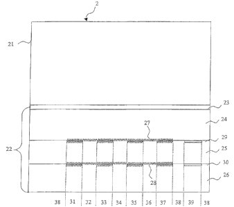
Figure 2a shows a security element for RF identification, which is
formed by a film element 2. The film element 2 is a stamping film. It is
however also possible that the film element 2 is a transfer, sticker or
laminating film or that a security element according to the invention is
formed by the transfer layer portion of a stamping, transfer or laminating
film. The film element 2 has a carrier film 21 and a transfer layer portion
22. The transfer layer portion 22 has a release and/or protective lacquer
layer 23, two replication layers 24 and 25, two electrically conducting
layers 29 and 30 and an adhesive layer 26. The carrier layer 21 comprises
for example a polyester film of a thickness of 12 m to 50 m. The release
and/or protective lacquer layer 23 is applied in a layer thickness of 0.3 to
CA 02531993 2006-01-09
11
1.2 m to the carrier film. The replication layers 24 and 25 are of a layer
thickness of 20 m or less.
The replication layer 24 preferably involves a transparent
thermoplastic material which is applied for example by means of a printing
process to the film body formed by the carrier film 21 and the protective
lacquer and/or release layer 24. After drying, a relief structure 27 is
replicated into the replication layer 24 by means of a stamping tool, in the
regions 31 to 37. It is however also possible here for the replication
operation to be carried out by means of a UV replication process in which a
UV replication lacquer is applied to the film body formed by the carrier film
21 and the release and/or protective lacquer layer 23 and then partially
irradiated with UV light for replication of the relief structure 27. After
replication of the relief structure 27 the replication lacquer hardens by
cross-linking or in some other fashion. The thin, electrically conducting
layer 29 is now applied to the replication layer 24 over the full surface area
involved, in a layer thickness of 50 nm to 50 m, preferably 1 m to 10 m,
for example by vapour deposition or by sputtering or printing. In that case
the electrically conductive layer preferably comprises a metal layer, for
example of copper, aluminium, gold, silver or brass. The conductive layer
can also comprise an alloy of the above-mentioned materials or another
conductive material, for example a conductive polymer.
The electrically conductive layer is then partially demetallised in the
regions 38, 32, 34 and 36 so that for example the conductor track
configuration shown in Figure 2b is afforded in the regions 31 to 37. In that
case demetallisation can be effected by printing on an etching resist and
then etching, by printing on an etching agent or by printing on a washing
mask prior to coating and a washing operation after coating. It will be
appreciated that it is also possible for the vapour deposition operation to be
already effected partially and in pattern form in the configuration shown in
Figures 2a and 2b, by suitably shaped vapour deposition masks. Further
processes are the exposure of photoresist with following etching or laser
ablation.
CA 02531993 2007-12-19
12
The replication layer 25 is then applied, in which a relief structure 28
is then replicated, as already described hereinbefore in relation to the
layers 24 and 29, and then the electrically conductive layer is applied in
partial and pattern-shaped form, as shown in Figure 2a. The adhesive layer
26 is then applied. The adhesive layer 26 is for example a thermally
activatable adhesive.
It would also be possible here to dispense with the replication layer
25 and the electrically conductive layer 30. It will be appreciated that it is
also possible for the film body 2 to have still further layers which for
example afford optically perceptible security features. Thus the film body
can also have for example a thin film layer system for producing viewing
angle-dependent colour shifts, by means of interference.
Figure 2b now shows a portion of the film element 2 with a surface
region 4. The electrically conductive layer 29 is shaped out in the surface
region 4, in the form of a planar coil with two turns, as shown in Figure 2b.
The coil is here for example of the following dimensions: the length
of the coil is 8 cm, the width of the coil is 5 cm, the width of the turns is
2
mm, the spacing between the turns is 2 mm and the thickness of the
electrically conductive layer, depending on the respective choice of the
relief structure 27, is between 50 nm and 10 gm.
In order now to achieve a quality factor Q of 50, a coil resistance R is
to be selected, for which the following applies:
R=50.
C
Accordingly a thickness to of the electrically conductive layer 29 is to
be selected, in respect of which the following condition applies:
p=l C
to = -
w=F=50 L
wherein p is the specific resistance, I is the total length of the conductor
track of the coil, and F is the fractal factor. The fractal factor F is the
ratio
of the effective width to the projected width of the conductor tracks of the
coil.
CA 02531993 2007-12-19
13
The skin effect which changes the resistance at high frequencies is
also to be considered here. In this respect the skin depth Ds is determined
by the following formula:
Ds = 1
n- 71U
wherein la is the permeability of the material and a is electrical
conductivity.
At carrier frequencies in the region of 13.56 MHz and with a
thickness for the electrically conductive layer which is markedly less than
20 lam, the skin effect is negligible. At higher frequencies, for example in
the 895 MHz or 2.45 GHz band in contrast the skin effect also has an action
even with layer thicknesses in respect of the electrically conductive layer in
the range of 1 gm to 50 nm. The resistance of the coil is reduced by virtue
of the skin effect with the increase in surface area which is achieved by the
relief structure 27.
The surface region 4 has four partial regions 41 to 44 in each of
which the orientation of the relief structure 27 is respectively different.
Thus the grooves of the relief structure 27 are oriented horizontally in the
partial regions 41 and 43 and perpendicularly in the partial regions 44 and
42. That provides that the grooves of the relief structure 27 are oriented
very substantially lengthwise of the direction of flow of the electric
current.
The relief structure shown in Figure 2c is used as the profile shape
for the relief structure 27.
Figure 2c shows a portion of a conductor track of the coil, which is of
a width 45 and in which the relief structure 27 is shaped. In this case the
relief structure 27 has a grating period 47 and a profile depth 46. The
fractal factor F now results from the ratio of the effective width which is
determined by the grating period 47 and the relief depth 46 and the
projected width, that is to say the width 45. For a sawtooth profile the
fractal factor is calculated as follows:
F=h/d+ h2+d2
d
wherein h = the height and d = the period.
CA 02531993 2006-01-09
14
Therefore, for the sawtooth-shaped relief structure shown in Figure
2c, with a profile depth of 1 m there is a fractal factor of 1.62 with a
grating period of 2 m, a fractal factor of 2.41 with a grating period of 1 m
and a fractal factor of 4.24 with a grating period of 0.5 m.
In order now to achieve a quality factor of 100 in the above-
described coil, the layer thickness of the electrically conductive layer
without relief structure is to be selected at a value of 1.43 m, when using
a relief structure with a fractal factor of 1.62 it is to be selected at a
thickness of 0.88 m, with a fractal factor of 2.41 it is to be selected at a
thickness of 0.59 m and with a fractal factor of 4.24 it is to be selected at
a value of 0.32 m. As can be seen therefrom therefore the quality factor
and the layer thickness to be selected for the electrically conductive layer
27 are quite substantially influenced by the relief structure 27.
Figures 3 and 4 now show further possible ways of positioning and
shaping out a relief structure 27 in the surface region 4.
Figure 3 shows a surface region 51 and a relief structure 52. As
indicated in Figure 3 the grooves of the relief structure 52 are arranged in
the form of concentric rectangles. Now, the conductor tracks of the coil are
provided in the region in which the relief structure 52 is shaped so that the
relief structure 52 is provided not only in the region of the conductor tracks
but also in the intermediate spaces therebetween. That has the advantage
that the relief structure 52 can be used for different RF components, for
example for coils with a different number of turns.
Figure 4 now shows a surface region 53 having a partial region 54 in
which a relief structure is shaped. In this case the electrically conductive
layer is also provided only in the partial regions 54 so that the relief
structure 'goes over' the regions in which the electrically conductive layer
is
present. In this case, the grooves of the relief structure in the partial
region
54 are respectively oriented in the direction of flow of the electric current
and thus are always oriented in the longitudinal direction of the conductor
tracks forming the coil.
It will be appreciated that any other relief structures can be used as
the relief structure, besides that shown in Figure 2c. Thus for example it is
CA 02531993 2006-01-09
= 15
possible to use relief structures with sinusoidal, rectangular or triangular
profile shapes. The spatial frequency and the profile depth can also be
varied. As already indicated above in that respect in particular spatial
frequencies of between 100 and 2000 lines per mm are particularly well
suitable as that provides for a strong influence in respect of the fractal
factor. In that case the profile depth is preferably selected from the range
of 50nmto10.tm.
In addition it is also possible that, besides the above-indicated
electrical action, the relief structure 27 also produces an optical effect
which can be used for example as an additional security feature of the
security element 2. Thus it is for example possible to deliberately design
structures which have an optical-diffraction effect such as for example
holograms, diffraction gratings, kineforms and the like, which on the one
hand exhibit the above-described electrical effect and also exhibit an optical
action as an additional optical security feature.
Thus for example Figure 5 shows a relief shape 60 which is provided
by a superimposition of a coarse structure with a period 62 and a fine
structure with a period 61. The fine structure can be used here for example
primarily to produce the above-described electrical effects whereas the
coarse structure serves primarily for producing a given optical security
feature. By virtue of such a combination of coarse structure and fine
structure it is then possible for the optimum surface configuration to be
selected for the production of the electrical effect, to be decoupled from the
optical surface configuration necessary for achieving the optical security
feature.
There is also the reverse possibility, that is to say the coarse
structure serves primarily for producing the optical effect and the fine
structure serves primarily for producing the electrical effect.
Figures 6a to 6c show surface regions 63, 64 and 65 in which an
electrically conductive layer is respectively shaped to form an RF antenna.
The surface region 63 has partial surfaces 631 to 634, in each of
which an electrically conductive layer is applied on a relief structure. That
relief structure is oriented in the perpendicular direction in the partial
CA 02531993 2007-12-19
16
regions 631 and 632 and in the horizontal direction in the partial regions
633 and 634.
The surface region 64 has partial surfaces 641 to 647, in each of
which an electrically conductive layer is applied on a relief structure. In
this
case the relief structure is oriented perpendicularly in the partial regions
642, 644 and 647 and horizontally in the partial regions 641, 643, 645 and
646.
The surface region 65 has an electrically conductive layer applied on
a relief structure, in partial regions 651 to 660. The relief structure is
oriented perpendicularly in the partial regions 652, 654, 655, 657 and 659
and horizontally in the partial regions 651, 653, 656, 658 and 660.
In regard to the other shaping of the relief structures attention is
directed to Figure 2c, Figure 3 and Figure 4.
Figure 7a shows a security element 7 having a substrate layer 71, an
RF antenna coil 72 and a capacitive element 70.
The RF antenna coil 72 is of a configuration like the RF antenna coil
12 shown in Figure la or the coil in the surface region 4 shown in Figure 2b
and 2c. The precise structure of the capacitive element 70 is shown in
Figure 7b.
Figure 7b shows a section through the capacitive element 70 and
shows two electrically conductive layers 73 and 76, two replication layers
74 and 75 and a carrier layer 80. The electrically conductive layers 73 and
76 as well as the replication layers 74 and 75 are of a configuration like the
electrically conductive layers 29 and 30 and the replication layers 24 and
25 of Figure 2a. The carrier layer 80 is for example a polyester film or a
bonding layer. It would however also be possible to dispense with the layer
80. The capacitance 70 is further connected to the RF antenna coil 72 by
way of connecting elements 77. As shown in Figure 7b a relief structure 78
and 79 respectively is shaped in the electrically conductive layers 73 and
76.
The capacitance C of the capacitive element 70 is determined as
C_ KEOA
d5
CA 02531993 2006-01-09
17
wherein K is the dielectric constant, o is the permeability constant, A is
the
surface area of the capacitor plates and d5 is the distance between the
capacitor plates. In this embodiment K is 2.1 to 2.3, so is approximately 8.9
= 1012 coul2/N-m2 and d5 is approximately 20 um.
In this case also the relief structures 78 and 79 afford the affect of
increasing the effective surface area, as discussed with reference to Figure
2c, so that in this case also, in the foregoing formula, the surface area A is
to be multiplied by the fractal factor. If, as shown in Figure 7, a relief
structure is shaped in the electrically conductive layer on both sides, then
i0 the surface area A is to be multiplied by the fractal factors of both
relief
structures. If the relief structures 78 and 79 have for example a relief
depth of 1 um and a grating period of 1 um, then the surface area is to be
multiplied by the fractal factor 2.41 x 2.41 = 5.81.
In that way it is possible for the surface area requirement of the
capacitive element to be considerably reduced by means of the relief
structures 78 and 79, or it is possible for the capacitance of the capacitive
element to be adjusted for tuning of the resonance frequency by means of
a specific configuration of the relief structures 78 and 79, with a
predetermined surface area:
(fo = 1
2n LC)
In this case also, as already described above, there is the possibility
that the relief structures 78 and 79 not only serve to influence the
electrical
properties of the capacitive element 70 but also produce optical effects
which are used as an optical security element.
Figure 8a now shows a further embodiment of the invention in which
the processes illustrated with reference to Figures la and 7a are combined
with a configuration of the capacitive element, in which the capacitive
element is formed from a plurality of capacitive partial elements connected
by way of connecting tracks. Thus Figure 8a shows a security element 8
having an RF antenna coil 81, a plurality of capacitors C1 to C7 and a
plurality of connecting tracks which connect the RF antenna coil 81 to the
capacitors C1 to C6. By targetedly severing the connecting tracks it is later
CA 02531993 2006-01-09
= 18
possible to alter the capacitance of the capacitive element afterwards and
thus alter the resonance frequency of the RF resonator circuit.
Thus it is for example possible, as shown in Figure 8b, for the
capacitors C1 to C3 to be connected in a series circuit with the inductance L
formed by the RF antenna coil 81 by targetedly severing connecting tracks,
thereby producing a resonator circuit 82. In addition it is possible, as shown
in Figure 8c, to connect the capacitors C1 to C3 in a parallel circuit by
targetedly severing the connecting tracks. That affords a resonance circuit
83 in which the sum of the partial capacitors C1 to C3 is disposed in
opposite relationship to the inductance L of the RF antenna coil 81.
As can be seen therefrom a plurality of different capacitance values
can be achieved afterwards by targetedly severing the connecting tracks so
that a personalised, unique frequency can be afterwards encoded in the
security element 8. The operation of severing the connecting paths is
effected here for example by means of a laser.
Reference will now be made to Figures 9a to 9b to discuss further
possible options in regard to the configuration of a security element for RF
identification according to the invention.
Figure 9a shows a security element 91. That security element has an
inductance and a capacitance which are connected to form a resonance
circuit. A microchip is not provided here. Such a security element serves for
example as an anti-theft means and reacts to a quite specific carrier
frequency.
Figure 9b shows a security element 92 which has an inductance and
a capacitance. The capacitance can be individualised by means of the
process described with reference to Figure 8a so that this security element
responds to a given, personalised frequency. Such a security element can
be used for example for identification and authentication.
Figure 9c shows a security element 92 in which a coil is connected to
various capacitances in such a way that various resonance circuits are
afforded and the circuitry accordingly has two or more resonance
frequencies. Subsequent removal of individual connecting tracks makes it
possible to encode items of information by determining the resonance
CA 02531993 2006-01-09
19
frequencies which that circuit has. Thus for example when using eight
different resonance frequencies 28 - 1 encoding options are possible. Such a
security element can be used for identification and authentication purposes.
Figure 9d shows a security element 93 having an antenna and a
microchip 94. The communication between the transponder and the reading
device can lie in the communication of a simple ID identification or a
process in which data stored in the transponder are identified and stored
afresh. Such an element can read and write data and communicate with a
reading device so that it is possible here to implement complex functions,
in particular complex identification, authentication, e-commerce and e-
government functions.