Note: Descriptions are shown in the official language in which they were submitted.
CA 02532298 2006-01-11
WO 2005/011058 PCT/US2004/022808
METHOD AND APPARATUS FOR FORMING MILLIMETER WAVE PHASED
ARRAY ANTENNA
FIELD OF THE INVENTION
[0001) The present invention relates to antennas, and more
particularly to an electronically scanned, dual beam phased array antenna
capable of operating at millimeter wavelengths and incorporating a corporate
stripline waveguide structure.
BACKGROUND OF THE INVENTION
[0002] A phased array antenna is composed of multiple radiating
antenna elements, individual element control circuits, a signal distribution
network, signal control circuitry, a power supply, and a mechanical support
structure. The total gain, effective isotropic radiated power and scanning and
side lobe requirements of the antenna are directly related to the number of
elements in the antenna aperture, the element spacing, and the performance
of the elements and element electronics. In many applications, thousands of
independent element/control circuits are required to achieve a desired
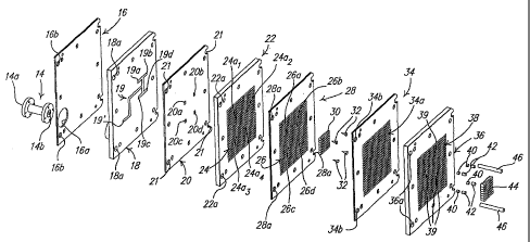
antenna performance. A typical phased array antenna includes independent
electronic packages for the radiating elements and control circuits that are
interconnected through an external distribution network. Figure 1 shows a
schematic of a typical transmit phased array antenna which includes an input,
distribution network, element electronics and radiators.
[0003] As the antenna operating frequency increases, the required
spacing between radiating elements decreases and it becomes difficult to
physically configure the control electronics and interconnects within the
increasingly tight element spacing. Relaxing the tight element spacing will
degrade the beam scanning performance, but adequately providing multiple
interconnects requires stringent manufacturing and assembly tolerances
which increase system complexity and cost. Consequently, the performance
and cost of the phased array antenna depends primarily on module packaging
and distribution network interconnects. Multiple beam applications further
1
CA 02532298 2006-01-11
WO 2005/011058 PCT/US2004/022808
complicate this problem by requiring more electronic components and
interconnects within the same antenna volume.
[0004] Phased array packaging architectures can be divided into tile
(i.e., coplanar) and brick (i.e., in-line) styles. Figure 2 shows a typical
tile-type
architecture which exhibits components that are co-planar with the antenna
aperture and which are assembled together as tiles. Figure 3 shows a typical
brick-type architecture which uses in-line components that are perpendicular
to the antenna aperture and are assembled together similar to bricks.
[0005] The assignee of the present application, The Boeing
Company, has been a leading innovator in phased array module/element
packaging technology. The Boeing Company has designed, developed and
delivered many phased arrays which use tile, brick and hybrid techniques to
fabricate radiator modules and/or distribution networks. The RF distribution
network which provides electromagnetic wave EM energy to each of the
phased array modules can be delivered in what is called "series" or
"parallel".
Series distribution networks are often limited in instantaneous bandwidth
because of the various delays which the EM wave signal experiences during
the distribution. Parallel networks, however, provide "equal delay" to each of
the modules, which allows wide instantaneous bandwidth. However, parallel
distribution increases in difficulty with a large number of radiator modules.
The most common method to deliver equal delay to a group of phased array
modules is a "corporate" distribution network. The corporate distribution
network uses binary signal splitters to deliver equally delayed signals to 2"
modules. This type of distribution lends itself well to the tile array
architecture
that has been used extensively throughout industry.
[0006] The use of a corporate network in a tile architecture is limited
by the module spacing. It becomes increasingly more difficult to distribute EM
wave energy, DC power signals, and logic signals with tightly-packed modules
of wide-angle beam scanning arrays at higher operating frequencies.
Because the cost of RF power also increases with operating frequency,
designers try to limit distribution losses by using low-loss transmission
media.
The lowest loss medium used is an air filled rectangular waveguide.
2
CA 02532298 2006-01-11
WO 2005/011058 PCT/US2004/022808
However, such a waveguide requires a large volume and is not easily routed
to individual sites (i.e., antenna modules). Stripline conductors, depending
on
material parameters and dimensions, can exhibit as much as 5-10 times the
amount of loss per unit length of waveguide as an air filled rectangular
waveguide. However, a stripline waveguide is very compact and readily able
to distribute RF energy to tightly-packed modules (i.e., radiating elements)
that are separated by only a very small amount of spacing.
[0007] Air filled waveguides can be used exclusively in a series
network to feed tightly packed antenna modules. Each air filled length of
waveguide uses a series of slots in what is referred to as a "rail". The
electrical length between the slots in a rail changes with the operating
frequency. If the rail is used to form an antenna beam, the change in
electrical length between slots causes the beam to shift or "squint" away from
the intended angle as the operating frequency changes. As the number of
slots in the rail is increased, the beam squint becomes more pronounced, thus
reducing the instantaneous bandwidth even further. The slots in a rail also
tend to interact with each other and make rail designs more difficult and
complex. If the slots were isolated from each other, then the length of each
slot needed for the desired coupling levels could be more easily determined.
A rail also achieves its desired phase and amplitude distribution at a single
center frequency and quickly degrades as the operating frequency deviates
away from the center frequency.
[0008] For a phased array antenna, the phase errors introduced by
series distribution networks can be adjusted for in the antenna module using
phase shifters. To accomplish the adjustment or calibration, a priori
knowledge of the instantaneous operating frequency is required. A look-up
table is used to correct for the beam squint at various frequency points along
the operating bandwidth of the array. The length of the rail determines the
number of steps or increments required to adequately adjust the phase
shifters. Longer rails cause more beam squint and narrower instantaneous
bandwidth, which means that more frequency increments are required to
calibrate the numerous antenna modules of the antenna.
3
CA 02532298 2009-11-30
[0009] A particularly challenging problem that The Boeing Company
has been faced with, and which the antenna and method of the present invention
overcomes, is developing a wide-beam scanning, Q-band phased array antenna
capable of operating at 44 GHz for MILSTAR communications. The MILSTAR
communication protocol uses narrowband bursts of information frequency hopping
over the 2 GHz bandwidth of operation. However, the use of a series fed
waveguide and the differing beam squints requires knowledge of the next beam
hopping frequency so that the appropriate delay can be obtained from the look-
up
table and applied to the phase shifters. Without such knowledge of the next
beam
hopping frequency, the series fed beam rail squints cannot be accurately
determined. For security reasons, it is desirable for a phased array antenna
system to not require specific frequency information for operation but instead
to be
able to operate over the entire bandwidth as a passive device. A new form of
corporate feed waveguide network is therefore required which allows very tight
module spacing, but which still does not require individual series fed rail
beams
squints to be calculated to maintain calibration of all of the individual
module
elements of the antenna.
SUMMARY OF THE INVENTION
[0010] An aspect of the present invention is directed to a phased array
antenna system and method which is capable of operating at 44 GHz and in
accordance with the MILSTAR communication protocol without advance
knowledge of the next beam hopping frequency. Systems and methods are
provided to accomplish this by providing a phased array antenna incorporating
the
use of a new waveguide network. A first air filled waveguide structure feeds
electromagnetic wave (EM) input energy into a second, dielectrically-filled
waveguide structure. The second, dielectrically-filled waveguide structure
feeds
EM wave energy into a corporate stripline waveguide network. The corporate
stripline waveguide network distributes the EM wave energy to a plurality of
radiating elements of each of a corresponding plurality of independent antenna
modules making up the phased array antenna.
[0011] In one aspect, the first waveguide structure comprises a
rectangular air waveguide structure. This structure feeds EM wave input energy
4
CA 02532298 2009-11-30
from an input thereof into a plurality of outputs and divides the EM wave
energy
among the plurality of outputs. These outputs feed the second waveguide
structure which, in one apsect, includes a plurality of dielectrically-filled
circular
waveguides. The second waveguide structure channels the EM wave energy to a
corresponding plurality of inputs of the stripline waveguide structure where
this EM
wave energy is further successively divided before being applied to each of
the
radiating elements of the plurality of antenna modules of the antenna system.
The
use of the corporate stripline waveguide structure allows extremely tight
element
spacing to be achieved with only a very small reduction in efficiency of the
system.
The use of the corporate stripline waveguide structure further eliminates the
need
to apply independent beam squint corrections that would necessitate knowing
the
next beam hopping frequency in a MILSTAR application. The use of the corporate
stripline waveguide network, in connection with the use of the first and
second
waveguide structures and suitable phase shifters, effectively provides the
same
delay to each radiating element of the antenna system, which also
significantly
simplifies the complexity of the electronics needed for the antenna system.
[0012] Advantageously, the antenna system in one aspect of the present
invention is calibrated using a single look-up table; therefore, a prior
knowledge of
the next beam hopping frequency is not needed. The antenna system provides
excellent beam side lobe levels at both boresight and at a 60 degree scan
angle.
The beam patterns produced by the antenna system also exhibit excellent cross-
polarization levels.
[0012a] In accordance with one aspect of the invention there is
provided a phased array antenna. The phased array antenna includes a first
dielectric filled waveguide structure for dividing an input of electromagnetic
(EM)
wave energy into a first plurality of EM wave signals, and a second dielectric
filled
waveguide structure disposed adjacent the first dielectric filled waveguide
structure
having a plurality of generally circular dielectric filled waveguides for
receiving
each of the first plurality of EM wave signals and channeling the first
plurality of EM
wave signals toward an output end of each one of the plurality of dielectric
filled
waveguides. The phased array antenna also includes a stripline waveguide
circuit
board positioned adjacent the second dielectric filled waveguide structure and
having circuit traces forming a plurality of inputs overlaying the output ends
of the
5
CA 02532298 2009-11-30
[0012b] dielectric filled waveguides, the stripline waveguide circuit
board distributing the EM wave signals via the circuit traces to a plurality
of closely
spaced EM wave radiating elements.
[0012c] The first dielectric waveguide structure may form a 1X4
dielectric filled waveguide structure.
[0012d] The stripline waveguide circuit board may include a plurality of
binary signal splitters for equally distributing EM wave energy from the EM
wave
signals to each of the EM wave radiating elements.
[001 2e] The phased array antenna may include a third waveguide
structure having a plurality of dielectric filled waveguides disposed to
receive
radiation from each of the plurality of closely spaced EM wave radiating
elements.
[00121] A portion of EM wave energy radiated by each of the EM wave
radiating elements may be radiated back toward the second dielectric filled
waveguide structure and the phased array antenna may further include a
plurality
of reflectors each being associated with one of the EM wave radiating elements
and disposed to reflect the portion of the EM wave energy back toward the
plurality
of dielectric filled waveguides of the third waveguide structure.
[0012g] The phased array antenna may include a reflector disposed
adjacent to each of the plurality of inputs of the stripline waveguide circuit
board,
the reflector being operably configured to reflect EM wave energy that passes
the
input of the stripline waveguide circuit board back toward the input.
[0012h] In accordance with another aspect of the invention there is
provided a phased array antenna. The phased array antenna includes a first
dielectric filled waveguide structure for dividing an input of electromagnetic
(EM)
wave energy into a first plurality of EM wave signals, and a second dielectric
filled
waveguide structure having a plurality of dielectric filled, generally
circular
waveguides for receiving each of the first plurality of EM wave signals at
inputs
ends thereof and channeling the first plurality of EM wave signals toward
output
ends of the plurality of dielectric filled waveguides. The phased array
antenna also
includes a stripline waveguide distribution circuit disposed generally
parallel to and
adjacent the second dielectric filled waveguide structure for receiving the EM
wave
signals and further dividing and further distributing EM wave energy therefrom
to a
plurality of EM wave radiating elements.
5a
CA 02532298 2009-11-30
[0012i] The stripline waveguide distribution circuit may include a
plurality of signal traces forming signal paths, with a plurality of input
traces of the
signal traces communicating with the generally circular waveguides to receive
and
channel the EM wave signals into the stripline waveguide distribution circuit.
[0012j] The first dielectric filled waveguide structure may form a 1X4
corporate waveguide structure.
[0012k] The stripline waveguide distribution circuit may include a
plurality of binary signal splitters for dividing the EM wave signals as the
EM wave
signals are routed through the stripline waveguide distribution circuit.
[00121] The first dielectric filled waveguide structure may include an
air filled rectangular waveguide.
[0012m] The phased array antenna may include a third waveguide
structure disposed adjacent to the stripline waveguide circuit board and
having a
plurality of dielectric filled waveguides for receiving radiation from each of
the
plurality of closely spaced EM wave radiating elements.
[0012n] A portion of EM wave energy radiated by each of the EM wave
radiating elements may be radiated back toward the second dielectric filled
waveguide structure and the phased array antenna may further include a
plurality
of reflectors each being associated with one of the EM wave radiating elements
and disposed to reflect the portion of the EM wave energy back toward the
plurality
of dielectric filled waveguides of the third waveguide structure.
[00120] The phased array antenna may include a reflector disposed
adjacent to each of the plurality of inputs of the stripline waveguide circuit
board,
the reflector being operably configured to reflect EM wave energy that passes
the
input of the stripline waveguide circuit board back toward the input.
[0012p] In accordance with another aspect of the invention there is
provided a millimeter wave phased array antenna. The phased array antenna
includes a corporate waveguide feed for evenly dividing an input
electromagnetic
(EM) wave signal to a sub-plurality of EM wave signals, and a dielectric
filled
waveguide structure forming a plurality of generally circular, dielectric
filled
waveguides for receiving the sub-plurality of EM wave signals and channeling
the
sub-plurality of EM wave signals to output ends of the dielectric filled
waveguides.
The phased array antenna also includes a stripline waveguide structure
overlaying
5b
CA 02532298 2009-11-30
the dielectric filled waveguide structure for further dividing and
distributing EM
wave energy from the EM wave signals to a plurality of radiating elements.
[0012q] The corporate waveguide structure may include a 1X4, air
filled corporate waveguide feed.
[0012r] The stripline waveguide structure may include a plurality of
input traces each electrically coupled with an associated one of the generally
circular dielectric filled waveguides.
[0012s] The stripline waveguide structure may include a plurality of
binary signal splitters for dividing the EM wave signals prior to applying the
EM
wave signals to the radiating elements.
[0012t] The phased array antenna may include a third waveguide
structure having a plurality of dielectric filled waveguides disposed to
receive
radiation from each of the plurality of closely spaced EM wave radiating
elements.
[0012u] A portion of EM wave energy radiated by each of the EM wave
radiating elements may be radiated back toward the dielectric filled waveguide
structure and the phased array antenna may further include a plurality of
reflectors
each being associated with one of the EM wave radiating elements and disposed
to reflect the portion of the EM wave energy back toward the plurality of
dielectric
filled waveguides of the third waveguide structure.
[0012v] The phased array antenna may include a reflector disposed
adjacent to each of the plurality of inputs of the stripline waveguide circuit
board,
the reflector being operably configured to reflect EM wave energy that passes
the
input of the stripline waveguide circuit board back toward the input.
[0012w] In accordance with another aspect of the invention there is
provided a method for forming a phased array antenna. The method involves
using a corporate waveguide feed for evenly dividing an input electromagnetic
(EM) wave signal into a plurality of EM wave signals, channeling the plurality
of EM
wave signals through a plurality of generally circular dielectric filled
waveguides,
and using a stripline waveguide in communication with the dielectric filled
waveguides for further dividing and distributing the EM wave signals to a
plurality
of radiating elements.
5c
CA 02532298 2009-11-30
[0012x] Using a corporate waveguide may involve using a 1X4
corporate waveguide for evenly dividing the EM wave signal into a plurality of
four
EM wave signals.
[0012y] Using a stripline waveguide may involve using a plurality of
binary signal splitters to further evenly divide the plurality of EM wave
signals to a
plurality of antenna radiating elements.
[0012z] The method may involve receiving radiation from each of the
EM wave radiating elements at respective dielectric filled waveguides disposed
adjacent to the stripline waveguide.
[0012aa] A portion of EM wave energy radiated by each of the EM wave
radiating elements may be radiated back toward the plurality of generally
circular
dielectric filled waveguides and the method may further involve reflecting the
portion of the EM wave energy back toward the respective dielectric filled
waveguides disposed adjacent to the stripline waveguide.
[0012bb] The method may involve reflecting EM wave energy that
passes an input of the stripline waveguide back toward the input.
[0012cc] In accordance with another aspect of the invention there is
provided a method of using a phased array antenna. The method involves
generating an electromagnetic (EM) wave input signal, and directing the EM
wave
input signal into an input of a corporate waveguide the EM wave input signal
is
divided into a first sub-plurality of EM wave signals. The method also
involves
channeling the first sub-plurality of EM wave signals into a dielectric filled
waveguide structure having a corresponding plurality of generally circular
dielectric
filled waveguides, and coupling the first sub-plurality of EM wave signals
into a
stripline waveguide structure. The EM wave energy of the first sub-plurality
of EM
wave signals is further successively divided into a second sub-plurality of EM
wave
signals. The method also involves applying the second sub-plurality of EM wave
signals to a corresponding plurality of antenna elements.
[001 2dd] Coupling the first sub-plurality of EM wave signals into a
dielectric filled waveguide structure may further involve using a plurality of
binary
signal splitters to successively divide the first sub-plurality of EM wave
signals.
[0012ee] Using the corporate waveguide may involve using a 1X4
corporate waveguide.
5d
CA 02532298 2009-11-30
[0012ff] The method may involve receiving radiation from each of the
plurality of antenna elements at respective dielectric filled waveguides
disposed
adjacent to the stripline waveguide structure.
[001 2gg] A portion of EM wave energy radiated by each of the plurality
of antenna elements may be radiated back toward the dielectric filled
waveguide
structure and the method may further involve reflecting the portion of the EM
wave
energy back toward the plurality of dielectric filled waveguides disposed
adjacent
to the stripline waveguide structure.
[001 2hh] The method may involve reflecting EM wave energy that may
be not coupled into the stripline waveguide back toward the stripline
waveguide.
[0013] Further areas of applicability aspects of the present invention
will become apparent from the detailed description provided hereinafter. It
should
be understood that the detailed description and specific examples are
5e
CA 02532298 2006-01-11
WO 2005/011058 PCT/US2004/022808
intended for purposes of illustration only and are not intended to limit the
scope of the invention.
BRIEF DESCRIPTION OF THE DRAWINGS
[0014] The present invention will become more fully understood
from the detailed description and the accompanying drawings, wherein:
[0015] Figure 1 is a simplified block diagram of a typical transmit
phased array antenna system;
[0016] Figure 2 is a simplified perspective view of certain of the
components of a tile-type phased array antenna system;
[0017] Figure 3 is a simplified perspective view of certain
components of a brick-type phased array antenna system;
[0018] Figure 4 is a simplified perspective view of a phased array
antenna in accordance with a preferred embodiment of the present invention;
[0019] Figure 5 is an exploded perspective view of the antenna
system feed network of Figure 4;
[0020] Figure 5A is a partial cross-sectional view of a tapered
transition dielectric plug inserted within the tapered transmission plate and
the
WDN feed plate;
[0021] Figure 6 is a plan view of the waveguide distribution network
input plate which forms a 1 X4 air filled rectangular waveguide feed
structure;
[0022] Figure 7 is an enlarged plan view of the stripline waveguide
printed circuit board;
[0023] Figure 8 is a highly enlarged portion of the circuit board of
Figure 7;
[0024] Figure 9 is a graph of the far-field amplitude of the antenna
of the present invention at a zero degree scan angle (i.e., along the
boresight); and
[0025] Figure 10 is a graph of the far-field amplitude of the antenna
system of the present invention at a 60 degree scan angle.
6
CA 02532298 2006-01-11
WO 2005/011058 PCT/US2004/022808
DETAILED DESCRIPTION OF THE PREFERRED EMBODIMENTS
[0026] The following description of the preferred embodiment(s) is
merely exemplary in nature and is in no way intended to limit the invention,
its
application, or uses.
[0027] Referring to Figure 4, an antenna system 10 in accordance
with a preferred embodiment and method of the present invention is shown.
The antenna system 10 forms an antenna able to operate at millimeter
wavelengths, and more particularly at 44 GHz (Q-band) and in accordance
with the MILSTAR protocol without requiring advance knowledge of the next
beam hopping frequency being employed in a MILSTAR application. The
antenna system 10 forms a dual beam system having a plurality of 524
independent antenna modules very closely spaced relative to one another to
enable operation at millimeter wave frequencies, and more preferably at about
44 GHz, without suffering significant beam degradation and performance at
scan angles up to (or exceeding) 60 degrees. The antenna system generally
includes a chassis 11 within which is supported a feed network 12 and
associated electronics (not shown).
[0028] Referring to Figure 5, an exploded perspective view of the
major components of the feed network 12 of the antenna system 10 is
illustrated. The EM wave input signal is generated by a microwave generator
(not shown) to an input end 14a of a waveguide input transition member 14.
The EM wave signal travels through a rectangular bore to a rectangular output
14b. The waveguide input transition member 14 is inserted through an
aperture 16a in a rear, mechanical, co-thermal spacer plate 16 and the output
14b is connected to a waveguide distribution network (WDN) input plate 18.
The WDN input plate 18 has a waveguide 19 having an input 19' and outputs
19a-19d. The WDN input plate 18 is coupled to a bottom rectangular feed
plate 20 having a plurality of four rectangular waveguide slots 20a-20d that
align with outputs 19a-19d. The EM wave input signals are channeled from
the WDN input plate 18 through waveguide 19, through slots 20a-20d and into
a WDN tapered transmission plate 22. Transmission plate 22 has a plurality
of 524 generally circular recesses 24 that do not extend completely through
7
CA 02532298 2006-01-11
WO 2005/011058 PCT/US2004/022808
the thickness of plate 22. Plate 22 also includes four apertures 24a1 - 24a4
that extend completely through the plate 22. The four apertures 24a1 - 24a4
are aligned with the four waveguide slots 20a-20d. Each one of the 524
recesses 24 and four apertures 24a1 - 24a4 are longitudinally aligned with a
corresponding plurality of apertures 26 in a WDN feedplate 28. A plurality of
524 1/4 wave, circular backshort dielectric plugs 30 (shown merely as a
representative plurality in Figure 5) fill 524 of the apertures 26 and also
fill 524
of the apertures 24 of transmission plate 22. A plurality of four tapered
transition dielectric plugs 32 extend through four of the apertures 26a-26d.
The apertures 26 filled by tapered transition dielectric plugs 32 are those
apertures that are longitudinally aligned with apertures 24a1 - 24a4 of
tapered
transmission plate 22 and rectangular slots 20a-20d of rectangular feed plate
20. Dielectric plugs 32 also extend partially into apertures 24a1-24a4 when
the feed network 12 is fully assembled. This is illustrated in Figure 5a where
plug 32 can be seen to have a circular head portion 32a and a conical body
portion 32b. The circular head portion 32a fills an associated aperture (i.e.,
one of apertures 26a-26d) in the WDN feedplate 28 and the conical body
portion 32b rests within an associated one of the apertures 24a1-24a4 in the
WDN tapered transmission plate 22.
[0029] The apertures 24a1-24a4 in the WDN tapered transmission
plate 22 begin as rectangular in cross section on the back side of
transmission plate 22 (i.e., the side not visible in Figure 5), and transition
into
a circular cross sectional shape on the side visible in Figure 5. This,
together
with the conical portions of plugs 32, serves to provide a rectangular-to-
circular waveguide transition area for the EM wave energy traveling through
the plate 22. In one preferred form plugs 32 have a dielectric constant of
preferably about 2.5. Accordingly, WDN transmission plate 22 functions as a
rectangular-to-circular waveguide transitioning component.
[0030] With further reference to Figure 5, a WDN stripline printed
circuit board (PCB) 34 is secured over an output side of WDN feedplate 28
and forms a means for dividing the EM wave energy channeled through each
of the four-apertures 24a to a corresponding input trace of a corporate
8
CA 02532298 2006-01-11
WO 2005/011058 PCT/US2004/022808
stripline distribution network 34a formed on the WDN stripline PCB 34. A
WDN circular waveguide plate 36 is secured over the WDN stripline PCB 34.
WDN circular waveguide plate 36 includes 528 circular apertures, designated
generally by reference numeral 38, with four apertures 39 each filled with one
circular backshort dielectric plug 40 and one circular backshort aluminum
(conductive) plug 42. The filled apertures 39 are those that are
longitudinally
aligned with slots 20a-20d of rectangular feed plate 20 and apertures 24a1-
24a4 of tapered transmission plate 22. The remaining 524 apertures denoted
by reference numeral 38 are filled with circular waveguide dielectric plugs 44
(shown merely as a representative plurality in Figure 5). Plugs 44 preferably
are comprised of Rexolite plastic. A pair of module alignment pins 46
extend through apertures 36a in waveguide plate 36, apertures 34b in WDN
stripline circuit board 34, apertures 28a in feed plate 28, apertures 22a in
tapered transition plate 22, apertures 21 in rectangular feed plate 20,
apertures 18a in WDN input plate 18 and apertures 16b in spacer plate 16 to
maintain alignment of the large plurality of apertures of the components 22,
28, 34 and 36 illustrated in Figure 5.
[0031] With brief reference to Figure 6, the WDN input plate 18 can
be seen in greater detail. WDN input plate 18 includes the rectangular, air-
filled waveguide 19 having input 19' that receives EM wave energy from the
output end 14b of waveguide input transition 14 of Figure 5. The rectangular,
air-filled waveguide 19 takes this EM wave input energy and divides it
between the four rectangular output slots 19a, 19b, 19c, and 19d. The EM
wave energy exiting through rectangular slots 19a-19d is channeled through
rectangular slots 20a-20d of WDN bottom rectangular feed plate 20 shown in
Figure 5. WDN input plate 18 is preferably formed from a single sheet of
metal, and more preferably from aluminum, although it will be appreciated that
other suitable metallic materials such as gold could be employed. Spacer
plate 16 is also preferably formed from metal, and more preferably aluminum,
as are plates 22, 28 and 38.
[0032] Figure 7 is a plan view of the stripline printed circuit board
34. Input traces 34a1, 34a2, 34a3 and 34a4 are aligned with apertures 24a1-
9
CA 02532298 2006-01-11
WO 2005/011058 PCT/US2004/022808
24a4 of the waveguide tapered transition plate 22, respectively. More
specifically, the input traces 34a1-34a4 are each disposed to line up parallel
with the electromagnetic field in each of apertures 26a-26d. Inputs 34a1-34a4
each feed a plurality of EM wave radiating elements 56 (i.e., independent
antenna modules) through a plurality of "T-junctions" 35 (denoted in Figure 8)
formed by the conductive portions (i.e., stripline traces) of the circuit
board 34.
More specifically, each of the "T-junctions" 35 of the WDN stripline PCB 34
operate as binary signal splitters to successively (and evenly) divide the EM
wave input energy received at each of inputs 34a1-34a4 into smaller and
smaller subpluralities that are eventually applied to each radiating element
56.
Figure 8 illustrates a representative portion of the corporate EM wave
distribution network formed by the stripline PCB 34. Input 34a2 can be seen
to feed radiating elements 56a-56p. Two representative T-junctions 35 are
shown in Figure 8.
[0033] Input 34a1 feeds 254 of the radiating elements 56, input 34a2
feeds 126 of the radiating elements 56, input 34a3 feeds 96 of the radiating
elements 56 and input 34a4 feeds 48 of the radiating elements 56.
[0034] In operation, EM wave energy is radiated by each of the
radiating elements 56 through the apertures 38 in the WDN circular
waveguide plate 36, and also back towards the WDN feed plate 28. The
plugs 30 have a preferred dielectric constant of about 2.5. Electromagnetic
energy travels through plugs 30 and is reflected at the very bottom wall of
each of the 524 recesses in transmission plate 22 back toward circuit board
34 and continuing on through apertures 38 in WDN circular waveguide plate
36. In one preferred form plugs 30 are made from Rexolite plastic material.
Plugs 40, which are preferably comprised of Rexolite plastic, as well as
plugs 42, which are preferably metal, and more preferably aluminum, fill
apertures 39. The EM wave energy from apertures 26a-26d travels through
plugs 40 and is reflected by plugs 42 back towards input traces 34a1 - 34a4 of
the circuit board 34. Plugs 30, 32, 40 and 44 each have a dielectric constant
of preferably about 2.5 and enable operation of the antenna system 10 at
CA 02532298 2006-01-11
WO 2005/011058 PCT/US2004/022808
millimeter wave frequencies with the very tight element spacing used in the
antenna system.
[0035] With brief reference to Figures 9 and 10, the performance of
the antenna system of the present invention can be seen. Referring
specifically to Figure 9, the far-field performance of the antenna system 10
can be seen with the antenna system operating at 44.5 GHz and at a zero
degree scan angle. Referring to Figure 10, the antenna system 10 is shown
operating at 44.5 GHz but with a 60 degree scan angle. The resulting
sidelobe levels, represented by reference numerals 58, are well within
acceptable limits and the beams shown in Figures 9 and 10 exhibit good
cross-polarization levels. Performance is similar across a design bandwidth
of 43.5 - 45.5 GHz.
[0036] The antenna system 10 of the present invention thus enables
a phased array antenna to be formed with the radiating elements 56 being
very closely spaced to one another to be able to perform at millimeter wave
frequencies, and more particularly at 44 GHz. Importantly, the antenna
system 10 does not require knowledge of the next beam hopping frequency
when used in a MILSTAR communications protocol. The corporate WDN
stripline printed circuit board 34 of the antenna system 10 enables the
extremely close radiating element 56 spacing needed for excellent antenna
performance at millimeter wave frequencies while allowing the amplitude and
phased delays applied to each radiating element 56 to be determined from a
single look-up table.
[0037] It will also be appreciated that while the terms "input" and
"output" have been used to describe portions of the components of the
antenna system 10, that this has been done with the understanding that the
antenna has been described in a transmit mode of operation. As one skilled
in the art will readily understand, these terms would be reversed when the
antenna system 10 is operating in a receive mode.
[0038] While various preferred embodiments have been described,
those skilled in the art will recognize modifications or variations which
might
be made without departing from the inventive concept. The examples
11
CA 02532298 2006-01-11
WO 2005/011058 PCT/US2004/022808
illustrate the invention and are not intended to limit it. Therefore, the
description and claims should be interpreted liberally with only such
limitation
as is necessary in view of the pertinent prior art.
12