Note: Descriptions are shown in the official language in which they were submitted.
CA 02532638 2006-O1-16
WO 2005/010964 PCT/US2004/019946
1
SILICON CRYSTALLIZATION USING SELF-ASSEMBLED MONOLAYERS
RELATED APPLICATIONS
[0001] This application claims the priority of United
States Application No. 10/622,606, filed July 18, 2003.
BACKGROUND
[0002] Often in display devices, it is useful to
incorporate electronic components onto a glass substrate
used in the display device. This is especially the case
in flat panel display (FPD) devices such as liquid crystal
displays (LCD's). In LCD devices, a layer of liquid
crystal material is modulated by voltages, which are
controlled using electronic components including
transistor arrays. Typically, the transistors of the
arrays are thin-film transistors (TFT), and are metal
oxide semiconductor (MOS) devices.
[0003] The LCD displays often comprise a glass
substrate with the transistors disposed over the glass
substrate and beneath a layer of LC material. The
transistors are arranged in a patterned array, and are '
driven by peripheral circuitry to provide desired
switching voltages to orient the molecules of the LC
material in the desired manner. Moreover, the transistors
of the array are often formed directly on or over the
glass substrate from a semiconductor material.
[0004] Because the mobility of carriers of a
semiconductor is generally greater in crystalline and
polycrystalline materials compared to amorphous materials,
it is beneficial to grow crystalline structures on or over
CA 02532638 2006-O1-16
WO 2005/010964 PCT/US2004/019946
2
the glass substrate of the LCD display and fabricating the
transistors therefrom. However, for reasons of uniformity
and smoothness, the semiconductor films are typically
deposited in an amorphous state and then converted to a
polycrystalline structure. Typically, these crystalline
structures are polycrystalline structures.
[0005] I~n.own methods of semiconductor crystalline
growth often require annealing a layer of amorphous
semiconductor materials at relatively high. temperatures or
for long time periods. Because the annealing temperatures
for crystal growth are too great for the substrate over
which the semiconductor crystals are formed, or to speed
manufacturing time, other techniques have been explored to
meet this desired end. These techniques include laser
annealing.
[0006] While various techniques have been attempted to
form polycrystalline silicon on glass substrates, there
are deficiencies in both the resultant material's
characteristics and from the perspective of economic
feasibility. As such, what is needed is a method of
fabricating semiconductor materials over substrates and
the structures formed thereby that overcomes at least the
deficiencies of the known techniques.
SUN~lARY
[0007] In accordance with an exemplary embodiment, a
display device comprises a substrate having a
monocrystalline or polycrystalline material disposed
thereover, wherein the substrate has a strain point that
is lower than a forming temperature of the monocrystalline
or polycrystalline material.
CA 02532638 2006-O1-16
WO 2005/010964 PCT/US2004/019946
3
[0008] In accordance with another exemplary embodiment,
a method of fabricating a monocrystalline or
polycrystalline material over a substrate includes
providing a self-assembled monolayer (SAM) over the
substrate, depositing a layer over the SAM, and
substantially crystallizing the layer.
BRIEF DESCRIPTION OF THE DRAWINGS
[0009] The invention is best understood from the
following detailed description when read with the
accompanying drawing figures. It is emphasized that the
various features are not necessarily drawn to scale. In
fact, the dimensions of the various features may be
arbitrarily increased or decreased for clarity of
discussion.
[00010] Fig. 1 is a cross-sectional view of a LCD
display in accordance with an exemplary embodiment.
[00011] Figs. 2a-2e are cross-sectional views of an
illustrative process of forming crystalline structure on a
glass substrate in accordance with an exemplary
embodiment.
[00012] Fig. 3 is a flowchart of an illustrative process
of forming crystalline structure on a glass substrate in
accordance with an exemplary embodiment.
DETAILED DESCRIPTION
[00013] In the following detailed description, for
purposes of explanation and not limitation, exemplary
embodiments disclosing specific details are set forth in
order to provide a thorough understanding of the exemplary
embodiments. However, it will be apparent to one of
ordinary skill in the art that the present invention may
CA 02532638 2006-O1-16
WO 2005/010964 PCT/US2004/019946
4
be practiced in other embodiments that depart from these
specific details. In other instances, detailed
descriptions of well-known devices and methods are omitted
so as to not obscure the description of the present
invention.
[000147 Fig. 1 shows a cross-sectional view of an LCD
display 100 in accordance with an exemplary embodiment.
The display 100 may be of a flat panel display, a head-up
display or similar device. It is noted the embodiments
described may be implemented in applications other than
those specifically mentioned. To wit, the embodiments
specifically disclosed are intended to be illustrative and
not limiting of the applications of the embodiments.
[00015] The display 100 includes a substrate 101, which
may be a glass material suitable for video display
devices. Exemplary materials include, but are not limited
to, Code 1737 and Eag1e2o0o TM glass by Corning
Incorporated, as well as other borosilicate and
aluminosilicate glasses. A layer 102 of monocrystalline
or polycrystalline (poly) material, is formed over the
substrate 101. In an exemplary embodiment layer 102 is a
monocrystalline or polycrystalline semiconductor such as
silicon. Optional barrier layers (not shown) may be
formed between the substrate 101 and layer 102.
Electronic devices (not shown) are fabricated from this
layer 102. In accordance with exemplary embodiments, the
electronic devices are MOS transistors used to selectively
switch on and off voltage sources.
[000167 The layer 102 is fabricated using a self-
assembled monolayer (SAM) that is chosen to introduce a
seeding effect that lowers the crystallization temperature
and speeds the nucleation of seed crystals. This results
CA 02532638 2006-O1-16
WO 2005/010964 PCT/US2004/019946
in relatively large grain sizes at lower temperatures and
in a shorter time period, and/or with. greater film
uniformity, than by known crystal growth techniques. This
is particularly advantageous in applications where
fabricating monocrystalline or polycrystalline materials
(e. g., silicon) is useful, but where there are temperature
constraints placed on the fabrication process. For
example, in instances where a glass substrate cannot be
subjected to the temperature required for growing silicon
crystal by known thermal growth techniques. Further
details of the fabrication of layer 102 and advantages
thereof are described in connection with illustrative
embodiments herein.
[00017] A layer of liquid crystal (LC) material 103 is
disposed over the layer 102, and has a transparent
conductive material (not shown) such as ITO therein. The
conductive layer enables the application of voltages
selectively to the LC material 103, whereby light incident
thereon is modulated by the LC material 103. Finally,
another glass layer 104 is disposed over the liquid'
crystal material 103 to complete the structure of the
display 100. It is noted that other elements needed for
the overall function of an LCD device are neither shown
nor described, as these are not essential to an
understanding of the present illustrative embodiments.
These elements are, however, known to one skilled in the
art ..
[00018] The description that follows is drawn primarily
the exemplary embodiments for fabricating a layer (e. g.,
layer 102) of poly or monocrystalline silicon over the
glass substrate of the LCD device 100. However, as will
become clearer as the present description continues, the
CA 02532638 2006-O1-16
WO 2005/010964 PCT/US2004/019946
6
exemplary methods may be useful in fabricating other
layers of crystalline (mono or poly) materials on a
substrate generally, or for fabricating mono or poly
crystalline silicon on a substrate for use in other
applications, or both.
For example, the substrate may be an oxide of
germanium and the crystalline layer may be germanium.
Alternatively, the glass substrate may be an oxide of
silicon or germanium, with a Site crystalline structure
formed thereover. Additionally, the substrate may be
crystalline silicon, with a crystalline oxide structure
formed thereover. Furthermore, the layer may be used in
other applications than LCD displays, such as organic
light emitting diode (OLED) displays and silicon-on-
insulator (SOI) electronic applications.
Characteristically, the methods of the exemplary
embodiments produce single crystal films or
polycrystalline films. Beneficially, the crystal grains
have a preferred orientation. Illustratively, the
orientation is a hexagonal face parallel to the substrate
(e. g., Si <111>). Finally, because there is a higher
degree of order to the grains, the carriers of the
crystalline material as a whole will have more uniform
mobility than films fabricated using known methods.
[000191 Figs. 2a-2e are cross-sectional views of a
process 200 of fabricating a mono or poly crystalline
layer of silicon on a glass substrate in accordance with
exemplary embodiments.
[000201 Initially, as shown in Fig. 2a, a protective
layer 202 is formed over a glass substrate 201.
Illustratively the glass substrate is the substrate of a
CA 02532638 2006-O1-16
WO 2005/010964 PCT/US2004/019946
7
display device for an LCD such as that of Fig. 1. The
protective layer 202 is illustratively silicon nitride,
silicon dioxide, or a combination of the two. The layer
202 is typically deposited by chemical vapor deposition
(CVD) to a thickness of 100 to 500 nm.
Next, as shown in Fig. 2b, a SAM layer 203 is
disposed over the protective layer 202. Illustratively
the SAM layer 203 is an organic molecular material that
bonds~to the glass substrate 201, and is deposited by dip
coating, for example. The structure of the organic
material of the SAM layer 203 is chosen for its
resemblance to the crystalline spacing of the crystal
(e. g., Si), which is desirably formed over the glass
substrate 201. To this end, the SAM layer 203 consists of
close-packed, highly ordered arrays of long-chained
hydrocarbon molecules, which form a hexagonal structure.
[00021] The ordered structure of the SAM usefully
contains the Si atoms 204 bonded to the unbonded oxygen
orbitals of the surface of the glass substrate 201 or the
protective layer 202. The hydrocarbon chain 205 of the
SAM is as shown. By virtue of the structure of the
molecules of the SAM layer 203, a seeding layer of exposed
functional groups 206 is formed over the surface of the
glass substrate in a periodic array that is substantially
the same as crystalline silicon. Stated differently, the
silicon atoms 204 are a part of the SAM molecules of the
SAM layer 203. The ordering of the SAM molecules results
in an ordering of the exposed functional groups 206 that
is substantially the same as a plane of a silicon crystal.
As such, the exposed functional groups form a periodic
potential (seed layer) for crystallization by later-
deposited amorphous Si. It is noted that the molecular
CA 02532638 2006-O1-16
WO 2005/010964 PCT/US2004/019946
8
spacing of the SAM determines the seeding effect. This is
most sensitive to the spacing between hydrocarbon chains
205, but less so between the attachment silicon atoms 204.
[00022] According to an exemplary embodiment, a
characteristic of the SAM material required for
fabricating crystalline material is the order and spacing
of the molecules of the hydrocarbon chain 205, and
particularly, of the exposed functional groups 206 at the
end of th.e SAM as discussed more fully below. The order
and spacing of the SAM molecules are chosen to
substantially match those of a silicon lattice, so that a
silicon crystalline structure may be subsequently
fabricated. As can be readily appreciated by one of
ordinary skill in the art, according to the fabrication
principles of the exemplary embodiments described herein,
by selecting a SAM material with a suitable spacing, the
fabrication of other crystalline structures (e.g., poly or
mono crystalline Ge or Site) can be effected on a
substrate, which is not conducive to fabricating these
crystalline materials by known techniques.
[00023] In accordance with an exemplary embodiment of
the SAM layer 203 used for forming monocrystalline or
polycrystalline silicon is illustratively comprised of a
material of the composition R-(CHZ)N-Si-R'3. Examples of
such a molecule may include undecenyltrichlorosilane
(C11H~~C13Si) or docosenyltriethoyxsilane (C28H58O3S1) . Tt is
noted that to form monocrystalline silicon, or other
monocrystalline materials in referenced exemplary
embodiments, long-range order of the particular SAM
material is beneficial. This is achieved through chain
lengths of N=8 to 20, with the highest degree of ordering
around N=16.
CA 02532638 2006-O1-16
WO 2005/010964 PCT/US2004/019946
9
[00024] The attachment of the SAM layer 203 to the
surface of the substrate 201/protective layer 202 can be
accomplished by several routes. When the substrate 201 is
glass, silane chemistries may be used to that end. It is
further noted that the R' groups are cleaved to allow the
Si atoms 204 to attach. to the oxygen of the glass as
referenced above. Alkoxy silanes or trihalo silanes are
typically used, with the silane being hydrolized and
condensed to form a siloxane polymer. The silanes would
contain, or could be modified to contain, reactive
functionality such that SiH4 would react to form the base
layer for silicon growth. Examples of suitable attachment
groups include chlorosilane (-SiCl~), methoxysilanes (-
Si (OCH3) 3) , and ethoxysilanes (-Si (OCH2CH3) 3) .
[00025] Another method of modifying the surface of a
glass substrate would utilize positively charged species
such as quartenary amines, phosphoniums or sulfoniums.
Positively charged groups are chosen since the surface
silanols of the glass substrate are acidic (pH ~ 3-5) and
give the glass a bulk negative charge. These are also
highly orientated systems that could contain the desired
pendent functionality for reaction with the SiH4 in any of
the aforementioned reaction mechanisms.
[00026] In general, in order to form monocrystalline or
polycrystalline silicon in accordance with exemplary
embodiments it is useful for the SAM material to be
comprised of silicon-terminated organic molecules, or of
organic molecules terminated with a functional site such
as an alkene that is favorable for silicon attachment.
According to an exemplary embodiment, during C~7D
deposition of silicon, (e. g., as described in connection
with. the embodiments of Figs. 2c and 2d below) the pendent
CA 02532638 2006-O1-16
WO 2005/010964 PCT/US2004/019946
functionality of the SAM 203 must interact and bond with
species from the SiH4 plasma typically used to deposit
silicon. The nature of the interaction, or specifically
the mechanism, is based on the reactions typically
associated with the starting materials.
[00027] The SiH4 plasma is by definition a high energy
system whereby radicals are produced. These radicals are
then the species that the design of the SAM system should
take into account. A typical organic functional group
that could involve radicals is the carbon double bond or
alkene. Since the SiH4 has both silicon and hydrogen,
addition to the double bond can be Completed without any
secondary reagents. With the formation of the carbonsilyl
hydride on the surface of the substrate, normal silicon
growth can occur.
[00028] Another pendent functional group that addresses
the radical nature of the plasma involves the use of spin
labels or spin traps. These are organic groups typically
used for Electron Spin Resonance (ESR) studies (such as
the N-oxyl) that have an unpaired electron that is stable.
These molecules can interact with other radicals to form
fully spin paired species. As such, the spin traps can
interact with the SiH4 plasma forming an N-silyloxy
hydride group that could then, as above, allow for normal
silicon growth.
[00029] Another property of the SiH4 group is that it is
highly pyrophoric when exposed to air. This highlights
the hydride nature of the hydrogens bound to the silicon.
Since the hydrogens are hydridic, another reaotion pathway
could include SAMs with labile hydrogens that are Lewis
bases. That is, organic groups such as alcohols, amines,
thiols, to name a few, could react with the SiH~
CA 02532638 2006-O1-16
WO 2005/010964 PCT/US2004/019946
11
generating silyl ethers, amines and thiols, respectively.
As before, with the silyl hydride bound to the surface,
normal silicon growth can occur.
[00030] In an exemplary embodiment the cleaving of the
R' groups of the SAM is carried out during deposition of
the SAM material 203, allowing the Si atoms 204 to bond to
the oxygen of the glass substrate 201. A dilute solution
of approximately 1 mM to approximately 10 mM of the SAM
material is dissolved in an organic solvent such as
hexane, cyclohexane, or toluene. After cleaning of the
glass substrate 201 with solvents, W exposure, and/or
oxygen plasma, it is soaked in the SAM solution for up to
one hour. The substrates are then removed, rinsed, and
dried. The hydrocarbon chains 205 are, therefore, R-
(CHZ)N. These hydrocarbon chains, along with the silicon
atoms 204 are thus bonded to the glass substrate, and
provide the highly ordered array, which is the seed of the
crystal formation for the silicon in a later step.
[00031] Spacing between the molecules of the SAM layer
203 is controlled in part by the length of the hydrocarbon
chains. The molecular spacing may be further modified by
fluorinating all or part of the chain (i.e., converting
CHz to CFz), or by adding side hydrocarbon chains. In an
exemplary embodiment the molecular spacing is
substantially equal to the in-plane spacing of the
semiconductor atoms in their hexagonal plane, or has an
integral relationship (e. g. 2:1).
[00032] After the deposition of the SAM layer 203 is
complete, a solution silylation or alkene termination as a
seeding process may be carried out prior to the physical
deposition process of amorphous silicon. For example,
after the completion of the processing sequence of Fig.
CA 02532638 2006-O1-16
WO 2005/010964 PCT/US2004/019946
12
2b, HSi(OR)3 (where R is a methyl or an ethyl group) is
carried out in the presence of a catalyst such as
chloroplatinic acid. This sequence results in the
structure shown in Fig. 2c, with the Si(OR)3 shown at 207.
Alternatively, the exposed functional groups 206, which
are illustratively alkyl moeties 207 as shown in Fig. 2b,
are reduced in-situ by SiHX.
In either case, the seed layer has been effected,
with the Si atoms 208 disposed at the ends of the SAM
layer as shown in Fig. 2d. To this end, because the SAM
layer 203 comprises molecules that are ordered in
substantially the same manner, and with. similar spacing as
that of the crystal lattice of Si, when silicon 208 is
deposited, the silicon 208 attaches to the seed silicon
atoms as shown, and forms a rather ordered structure. The
deposition of the silicon 208 is carried out using well-
known techniques such. as. plasma enhanced chemical vapor
deposition (PECVD), catalytic CVD, sputtering, or similar
processes.
[00033 After the deposition of the silicon 208 is
completed, the glass substrate may be annealed to more
fully crystallize any amorphous regions in the silicon
208. The annealing step is carried out at approximately
400 °C to approximately less than 600 °C in an inert or
reducing atmosphere for approximately 2 to approximately
72 hours. The above parameters of the anneal step are
merely illustrative. For example, the upper limit of the
anneal temperature is dependent on the substrate 201, and
is set to avoid damaging the substrate 201. In general,
the materials chosen for the SAM depend on the desired
crystal to be formed (e. g., Si, Site, Ge), and the anneal
step is carried out using furnace anneals, instead of
CA 02532638 2006-O1-16
WO 2005/010964 PCT/US2004/019946
13
other more costly and less reliable methods such as
excimer laser annealing.
[00034] The described anneal step also results in the
complete pyrolysis of the hydrocarbon chain 205. The
resultant silicon crystalline structure 209 is
illustratively a polycrystalline, or monocrystalline
silicon, depending on the length of the order of the SAM
used.
The grain sizes of polycrystalline silicon are
illustratively on the order of approximately 1 ~m to
approximately 2 ~,m, with corresponding field effect
mobility of carriers on the order of approximately 50
cm2/Vsec to approximately 100 cmz/Vsec. Moreover, since
the crystallization of silicon crystalline structure 209
was controlled by the SAM layer 203 rather than by random
nucleation, the carrier mobility has a high degree of
uniformity. The variation of carrier mobility is less
than approximately ~7.0%.
The larger grain sizes and higher carrier mobilities
are beneficial to the improvement of the performance of
the display, and allow for the ready integration of the
drive circuitry on the display substrate. Furthermore,
the use of high mobility silicon as described above also
fosters the use of OLED devices, which have higher
mobility and uniformity requirements than LCD, on display
panels. Of course, the field effect mobility may be as
great as 600 cm2/Vsec or greater when the silicon 209 is
monocrystalline and grown on SAM templates as discussed
above.
[00035] In addition to the benefits of the exemplary
embodiments referenced above, the methods and resultant
CA 02532638 2006-O1-16
WO 2005/010964 PCT/US2004/019946
14
structures of the exemplary embodiments foster integration
of the switch and drive circuitry and of OLED devices on
displays used in LCD and OLED applications. These devices
have improved performance, reduced pixel size/increased
pixel quantity due to the carrier mobility offered.
Moreover, the need for external chip mounting for drive
and switch circuits can be minimized, if not eliminated by
the present method. Moreover, the organic SAM materials
used in accordance with the exemplary embodiments pose a
lesser risk of contaminating the silicon than other
template processes, such as metal silicide processes.
These and other advantages of the exemplary embodiments
may also be realized in other crystal structures
fabricated in accordance with these embodiments.
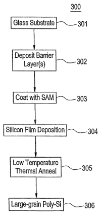
[00036] Fig. 3 is a flow chart of an illustrative
processing sequence 300 for fabricating a display device
such as display 100 according to an exemplary embodiment.
It is noted that the processing sequence,.materials and
process parameters, in many instances, are substantially
the same as the description of the processes of the
exemplary embodiments described in connection with. Figs.
2a-2e above. To the extent that these are applicable to
the process of the exemplary embodiment of Fig. 3, these
are not repeated.
[00037] The glass substrate is provided at 301, and a
barrier layer is disposed thereover at step 302. The
barrier layer is used to block migration of contaminants
from the substrate into the device region. The barrier
layer commonly consists of silicon nitride, silicon
dioxide, or a combination of the two, and is typically
deposited by chemical vapor deposition (CVD) to a
thickness of 100 to 500 nm. After the disposition of the
CA 02532638 2006-O1-16
WO 2005/010964 PCT/US2004/019946
barrier layer, the SAM material is deposited over the
substrate at step 303. After the SAM deposition, the
silicon layer is deposited at step 304. This is followed
by a relatively low-temperature thermal anneal step 305,
which substantially eliminates any amorphous silicon,
forming the crystalline silicon instead, and pyroli~es the
SAM layer. This results in the formation of substantially
large grain polysilicon or monocrystalline silicon on the
surface of the substrate at step 306.
(00038] The invention having been described in detail in
connection through a discussion of exemplary embodiments,
it is Clear that modifications of the invention will be
apparent to one having ordinary skill in the art having
had the benefit of the present disclosure. Such
modifications and variations are included in the scope of
the appended claims.