Note: Descriptions are shown in the official language in which they were submitted.
CA 02532771 2012-10-29
HIGH-FREQUENCY POWER TRANSFORMER
Field
[0001] This invention relates to power transformers. In particular, this
invention
relates to the integration and connection of a power stage to a high-
frequency, high-current power
transformer in a switch mode power supply.
Background
[0002] A power stage of a voltage step-up switch mode power supply ("SMPS")
drives the primary (low voltage) winding of a transformer with a high
frequency alternating
voltage, creating an alternating magnetic field around the primary winding and
through a core of
the transformer. One or more secondary (high voltage) windings are also
wrapped around the
core and are located in close proximity to the primary winding. The
alternating magnetic field
around the primary winding induces an AC voltage in the secondary winding. In
most SMPS,
the AC output of the transformer's secondary winding is rectified to provide a
DC voltage at the
output of the power supply. Compared with a low-frequency power supply, a high-
frequency
SMPS has a number of advantages, the most significant of which are suitability
for low-cost
manufacturing, and reduced size and weight. Consequently, SMPSs are considered
to be more
economical than low-frequency power supplies. With a voltage step-down SMPS
the process
occurs in reverse, with the primary winding being the high voltage winding and
the secondary
winding being the low voltage winding.
[0003] Surface mounted active and passive electronic components, commonly
called
surface mounted devices ("SMDs"), are typically employed in SMPS applications
to further
1
v.2
CA 02532771 2006-01-11
reduce the size and weight of the power supply. SMDs are also well-suited for
automated and
high-volume production, making them more cost-effective than non-surface
mounted designs. In
order to reduce the size of SMDs and thus further reduce the size and weight
of the SMPS, it is
necessary to increase the commutation frequency of the power devices in the
power stage of the
SMPS. When the commutation frequency is increased, the length of connecting
wires
conducting high frequency current between the power stage and the transformer
are preferably
minimized in order to eliminate parasitic impedances, which can reduce the
efficiency of SMPS
and generate electromagnetic interference ("EMI"). Parasitic impedances can be
a significant
issue with high-frequency SMPS where the high-frequency currents, e.g.,
typically in the range of
about 100-200 kHz, often reach around 300 to 400 amperes in low-voltage
circuits, e.g., in the
range of about 10-60 volts RMS, of the SMPS. Losses and impedances in the
connecting wires
can be significant enough that it becomes unacceptably inefficient or
impractical to use a high
commutation frequency, thereby forcing SMPS designers to resort to lower
frequencies, e.g.,
around 50 kHz, with the corresponding size and weight disadvantages.
[00041 There is a need for a cost-effective way to reduce parasitic impedances
associated with connecting wires in high-frequency, high-current switch mode
power supplies,
this parameter being critical to good performance.
Summary
[00051 According to the present invention, the usual connecting wires between
a low
voltage power stage and a transformer of a SMPS are replaced with bus bars
that are incorporated
into and made part of a power transformer magnetic system. The low voltage,
high-current
windings of the power transformer also serve as an integral bus bar,
connecting the power
transformer with a power stage comprised of power switching devices such as
metal oxide
2
v.2
CA 02532771 2006-01-11
semiconductor field effect transistors ("MOSFETs"). The low voltage power
stage can be
configured as either an H-bridge or a half bridge.
An aspect of the present invention is a high-frequency transformer. The
transformer
comprises a high-voltage winding. A first bus bar is positioned proximate the
high voltage
winding and extends to a first portion of a plurality of power switching
devices. The first bus bar
is electrically coupled to the first portion of the power switching devices. A
second bus bar is
positioned proximate the high voltage winding and extends to a second portion
of the power
switching devices. The second bus bar is electrically coupled to both the high
voltage winding
and the second portion of the power switching devices. A third bus bar extends
between the first
and second bus bars and is electrically coupled to the first bus bar, second
bus bar, and the high
voltage winding. The second and third bus bars form a low voltage winding that
electrically
cooperates with the high voltage winding to form the high-frequency
transformer.
Brief Description of the Drawings
[0006] Further features of the inventive embodiments will become apparent to
those
skilled in the art to which the embodiments relate from reading the
specification and claims with
reference to the accompanying drawings, in which:
[0007] Fig. 1 depicts a perspective view of a power supply board for a switch
mode
power supply, comprising a low-voltage power stage and a transformer according
to an
embodiment of the present invention;
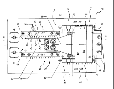
[0008] Fig. 2 is a top plan view of the power supply board of Fig. 1;
[0009] Fig. 3 is a side elevational view of the power supply board of Fig. 1;
[0010] Fig. 4 is an end elevational view of the power supply board of Fig. 1;
3
v.2
CA 02532771 2006-01-11
[0011] Fig. 5 is a schematic diagram of a portion of a power supply according
to an
embodiment of the present invention;
[0012] Fig. 6 is an elevational view of a power supply board for a switch mode
power
supply wherein the transformer (shown without a core for clarity) includes a
coaxial bus bar
according to an embodiment of the present invention;
[0013] Fig. 7 is a first side elevational view of a power supply board for a
switch
mode power supply, comprising a power stage and a coreless transformer
according to an
alternate embodiment of the present invention; and
[0014] Fig. 8 is a view in section (8-8) of the power supply board of Fig. 2.
Detailed Description
[0015] In the discussion that follows, like reference numerals will be used to
represent like structures in the various embodiments. A low voltage printed
circuit board
assembly ("PSA") 10, shown in Figs. 1-4, includes an assembled power
transformer 12. PSA 10
further includes a power stage arranged as an H-bridge power switch 14 with
commutation
frequency of about 200 kHz. In other embodiments, other frequencies and power
switch
arrangements may be used, such as a half-bridge configuration. Current flowing
through a low
voltage winding of the power transformer of the embodiment shown may be in the
range of up to
about 350 amperes RMS continuously. PSA 10 is assembled upon a printed circuit
board 18
using a plurality of SMD components 20, as discussed in more detail below, to
make up power
switch 14. In the embodiment shown, PSA 10 is a subassembly of a bi-
directional DC-DC
converter and may be configured with a voltage ratio of about 40 to 1.
[0016] Power transformer 12 may include a ferrite core assembly 22 comprising
three
U-shaped cores 24 and three I-shaped cores 26. The number of cores 24, 26 may
vary, depending
4
v.2
CA 02532771 2006-01-11
upon the operating voltage for a particular power transformer 12 and the
selected commutation
frequency. The low voltage winding of transformer 12 may be one turn located
proximate a high
voltage winding 27 of the power transformer and inductively electrically
coupled thereto. One
example embodiment of the present invention utilizes a first bus bar 30, a
second bus bar 32 and
a third bus bar 38. In the example embodiment, as shown in Fig. 2, a single-
turn low-voltage
winding is comprised of second bus bar 32 and third bus bar 38. Transformer 12
also includes a
pair of electrical connection terminals 28, coupled to the high voltage
winding 27.
[0017] First bus bar 30 connects a source terminal of each of a first group 40
of
power devices such as MOSFETs, identified as Q1-Q7 in Fig. 2, with a drain
terminal of a
second group 42 of MOSFETs, identified as Q8-Q14 in Fig. 2, to form a first
leg of power stage
14. Likewise, second bus bar 32 connects the source terminals of a third group
44 of MOSFETs,
identified as Q15-Q21 in Fig. 2, with the drain terminals of a fourth group 46
of MOSFETs,
identified as Q22-Q28 in Fig. 2, to form a second leg of power stage 14. The
width of bus bar 32
is generally equal to the width of a core window 34 of power transformer 12,
shown best in Fig.
4, to minimize losses and maximize performance. Bus bar 32 also provides a
first portion of the
low voltage turn of transformer 12, extending generally from "Cl" to "C2." A
plurality of
decoupling capacitors 48 may be located underneath the bus bars 30, 32. The
capacitors serve to
provide a low impedance supply to an H-bridge formed in a conventional manner
by MOSFET
groups 40, 42, 44, 46 (Q1-Q28). The width of bus bar 30 is determined by the
space needed by
capacitors 48, located under the bus bar, by the requirement to handle the
full transformer low
-voltage winding current, and the need to minimize parasitic inductance.
Similarly, the length and
shape of bus bar 30 is determined by the physical size, locations and number
of MOSFETs. A
plurality of vents 36 may be disposed in bus bars 30, 32 to promote air
circulation, and allow
v.2
CA 02532771 2012-10-29
soldering of the components during assembly. A schematic diagram showing the
general
electrical arrangement of MOSFETs 40, 42, 44, 46, capacitors 48 and bus bars
32, 38 is shown in
Fig. 5.
[0018] A third bus bar 38, shown in Figs. 1-5, provides an electrical
connection
between bus bar 30 and bus bar 32. Bus bar 38 extends through core window 34
and has a width
that is generally equal to the width of the core window. Bus bar 38 provides a
second portion of
the low voltage winding, extending generally from "C2" to "Cl" and extending
down to bus bar
32, minimizing leakage inductance. Thus, taken together, bus bars 32 and 38
form one complete
turn of a low voltage winding of the power transformer electrically coupled to
high voltage
winding 27.
[0019] Electrical current flows in bus bar 32 and bus bar 38 in opposite
directions,
flowing generally between "Al" and "A2." Thus, the gap between bus bar 32 and
bus bar 38
between "Al" and "A2" is preferably small. The gap may be controlled in any
conventional
manner including, without limitation, tape, spacers and insulators. The
minimal gap partially
compensates for the inductance of bus bars 32, 38 between "Al" and "A2."
[0020] A particular advantage of the present invention is reduction of leakage
inductance associated with power transformer 12 and its terminations. As noted
above, this is
accomplished by minimizing the distance between MOSFETs 40, 42, 44, 46 and
power
transformer 12, as shown in Figs. 1-4.
[0021] In another embodiment of the present invention, shown in Fig. 6, a
power
supply 10' has a transformer 12' wherein a bus bar 38' is formed into a
coaxial shape with the
addition of coaxial elements 39. Coaxial elements 39 are each electrically
coupled to bus bar 38'
at both edges of the bus bar and encircle a high voltage winding 27'. In this
embodiment the
6
v.2
CA 02532771 2012-10-29
leakage inductance becomes even smaller, reaching values for the transformer
as low as about 10
nH and having low external fields. In addition, inductive coupling between the
low
voltage and high voltage windings of transformer 12' is increased.
[0022] Although only two coaxial elements 39 are shown in Fig. 6, one skilled
in the
art will recognize that electrical connection terminal 28 may be re-shaped
and/or relocated, such
as to a corner of high voltage winding 27', to facilitate additional coaxial
elements, each element
encircling high voltage winding 27' and being electrically connected to bus
bar 32' in the manner
previously described. In the embodiment of Fig. 6, for example, as many as
four coaxial
elements 39 may be coupled to bus bars 32' and 38, each coaxial element 39
encircling the
generally rectangular-shaped high voltage winding 27' at each of the winding's
four generally
planar inner surfaces.
[0023] Figs. 7 and 8 depict a power supply board 10" having a coreless
transformer
12". Coreless transformer 12" is usable at higher switching frequencies where
less magnetizing
inductance is required as compared to lower switching frequencies. The
foregoing discussion for
power supply board 10 is equally applicable to power supply board 10" and thus
will not be
reiterated herein.
[00241 In some embodiments of the present invention bus bar 30 has the same
general
shape and dimensions as bus bar 32, providing for minimal leakage inductance
by locating the
bus bars closer together. This embodiment eliminates the need for tapering bus
bar 38.
[0025] The transformers of present invention, described above, may be
configured for
use in a bidirectional DC-DC converter. Accordingly, the low voltage winding
formed by the
second and third bus bars may function as either a primary winding for a step-
up converter or a
secondary winding for a step-down converter. Likewise, the high voltage
winding may function
7
v.2
CA 02532771 2006-01-11
as either a secondary winding for a step-up converter or a primary winding for
a step-down
converter. The transformers described herein are not limited to DC-DC
converters, and may also
be utilized with AC-DC, DC-AC and AC-AC converters for voltage step-up,
voltage step-down,
or electrical isolation without a change in voltage level.
[00261 While this invention has been shown and described with respect to a
detailed
embodiment thereof, it will be understood by those skilled in the art that
changes in form and
detail thereof may be made without departing from the scope of the claims of
the invention.
8
v.2