Note: Descriptions are shown in the official language in which they were submitted.
CA 02532864 2006-O1-16
WO 2005/059952 PCT/US2004/024290
LANGMUIR-BLODGETT NANOSTRUCTURE MONOLAYERS
CROSS-REFERENCE TO RELATED APPLICATIONS
[0001] This application claims priority from U.S. provisional application
serial
number 60/490,975 filed on July 28, 2003, incorporated by reference in its
entirety.
STATEMENT REGARDING FEDERALLY SPONSORED RESEARCH
OR DEVELOPMENT
[0002] Not Applicable
INCORPORATION-BY-REFERENCE OF MATERIAL
SUBMITTED ON A COMPACT DISC
[0003] Not Applicable
NOTICE OF MATERIAL SUBJECT TO COPYRIGHT PROTECTION
[0004] A portion of the material in this patent document is subject to
copyright
protection under the copyright laws of the United States and of other
countries. The owner of the copyright rights has no objection to the facsimile
2o reproduction by anyone of the patent document or the patent disclosure, as
it
appears in the United States Patent and Trademark Office publicly available
file or records, but otherwise reserves all copyright rights whatsoever. The
copyright owner does not hereby waive any of its rights to have this patent
document maintained in secrecy, including without limitation its rights
pursuant
to 37 C.F.R. ~ 1.14.
BACKGROUND OF THE INVENTION
1. Field of the Invention
[0005] This invention pertains generally to the organization of anisotropic
so building blocks into functional nanoscale assemblies with high packing
density, and more particularly to formation of monolayers of nanostructures
using the Langmuir-Blodgett technique and devices and mechanisms
-1-
CA 02532864 2006-O1-16
WO 2005/059952 PCT/US2004/024290
fabricated therefrom.
2. Description of Related Art
[0006] Techniques for directing the assembly of metal or semiconductor
quantum dots into superstructures have been pursued over the years. Few
studies have addressed the organization of one-dimensional nanoscale
building blocks such as nanotubes, nanowires, and nanorods into ordered
structures except for the 3-dimensional spontaneous superlattice formation of
nanorods made from certain materials. On the other hand, Kim, F. et al.,
"Langmuir-Blodgett Nanorod Assembly", J. Am. Chem. Soc. 123, 4386-4389
o (2001 ), incorporated herein by reference, describes a method for
fabricating a
2-dimensional monolayer assembly of BaCr04 nanorods using the Langmuir-
Blodgett technique.
[0007] Various researchers have successfully prepared Langmuir-Blodgett
films of spherical nanoparticles such as Ag, Au, and CdS. Typically, the
~s surface of the nanocrystals are functionalized by organic molecules
(usually
long alkyl chains) in order to prevent particle aggregation and also to ensure
the floating of the nanoparticles on the subphase surface (usually water). The
nanoparticles are then dispersed in organic solvents such as toluene, and this
solution is spread drop-wise onto the subphase surface. The nanoparticles
2o form a monolayer on the water-air interface, which is slowly compressed.
This
monolayer can be transferred during the compression using either horizontal
or vertical liftoff to substrates such as TEM grid or Si wafer to be inspected
under electron and optical microscopes. For spherical nanoparticles, the
particles form a gas phase at low densities, where the monolayer is highly
25 compressible without significant increase in the surface pressure.
Depending
on the particle size, the length of the capping ligand, and the surface
pressure, various microscopic structure of islands, wires, and rings composed
of the nanoparticles can be formed. As the monolayer is compressed, the
nanoparticles start to form a condensed phase, usually a hexagonally close
3o packed structure due to the isotropic inter-particle interactions.
[0008] Nanoscale science, however, is about assembling matter at multiple
length scales, from atomic and molecular species to individual nanoscale
-2-
CA 02532864 2006-O1-16
WO 2005/059952 PCT/US2004/024290
building blocks such as nanocrystals, nanorods and nanowires, then from
these individual nanoscale building blocks to higher-level functional
assemblies and systems. This hierarchical process covers length scale of
several orders, from A to micrometer or larger. The past decades have
witnessed great progress in the direction of synthesizing nanocrystals of
various compositions and sizes. Significant progress has been made in the
area of nanowire synthesis and device application. Successful alignment and
patterning of nanowires would significantly impact many areas such as
nanoscale electronics, optoelectronics and molecular sensing. A grand
~o challenge, however, resides in the hierarchical integration of the
nanoscale
building blocks into functional assemblies and ultimately to a system.
[0009] Unlike the traditional lithographical process where precise placement
of
certain elements or devices is embedded in the designing process, the
precise placement of nanoscale building blocks on the right place with right
configuration and with exceedingly high densities represents a daunting task
for researchers in this field.
[0010] Nanoparticles have attracted a great deal of attentiori due to their
potential applications in optics, electronics, and catalysis. Different
methods
have been developed to synthesize metallic and semiconductor nanoparticles
20 of different sizes. In the synthesis of new materials based on an ordered
assembly of nanoparticles, three significant factors are important in
determining the interactions between the nanoparticles and ultimately their
superstructures, namely the shape and size distributions of the nanoparticles,
and the surface functionality of the nanoparficles. A major motivation for
25 research in this field remains the challenge to understand how ordered or
complex structures form by self- or directed-assembly, and how such
processes can be monitored/controlled in order to prepare structures with a
pre-determined geometry/superstructure.
[0011] A prerequisite for nanostructure preparation via the assembly route is
so the availability of sufficiently stable building blocks that are highly
uniform in
size and shape. Techniques for directing the assembly of metal or
semiconductor quantum dots into novel superstructures have been
-3-
CA 02532864 2006-O1-16
WO 2005/059952 PCT/US2004/024290
extensively pursued over the past decades. Impressive accomplishments in
the area of self-assembly of metallic silver and gold nanoparticles,
semiconductor CdSe and Ag2S quantum dots and spherical nanoparticles
have been reported. This is due to the possibility of obtaining these
spherical
nanoparticles as highly monodispersed and stable products. In spite of the
large volume of research on the self-assembly of quantum dots, however, little
attention has been devoted to the self-assembly of rod-shaped nanoparticles
(nanorods) and particles with other different shapes (prisms, hexagons,
cubes). This is partly due to the fact that there is no chemistry available
for
o preparing these highly uniform facetted nanocrystals.
[0012] After decades of research, the size control of the metal and
semiconductor nanocrystals is now well-established. The deterministic shape
control is, however, still in its infancy although recent efforts into nanorod
synthesis have resulted in some very exciting progress. In addition, there has
been progress toward shape control of II-IV compound nanocrystals, where
easy axis (6-fold symmetry) exists within the crystal structure and has
profound impact on the resulting nanocrystal growth habits. In general,
however, the mechanism of shaped nanocrystal growth, particularly for those
metal systems, is still much elusive and currently under hot debate.
[0013] Nanocrystal shape control is still a highly empirical process due to
the
lack of fundamental understanding of the complex growth process with
multiple synthetic parameters. One known approach to shape control is to
use surfactants during the metal reduction and particle growth. The surfactant
has a role to control the crystal shapes by attaching to selected crystal
surface
during the growth. Of course, the surfactants also stabilize the metal
particles
and avoid the undesirable aggregation. In this regard, some linear polymers
are recently found to be highly effective to control the crystal shapes. For
example, polyacrylate, poly-(N-vinyl-2-pyrrolidone) and polyvinyl alcohol have
been used to control the metal particle shapes with a reasonable yield. A
so main advantage of this surfactant/polymer approach for shaped crystal
synthesis is the relative large yield and its potential to produce high purity
products.
-4-
CA 02532864 2006-O1-16
WO 2005/059952 PCT/US2004/024290
[0014] Besides the surfactant approach, one additional important factor that
could determine the final crystal shapes is the addition of foreign ions. For
example, it has been found that different ions and ionic strength could be
used to modulate the copper nanocrystal shapes. It has also been found that
a small amount of silver addition is critical for the formation of gold
nanorods
in an electrochemical process.
[0015] Therefore, there is a need for a method of assembling monolayers of
nanostructures other than spherical nanoparticles. There is also a need for a
method of controlling shape synthesis of metal nanostructures and mediating
o the interaction among these particles to form different 2-dimensional (2D)
or
3-dimensional (3D) superstructures. The resultant superstructures are of
importance for their tunable collective physical properties (e.g. optical,
magnetic and catalytic properties), where inter-object separation, shape and
interfacial structure enable the tuning of properties.
BRIEF SUMMARY OF THE INVENTION
[0016] The present invention addresses the foregoing needs by adapting the
Langmuir-Blodgett (LB) technique for assembly of monolayers of
nanostructures other than spherical nanoparticles. Surface functionalization
of these nanostructures is used to mediate the interaction among these
2o particles to form different 2-dimensional (2D) or 3-dimensional (3D)
superstructures.
[0017] In one beneficial embodiment of the invention, a method for fabricating
a monolayer of nanostructures comprises the steps of forming a plurality of
nanostructures, rendering the nanostructures hydrophobic, dispersing the
hydrophobic nanostructures onto a water surface of a Langmuir-Blodgett
trough and forming a monolayer film of ordered nanostructures, and
compressing the monolayer film. In a further embodiment, the shape of the
nanostructures is controlled and selected from the group consisting
essentially
of cube-shaped, plate-shaped, rod-shaped, triangle-shaped, and hexagon-
3o shaped.
[0018] In another beneficial embodiment of the invention, a method for
fabricating monolayer of silver nanowires comprises forming silver nanowires
-5-
CA 02532864 2006-O1-16
WO 2005/059952 PCT/US2004/024290
using a solution-phase polyol process wherein said nanowires have faceted
cross-sections, rendering the nanowires hydrophobic, dispersing the
hydrophobic nanowires onto a water surface of a Langmuir-Blodgett trough
and forming a monolayer film of nanowires that exhibit substantial parallel
s alignment, and compressing the monolayer nanowire film and forming a
monolayer through an insulator-to-metal transition.
[0019] In the case of the formation of silver nanowires, the diameters of
approximately 50 nm are achievable. The nanowires can have various cross-
sectional shapes, including pentagonal cross-sections, and the tips can be
o pyramidal with vertices as sharp as 2 nm. The nanowires can be formed as
close-packed as parallel arrays with their longitudinal axes aligned
perpendicular to the compression direction.
[0020] In the foregoing embodiments, the area of the compressed monolayer
film can vary to as much as 20 cm2 or greater, and the monolayer film
15 beneficially can be deposited onto a substrate for support and structure
formation. The substrate can be selected from various materials such as
silicon wafers, glass slides, and polymer and other substrates.
[0021] The monolayer is capable of functioning as a surface enhanced Raman
Spectroscopy (SERS) substrate for molecular sensing, and is suitable for
2o molecular-specific sensing utilizing vibrational signatures. Optionally,
the
monolayer can be configured for the detection of 2,4-dinitrotoluene (2,4-
DENT), for use as an interconnect, as a component in a multilayer structure.
[0022] Optionally, the monolayer can be embedded in polydimethylsiloxane
(PDMS), in which case the embedded monolayer is capable of functioning as
2s a simple wire-grid optical polarizer.
[0023] An aspect of the present invention is assembly of monolayers of
aligned silver nanowires using the Langmuir-Blodgett technique. In one
embodiment, the monolayers have an area over 20 cm2. In one embodiment
the nanowires are ~ 50 nm in diameter. In one embodiment, the nanowires
so possess pentagonal cross-sections. In one embodiment, the nanowires
possess pyramidal tips. In one embodiment the pyramidal tips have vertices
as sharp as 2 nm.
-6-
CA 02532864 2006-O1-16
WO 2005/059952 PCT/US2004/024290
[0024] Another aspect of the invention is assembly of monolayers of aligned
silver nanowires which are close-packed and aligned parallel to each other
using the Langmuir-Blodgett technique.
[0025] A further aspect of the invention is assembly of monolayers of aligned
silver nanowires which are close-packed as parallel arrays with their
longitudinal axes aligned perpendicular to the compression direction.
[0026] Another aspect of the invention is assembly of monolayers of aligned
silver nanowires that serve as surface enhanced Raman Spectroscopy
substrates.
o [0027] Another aspect of the invention is assembly of monolayers of aligned
silver nanowires that are suitable for molecular-specific sensing utilizing
vibrational signatures.
[0028] Another aspect of the invention is to embed monolayers of silver
nanowires within polydimethylsiloxane (PDMS).
[0029] Another aspect of the invention is to embed multilayers of silver
nanowires within polydimethylsiloxane (PDMS).
[0030] Another aspect of the invention is to form flexible nanowire-polymer
composites that can serve as simple wire-grid optical polarizers.
[0031] Another aspect of the invention is to provide monolayer structures
2o suitable for chemical and biological sensing.
[0032] According to a further aspect of the invention, aligned silver nanowire
monolayers can be readily used as surface-enhanced Raman spectroscopy
(SERS) substrates for molecular sensing. In one embodiment, an aligned
silver nanowire monolayer is configured for the detection of 2,4-
dinitrotoluene
(2,4-DENT).
[0033] Note that the use of the use of our inventive nanowire monolayer as
SERS substrates has several advantages. First, the surface properties of
these nanowire monolayer are highly reproducible and well-defined as
compared to other systems. Second, several unique features of the
so nanowires, such as sharp vertices, non-circular pentagonal cross-sections,
inter-wire coupling, may lead to larger field enhancement factors, offering
higher sensitivity under optimal conditions. In addition, strong wire coupling
-7-
CA 02532864 2006-O1-16
WO 2005/059952 PCT/US2004/024290
within the monolayer enables SERS experiments with a broad selection of
excitation sources. Lastly, these monolayers can readily be used for molecular
detection in either an air-borne or a solution environment. Hence, nanowire-
based sensors using our inventive monolayer could have significant
implications in chemical and biological warfare detection, national and global
security, as well as medical detection applications.
[0034] Accordingly, another aspect of the invention comprises high density
nanoscale interconnects, sensor arrays, and multilayer structures.
[0035] Another aspect of the invention is to transfer monolayers according to
o the present invention to any desired substrates, including silicon wafers,
glass
slides, and polymer substrates.
[0036] A still further aspect of the invention is to form 2-dimensional
superstructures from shape controlled nanocrystals and nanowires using the
Langmuir-Blodgett technique.
s [0037] Another aspect of the invention is to assemble cube-shaped, plate-
shaped, rod-shaped, triangle-shaped, and hexagon-shaped nanocrystals into
2-dimensional superstructures using the Langmuir-Blodgett technique.
[0038] Another aspect of the invention is to form monolayer structures that
can
be used in lithography applications.
20 [0039] Further aspects of the invention will be brought out in the
following
portions of the specification, wherein the detailed description is for the
purpose of fully disclosing preferred embodiments of the invention without
placing limitations thereon.
BRIEF DESCRIPTION OF THE SEVERAL VIEWS
25 OF THE DRAWINGS)
[0040] The invention will be more fully understood by reference to the
following drawings which are for illustrative purposes only:
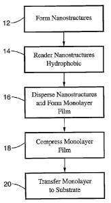
[0041] FIG. 1 is a flow diagram of an embodiment of a monolayer assembly
process according to the present invention.
30 [0042] FIG. 2A and B are transmission electron microscopy images of uniform
Ag nanowires employed in an embodiment of the assembly process according
to the present invention. The inset in FIG. 2A is an image taken from a
_8_
CA 02532864 2006-O1-16
WO 2005/059952 PCT/US2004/024290
microtomed sample, showing the pentagonal cross-sections of the nanowires.
A high resolution TEM image, the upper inset in FIG. 2B, shows the sharp
pentagonal pyramidal tip of a silver nanowire, as schematically illustrated in
the bottom inset in FIG. 2B.
[0043] FIG. 3A through C are photographs showing the Langmuir-Blodgett
(LB) nanowire assembly process of the present invention at different
progressive compression stages.
[0044] FIG. 4 is a surface pressure curve recorded during the assembly
process illustrated in FIG. 3.
o ' [0045] FIG. 5A through D are scanning electron microscopy images (at
different magnifications) of the silver nanowire monolayer deposited on a
silicon wafer according to an embodiment of the present invention.
[0046] FIG. 6 illustrates the UV-VIS absorption spectra of a silver nanowire
monolayer assembled according to an embodiment of the present invention.
All spectra were obtained at normal incidence with the polarization angles (P)
defined as 8 = 0°, when the incident electric field is parallel to the
direction of
nanowire alignment and 8 = 90° when the filed is perpendicular to the
nanowire axis.
[0047] FIG. 7 is a graph illustrating surface-enhanced Raman spectroscopy on
2o a silver nanowire monolayer assembled according to an embodiment of the
invention, showing SERS spectra of 1-hexadecanethiol on a Langmuir-
Blodgett film of silver nanowires with visible (532 nm, 25 mW) and near-
infrared excitation (785 nm, 10 mW).
[0048] FIG. 8 is a graph illustrating surface-enhanced Raman spectroscopy on
2s a silver nanowire monolayer assembled according to an embodiment of the
invention, showing SERS spectrum of R6G on the thiol-capped Ag-LB film
(532 nm, 25 mW) after 10 min incubation in a 10-9 M R6G solution. The inset
shows the linear relationship between the Raman intensity (ISERS, ~sso) and
the
R6G concentration.
30 [0049] FIG. 9 is a graph illustrating surface-enhanced Raman spectroscopy
on
a silver nanowire monolayer assembled according to an embodiment of the
invention, showing SERS spectrum of 2,4-DNT on the thiol-capped Ag
_g_
CA 02532864 2006-O1-16
WO 2005/059952 PCT/US2004/024290
nanowire monolayers after incubation for 10 min in 10-2 M 2,4-DNT/MeOH
solution. The spectrum was recorded using 25 mW of 532 nm laser light. The
acquisition time was 10 s.
[0050] FIG. 10A and B are optical images of a silver nanowire monolayer
assembled according to an embodiment of the invention under cross-
polarizer. The imaging area corresponds to 735 by 521 ,um.
[0051] FIG. 11 illustrates the UV-VIS spectrum of five photochemically
prepared gold nanorod solutions according to an embodiment of the invention
where solution A was prepared with no silver ion addition, and solutions B-E
1o were prepared with increasing amount of silver nitrate solution.
[0052] FIG. 12A-C are transmission electron microscopy (TEM) images of gold
nanorods prepared with increasing amounts of silver nitrate solution addition
according to an embodiment of the invention, where the bar in the lower
portion of each image indicates 50 nm.
15 [0053] FIG. 13 is a high resolution image of a gold nanorod shown in FIG.
12.
[0054] FIG. 14A-D are transmission electron microscopy images of nanorod
assemblies at water/air interface at different stages of the compression
according to an embodiment of the invention, where FIG. 14A shows isotropic
distribution at low pressure, FIG. 14B is monolayer with nematic arrangement,
2o FIG. 14C is a monolayer with smectic arrangement, and FIG. 14D is a
nanorod multilayer with nematic configuration, and where the insets in FIG.
14B and FIG. 14D are the Fourier transform of the corresponding image.
[0055] FIG. 15A-E are schematic diagrams showing the organization of
shaped nanocrystals according to an embodiment of the invention.
25 [0056] FIG. 16A-E are images of shaped nanostructures according to the
present invention, wherein FIG. 16A and B are TEM images of truncated
tetrahedral gold nanoparticles and the inset in FIG. 16B is the electron
diffraction pattern taken along the [111] zone axis from the particle shown in
FIG. 16B, and FIG. 16C and D are SEM images of several partially developed
so gold tetrahedra.
[0057] FIG. 17A-B are images of icosahedral nanocrystals according to the
present invention wherein FIG. 18A is a TEM image and FIG. 17B is a SEM
-10-
CA 02532864 2006-O1-16
WO 2005/059952 PCT/US2004/024290
image of icosahedral gold nanoparticles, and wherein the inset in FIG. 17B
shows clearly all X111} facets of a typical icosahedron.
[0058] FIG. 18A-C are TEM and SEM images of some minority particles
observed during synthesis according to the present invention wherein FIG.
s 18A and B shown decahedrons and FIG. 18C shows an octahedron.
[0059] FIG. 19A-D are TEM and SEM images of gold nanocubes according to
the present invention dispersed on a TEM grid and a silicon substrate wherein
the inset in FIG. 19C shows the electron diffraction pattern recorded along
the
[100] zone axis of a gold nanocube shown in FIG. 19D.
[0060] FIG. 20 shows the X-ray diffraction patterns for the three types of
gold
nanocrystals according to the present invention: tetrahedron, cube and
icosahedron.
[0061] FIG. 21 shows the UV-VIS spectra for the three types of gold
nanocrystals: tetrahedron, cube and icosahedron of FIG. 20.
[0062] FIG. 22A-C are images of Pt cubes according to the present invention,
wherein FIG. 22A is a TEM image of Pt cubes, FIG. 22B is an HRTEM image
of the Pt cube along the [001] zone axis, and FIG. 22C is an HRTEM image of
the Pt tetrahedron along the [111] zone axis.
[0063] FIG. 23A-C are images of cuboctahedra according to the present
2o invention, wherein FIG. 23A is a TEM image of Pt cuboctahedra, FIG. 23B is
an HRTEM image of the Pt cuboctahedron along the [110] zone axis, and
FIG. 23C is a 2D projection of an ideal cuboctahedron along the [110]
direction.
[0064] FIG. 24A-C is are images of Pt octahedra according to the invention
wherein FIG 24A is a TEM image of Pt octahedral, FIG. 24B is an HRTEM
image of the Pt octahedron along the [110] zone axis, and FIG. 24C is an
HRTEM image of the Pt octahedron along the [001] zone axis.
[0065] FIG. 25 is a flow diagram illustrating a generalization of the modified
polyol process according to the invention.
3o DETAILED DESCRIPTION OF THE INVENTION
[0066] The present invention generally comprises methods for fabricating a
monolayer of nanostructures and assemblies and devices therefrom. By way
-11-
CA 02532864 2006-O1-16
WO 2005/059952 PCT/US2004/024290
of example, and not of limitation, an embodiment of the fabrication method is
illustrated in FIG. 1. In the exemplary embodiment shown in FIG. 1, a
plurality
of nanostructures is formed a step 12. After the nanostructures are formed,
they are rendered hydrophobic at step 14. At step 16, the nanostructures are
s then dispersed onto a water surface of a Langmuir-Blodgett (LB) trough and a
monolayer of ordered nanostructures is formed. The monolayer is then
compressed at step 18, and transferred to a substrate at step 20.
[0067 It will be appreciated that, during the formation step 12, the
nanostructures can be formed with various lengths and cross-sectional
1o shapes. The resultant nanostructures can have shapes that include, but are
not limited to, cubic, plate-shaped, rod-shaped, triangular, pentagonal and
hexagonal. In one beneficial embodiment for use as sensors, the
nanostructures can be nanowires having diameters of up to approximately 50
nm and pyramidal tips with vertices as sharp as 2 nm. The size of the
15 monolayer can be varied, and areas exceeding approximately 20 cm2 are
achievable. The transfer step 20 can comprise, for example, depositing the
compressed monolayer onto the surface of a substrate such as silicon, glass,
polymer or other material, or embedding the monolayer into a polymer
material such as polydimethylsiloxane (PDMS). The resultant monolayers are
2o suitable for use in surface enhanced Raman spectroscopy (SERS), for
molecular-specific sensing using vibrational signatures, as interconnects, and
as wire-grid optical polarizers. Assemblies and devices can be formed by
placing the monolayer into multilayer structures.
[0068] In another beneficial embodiment, the nanostructures are silver
25 nanowires formed using a solution-phase polyol process wherein the
nanowires have faceted cross-sections. In this embodiment, a monolayer film
is formed in step 16 where the nanowires exhibit substantial parallel
alignment. During the compression step 18 the monolayer is formed through
an insulator-to-metal transition. nanowires are close-packed as parallel
arrays
3o with their longitudinal axes aligned perpendicular to the compression
direction.
[0069] EXAMPLE 1
[0070] In the following discussion, we report our success with utilizing the
-12-
CA 02532864 2006-O1-16
WO 2005/059952 PCT/US2004/024290
foregoing processes to assemble aligned monolayers (with area over 20 cm2)
of silver nanowires that are ~50 nm in diameter and 2-3 micrometers in length.
These nanowires (characterized by pentagonal cross-sections and pyramidal
tips) were close-packed as parallel arrays, with their longitudinal axes
aligned
perpendicular to the compression direction. The resulting nanowire
monolayers can serve as good surface enhanced Raman Spectroscopy
substrates, exhibit large electromagnetic field enhancement factors (2x10⁵ for
thiol and 2,4-dinitrotoluene, 2x10⁹ for Rhodamine 6G) and can readily be used
in ultrasensitive, molecular-specific sensing utilizing vibrational
signatures.
[0075] Silver nanowires were prepared using polyvinyl pyrrolidone) (PVP) as
the capping agent. The as-prepared samples were purified to remove
spherical nanoparticles. The resulting nanowires were uniform in both
diameter (45.3~3.6 nm) and aspect ratio (45~5). After functionalizing with
1-hexadecanethiol ligands, the wires were rendered hydrophobic and re-
dispersed in chloroform. FIG. 2A and B are transmission electron microscopy
images of the uniform Ag nanowires before the LB assembly. The inset in
FIG. 2A is an image taken from a microtomed sample, showing the
pentagonal cross-sections of the nanowires. A high resolution TEM image,
the upper inset in FIG. 2B, shows the sharp pentagonal pyramidal tip of a
2o silver nanowire, as schematically illustrated in the bottom inset in FIG.
2B. An
important feature of these nanowires was their pentagonal cross-sections, as
shown in the inset of FIG. 2A. In addition, these wires possessed pentagonal
pyramidal ends with vertices as sharp as 2 nm as shown in the lower inset of
FIG. 2B. The non-circular cross-sections and sharp wire tips potentially have
important corisequence for molecular sensing using surface enhanced Raman
spectroscopy (SERS).
[0079] The nanowires were then dispersed onto a water surface of the
Langmuir-Blodgett trough. It is important to note that the displacement of the
PVP capping agents with thiol ligands was required to render the nanowire
so surface hydrophobic as well as to prevent aggregation.
[0080] The assembly process was effectively a microscopic version of "logs-
on-a-river". FIG. 3A through C are photographs showing the LB nanowire
-13-
CA 02532864 2006-O1-16
WO 2005/059952 PCT/US2004/024290
assembly process at different progressive compression stages. FIG. 4 is a
surface pressure curve recorded during the assembly process illustrated in
FIG. 3. FIG. 3A shows the nanowires dispersed on a trough water surface. At
this stage, the surface pressure was zero (see FIG. 4), the nanowires were
randomly oriented, and the water surface was essentially transparent. The
monolayer was then compressed. When the nanowires were compressed,
the surface pressure increased (FIG. 3B, FIG. 4). Above 14 mNlm, the
monolayer underwent a Mott-insulator-to-metal transition, as previously seen
in Langmuir-Blodgett monolayers of spherical Ag nanocrystals. This transition
1o was indicated by the appearance of a metallic sheen on the nanowire
monolayer surface. FIG. 3C shows the monolayer in its highly-reflective
metallic state. This particular sample covered a trough area of 20 cm2.
However, the final aligned area is limited only by the amount of initial
material
used for the compression. Therefore, it is possible to prepare these
1 s monolayers on any substrate over an arbitrarily large area.
[0081] Significantly, the compressed silver nanowire monolayer exhibited
remarkable alignment parallel to the trough barrier. FIG. 5A-D show scanning
electron microscopy (SEM) images at different magnifications of the solver
nanowire monolayer transferred onto a silicon wafer. As can be seen, the
2o nanowires are aligned side-by-side over large areas, resembling a nematic 2-
dimensional ordering of a liquid crystal. This large-scale directional
ordering
was also verified by imaging the sample under an optical microscope
equipped with a set of cross-polarizers. The aligned nanowire domains
displayed alternating extinction patterns when the sample was rotated every
25 forty-five degrees.
[0082] The dependence of the extinction spectra as a function of the
polarization angle of the input optical beam was recorded with a polarized UV
VIS spectrometer. FIG. 6 shows a typical set of UV-VIS spectra or the silver
nanowire monolayer at different polarization angles. All spectra were obtained
so at normal incidence with the polarization angles (P) defined as 8 =
0°, when
the incident electric field is parallel to the direction of nanowire alignment
and
8 = 90° when the filed is perpendicular to the nanowire axis. Note that
strong
-14-
CA 02532864 2006-O1-16
WO 2005/059952 PCT/US2004/024290
optical dichroism can be seen in these spectra. Three sets of peaks were
observed: 350 nm, 380 nm, and a broad peak at 500-700 nm. When the
polarization of the incident light was perpendicular to the wire axis, the
transverse mode of the surface plasma experienced preferred excitation; as a
result, the 380 nm extinction peak exhibited the highest intensity with this
configuration. When the polarization angle was increased from zero degrees
(normal to wire axis) to ninety degrees (parallel to wire axis), the intensity
for
the 500-600 nm peaks increased. This extinction peak can be attributed to
the excitation of longitudinal plasma within the monolayer. The significant
1o broadening is believed to stem from the coupling of electromagnetic waves
among neighboring nanowires.
[0083] Significantly, this large area of nanowire alignment observed enables
the fabrication of high density nanoscale interconnects and sensor arrays, as
well as multilayer structures via a layer-by-layer transfer approach. These
monolayers can be readily transferred to any desired substrates, including
silicon wafers, glass slides, and polymer and other substrates. For example,
we have successfully embedded monolayers and multilayers of these silver
nanowires within polydimethylsiloxane (PDMS), giving flexible nanowire-
polymer composites that can serve as simple wire-grid optical polarizers.
2o Thus, the present invention is a very powerful technique for the
organization
of anisotropic building blocks into functional nanoscale assemblies with
unprecedented high packing density.
[0084] It is also significant that these aligned nanowire monolayers can be
readily used as surface-enhanced Raman spectroscopy (SERS) substrates
for molecular sensing with high sensitivity and specificity. These metallic
layers are expected to exhibit giant local electromagnetic (EM) field
enhancement, particularly for nanowires with sharp tips and non-circular
cross-sections (as in the example described above, a pentagonal cross
section). FIG. 7 shows the SERS spectrum of 1-hexadecanethiol on a
so Langmuir-Blodgett film of silver nanowires for visible (532 nm, 25 mW) and
near-infrared excitation (785 nm, 10 mW). The observed bands were
characteristic of 1-hexadecanethiol. The Raman bands in the low-frequency
-15-
CA 02532864 2006-O1-16
WO 2005/059952 PCT/US2004/024290
part of the spectrum include: the v(C-S)crans at 701 cm ~; the CH3 rocking
mode
at 891 cm-~; the v(C-C) at 1064, 1096, and 1128 cm-~; the CH2 wag at
1295 cm-~; the CHZ twist at 1435 cm-'; and the CH2 scissor at 1455 cm ~. The
V(C-S)trans at 701 cm ~ is indicative of well-ordered alkyl chains with
largely
trans conformation near the thiol headgroup. In the C-C region, the presence
of an intense 1128 cm ~ and a weaker 1096 cm-~ neighbor (indicative of trans
bonding) suggests that the adsorbed thiol possesses a "solid-like" structure
extending beyond the surface region into the hydrocarbon tail.
[0085] The enhancement factor (EF) for 1-hexadecanethiol/Ag was calculated
1o according to the following expression:
EF = [IgERS]/[IRaman] ~ [Mb]/[Mans]
where Mb is the concentration of molecules in the bulk sample, Mans is the
concentration of adsorbed molecules, and ISERS and IRamar, are intensities in
the SER and Raman spectrum, respectively. The concentration of adsorbed
molecules was estimated by dividing the total surface area of a single
nanowire by the van der Waals dimensions (2.3 Ax2.3 A) of the thiol head
group. Assuming 1-hexadecanethiol forms a close-packed monolayer
perpendicular to the surface, the number of adsorbed molecules was
calculated to be 2.5 ~ 10~4/cm2. Intensities were compared to the Raman
2o scattering of a 0.1 M 1-hexadecanethiol solution. For the vibration mode at
1295 cm-~, an EF of 2x10⁵ was obtained. Values of similar magnitude have
been observed on other SERS-active Ag substrates at optimum visible
excitation wavelengths. This enhancement can be attributed to increased
local optical fields near the Ag surface due to the excitation of surface
plasmon resonances.
[0086] Interestingly, near-infrared excitation (785 nm) of 1-
hexadecanethiol/Ag
gave rise to comparable SERS intensities. We believe this effect stems from
the interaction of individual Ag wires within the film. In the absorption
spectrum of an LB film, a broad resonance evolves from this interaction,
3o giving a peak around 550 nm that extends into the near-infrared region.
Thus,
LB nanowire films should serve as extremely versatile SERS substrates,
allowing excitation over a wide range of frequencies.
-16-
CA 02532864 2006-O1-16
WO 2005/059952 PCT/US2004/024290
(0087] Rhodamine 6G (R6G) is a strongly fluorescent xanthene derivative
which shows a molecular resonance Raman (RR) effect when excited with
25 mW at 532 nm. FIG. 8 depicts the SERS spectrum of R6G on a thiol-
covered LB film after a 10-minute incubation in a 10-9 M R6G solution. The
quenching of the fluorescence and huge SERS enhancement factor indicate
that the R6G molecules spontaneously adsorb on the Ag nanowires. In
addition, a linear relationship between Raman intensity (ISERS,1650) and R6G
concentration was observed as shown in the inset of FIG. 8. A least-square fit
of the data (solid line in inset) using a Langmuir adsorption isotherm gives
an
1o adsorption energy of 46 kJ/mol, which suggests that R6G has strong
interaction with the surface of the wires. More importantly, these
observations
show that despite the presence of thiol capping agents, the surface of the Ag
nanowire film offers free sites which allow for the adsorption and therefore
identification of any unknown analyte. Based on the field enhancement factor
15 obtained for the thiol and the fact that the ratio of the Raman intensities
of the
R6G- and thiol-related C-C stretching bands at R6G saturation coverage is
104, the EF for R6G is estimated to be 2x10⁹.
[0088] The observed large enhancement factors suggest that these
monolayers can indeed serve as robust solid substrates for carrying out
2o molecular sensing with high sensitivity and specificity (as SERS readily
reveals the vibrational signature of an analyte). Here we demonstrate the
capability of our nanowire substrates for the detection of 2,4-dinitrotoluene
(2,4-DNT), the most common nitroaromatic compound for detecting buried
landmines and other explosives. SERS from 2,4-DNT has been obtained
2s previously. FIG. 9 shows a SERS spectrum of 2,4-DNT on the thiol-capped
Ag nanowire monolayers after incubation for 10 min in 10-2 M 2,4-DNT/MeOH
solution. The spectrum was recorded using 25 mW of 532 nm laser light. The
acquisition time was 10 s. The N02 stretching mode at 1348 cm ~, which is
the key vibrational mode for the analysis of 2,4-DNT, is clearly displayed and
3o well-separated from the surfactant-related Raman bands at 1295 and
1435 cm-~. We achieved a sensitivity of approximately 0.7 pg, assuming a
monolayer coverage for 2,4-DNT and an area of 45 A2 per adsorbate. Based
-17-
CA 02532864 2006-O1-16
WO 2005/059952 PCT/US2004/024290
on the same assumptions, an EF of 2x10⁵ was calculated for the vibration
mode at 1348 cm ~.
[0089] Although comparable sensitivities and EF values have been reported
for colloidal Au and Ag, as well as roughened metal surfaces, the use of our
nanowire monolayers as SERS substrates has several advantages. First, the
surface properties of these nanowire monolayers are highly reproducible and
well-defined as compared to other systems. Second, the unique features of
the nanowires, such as sharp vertices, non-circular pentagonal cross-sections,
inter-wire coupling, may lead to larger field enhancement factors, offering
1o higher sensitivity under optimal conditions. In addition, strong wire
coupling
within the monolayers enables SERS experiments with a broad selection of
excitation sources. Lastly, these monolayers can readily be used for
molecular detection in either an air-borne or a solution environment. Hence,
our nanowire-based sensing scheme could have significant implications in
1s chemical and biological warfare detection, national and global security, as
well
as medical detection applications.
[0090] EXAMPLE 2
(0091 ] Ag Nanovvire Synthesis
[0092] Silver nanowires were prepared via the solution-phase polyol process,
2o where silver salt is reduced in the presence of a stabilizing polymer. A
solution of polyvinyl pyrrolidone) (0.36M, 5 mL, MW = 55,000, Aldrich) was
prepared using anhydrous ethylene glycol (Aldrich) as the solvent and
subsequently heated to 160 °C. A room temperature solution of silver
nitrate
(Alfa Aesar) dissolved in ethylene glycol (0.12M, 2.5 mL) was then added
2s drop-wise into the hot PVP solution at a rate of approximately 0.125
mL/min.
Heat and stirring were kept constant during this step. Upon initial addition
of
silver nitrate to the PVP, the solution immediately turned a bright yellow
color,
indicating the formation of silver seed particles. As the addition proceeded,
the solution underwent a series of color changes: orange, red, bright green,
3o brown, and finally opaque olive green. An opaque gray-green solution
containing a white iridescent precipitate indicated the formation of silver
wires.
-18-
CA 02532864 2006-O1-16
WO 2005/059952 PCT/US2004/024290
[0093] Spherical silver nanoparticles are byproducts of this synthesis, but
can
be removed using size separation. After synthesis, the wire solution was
cooled to room temperature and diluted in a 1:30 ratio with ethanol. The
dilute
wire solution was centrifuged (1.7 krpm, 20 minutes). The products were
collected and redispersed in ethanol. This process was repeated
approximately six more times. The final pellet was dispersed in 10 mL of
ethanol. This procedure removed excess PVP and gave a homogenous wire
solution in terms of both shape and size.
[0094] EXAMPLE 3
[0095] Ag Nanovirire Surfaee Functionalization
[0096] For Langmuir-Blodgett experiments, the surface of the nanowires must
be hydrophobic. We functionalized our silver nanowires using long-chain
alkanethiols, which readily adsorb onto the nanowire surface and displace
PVP. A 100,uM solution of 1-hexadecanethiol in chloroform was added to the
1 s wire solution in a 1:1 ratio and then sonicated for approximately 5
minutes.
After at least 10 hours, the solution was then transferred into glass vials
and
centrifuged (3.3 krpm, 15 minutes). The precipitates were collected and
redispersed in chloroform. The hydrophobic silver wires readily precipitate
out
of chloroform as a beige solid. This process was repeated approximately six
2o times to remove any excess thiol. The final solution appeared opaque gray
or
tan.
[0097] EXAMPLE 4
[0098] Ag Nanowire Langmuir-Blodgett Assembly
[0099] The solution of dispersed nanowires was spread drop-wise (typically
25 2.5 ml of 10~° wires/ml) onto the water surface of a Langmuir-
Blodgett trough
(Nima Technology, M611 ). The nanowires form a grayish layer on the water
surface, which is compressed by a barrier with a speed of 30 cm2/min (the
width of the trough is 10 cm). The surface pressure was monitored with a
Wilhelmy plate during the compression. The film was compressed to different
so surface pressures, and then deposited to various substrates, such as
silicon
and glass, for further studies. Typically, the substrates were dipped and then
pulled vertically through the film with a speed of 2 mm/min.
-19-
CA 02532864 2006-O1-16
WO 2005/059952 PCT/US2004/024290
[00100] EXAMPLE 5
[00101 ] Structural and Optical Analysis
[00102] The Ag nanowire monolayers were examined with an optical
microscope equipped with cross-polarizers. The ordering of the nanowires
s within the monolayers was examined in detail using scanning electron
microscope (JEOL 6430) and transmission electron microscope (Philip CM
200). The absorption spectra of the nanowire colloidal solution as well as the
nanowire monolayers on substrates were collected using a HP 8453 UV-VIS
spectrometer and an Acton UV-VIS/reflectance spectrometer, both equipped
o with a polarizer accessory. The resultant images under the cross polarizer
are
shown in FIG. 10A-B. The imaging area corresponds to 735 by 521 ,gym.
[00103] EXAMPLE 6
[00104] SERS Experiments on Nanowire Monolayer
[00105] Surface Raman spectra from the organothiol monolayers on Ag were
recorded within 24 h after preparation to minimize any effect of oxidation in
air. Rhodamine 6G (Aldrich) was used as purchased. Starting with a R6G
stock solution of 10-4 M, concentrations down to 10-x° M were prepared
by
successive dilution by factors of 10 or 100. After a 10-minute incubation in
the
corresponding R6G or DNT solution, SERS measurements were made in dry,
2o ambient conditions.
[00106] The visible Raman spectra were recorded using a Holoprobe
spectrometer (Kaiser Optical) equipped with a Nd:YAG laser frequency-
doubled to 532 nm. The laser was operated at 25 mW with a spot size
approximately 100,um in diameter. To reduce photodecomposition, samples
2s were rotated at 600 rpm. The Raman-scattered light was collected in the
180°
direction (perpendicular to the substrate) and detected with an electrically-
cooled CCD camera (256 x 1022 pixels) after cutting off the laser light with a
high-performance holographic notch filter. The spectral resolution of the
instrument is 5 cm ~. The near-infrared Raman spectra were recorded using a
3o Renishaw Raman spectrometer with 785 nm diode laser light. It was operated
at 2 mW with spot size of 1-2,um.
[00107] To summarize, Langmuir-Blodgett technique was used to assemble
-20-
CA 02532864 2006-O1-16
WO 2005/059952 PCT/US2004/024290
monolayers (with area over 20 cm2) of aligned silver nanowires that are ~ 50
nm in diameter and 2-3 micrometers in length. These nanowires possess
pentagonal cross-sections and pyramidal tips. They are close-packed, and
are aligned parallel to each other. The resulting nanowire monolayers serve
s as excellent substrates for surface-enhanced Raman spectroscopy (SERS)
with large electromagnetic field enhancement factors (2x10⁵ for thiol and 2,4-
dinitrotoluene, and 2x10⁹ for Rhodamine 6G) and can readily be used in
ultrasensitive, molecular-specific sensing utilizing vibrational signatures.
[00108] EXAMPLE 7
[00109] 2-Dimensional Tiling with Shaped Nanocrystals
[00110] We synthesized gold nanorods with controlled aspect ratios by using
photochemistry in the presence of silver ions. The process was a simple
photo-reduction of gold ions in the presence of silver ions. It was observed
that the color of the resulted solution varied with the amount of silver ions
added, which is indicative of gold nanorods with different aspect ratios. FIG.
11 shows the UV-VIS spectra for various solutions prepared with different
amounts of silver ion addition. Curve A in FIG. 11 shows the spectra when no
silver ion solution was added and consisted of mostly spherical particles. The
UV-VIS spectrum exhibits single absorption peak at 530 nm. Curves B
2o through E in FIG. 11 show the spectra as increasing amounts of silver ion
solution (silver nitrate) are added. When silver ions were added, gold
nanorods formed which can be seen from the additional absorption peak due
to the longitudinal surface plasmon in the UV-VIS spectrum. Typically their
UV-VIS spectra show one transversal surface plasma peak at 520 nm and
longitudinal ones at 600-800 nm.
[00111] FIG. 12A-C show transmission electron microscopy (TEM) images of
gold nanorods produced by addition of increasing amount of silver nitrate
solution. The average aspect ratios for these rods can be increased from one
to ten. FIG. 13 shows a high-resolution TEM image of one of the nanorods.
3o The crystallographic facets are the same as the electrochemically
synthesized
gold nanorods, with the growth direction being [001] and the side mostly
covered with {001 } and (110} facets. When the aspect ratio is 1, virtually
-21-
CA 02532864 2006-O1-16
WO 2005/059952 PCT/US2004/024290
nano-cubes of Au were obtained.
[00112] The exact mechanism how these foreign ions effects the particle
growth habits can be examined through systematical time-resolved UV-VIS
absorption and transmission electron microscopy studies. A natural question
s is whether it is possible to use other metal ions or use different ionic
strength
to affect the final crystal habits. However, by adding different organic
molecules/polymers, we have arrived at some interesting synthetic conditions
for obtaining crystals of different shapes. Such shapes can be determined
empirically through experimentation. Other factors that may affect shape are
o concentrations, temperature, different surfactants and cosurfactants,
foreign
ion addition, and ionic strength. These nanocrystals, with their uniform sizes
and shapes, are ideal building blocks for Langmuir-Blodgett monolayer
formation. Additionally, purity and yield are important.
[00113] As described above, the Langmuir-Blodgett (LB) technique is a very
15 powerful assembly approach with several appealing characteristics. First, a
large area of ordered nanocrystal monolayer is formed which can be easily
transferred onto other substrates, and it is also fairly easy to carry out
multiple
or alternating layer deposition. In addition, the inter-particle distance and
the
final superstructures can be finely tuned via control of the compression
2o process. Fundamentally, this would be an interesting issue of 2-dimensional
tiling with uniform nanoscale "tiles".
[00114] For Langmuir-Blodgett films of various nanoparticles such as Ag, Au,
and CdS where the nanoparticles are spherical, the particles form a gas
phase at low densities, and the monolayer is highly compressible without
2s significant increase in the surface pressure. Depending on the particle
size,
the length of the capping ligand, and the surface pressure, various
microscopic structure of islands, wires, and rings composed of the
nanoparticles can be formed. As the monolayer is compressed, the particles
start to form a condensed phase, usually a hexagonally close packed
so structure due to the isotropic inter-particle interactions. .
[00115] In contrast to spherical nanoclusters, several fundamental questions
immediately arise in order to form well-defined 2D or 3D assemblies of the
-22-
CA 02532864 2006-O1-16
WO 2005/059952 PCT/US2004/024290
shaped nanocrystals such as (1 ) how will the shape, aspect ratio and size of
the nanocrystals affect their organization behavior, (2) will their assembly
behavior fundamentally differ from the mesoscale assembly that has been
extensively studied by the Whiteside's group at Harvard, (3) what kind of
ordered (super)structures can be expected, and (4) how will the collective
properties correlate with the structures of these assemblies?
[00116] As described above, we have applied the Langmuir-Blodgett technique
to the assembly of one-dimensional nanostructures such as nanorods and
nanowires. The methodology we used for nanorod assembly exemplifies the
o approach that we will adopt for nanocrystals of other shapes. First, these 1
D
nanostructures are rendered hydrophobic by surfactant surface
functionalization. It was found that the surface pressure ~ of the nanorod
monolayer follows a ~-A (area) curve that is commonly observed during the LB
compression of amphiphilic surfactants or surfactant capped nanoclusters on
15 the water surface. Superstructure formation from these anisotropic
nanoparticles, however, displays much more complex behavior than the
spherical particles, as we have observed with BaCr04, BaW04, and Au
nanorods. We have also observed that superstructure formation is highly
dependent on the aspect ratio of the nanorods and the collective interactions
2o among these individual units.
[00117] FIG. 14A-D are transmission electron microscopy images of nanorod
assemblies at waterlair interface at different stages of the compression,
where
FIG. 14A shows isotropic distribution at low pressure, FIG. 14B is monolayer
with nematic arrangement, FIG. 14C is a monolayer with smectic
2s arrangement, and FIG. 14D is a nanorod multilayer with nematic
configuration, and where the insets in FIG. 14B and FIG. 14D are the Fourier
transform of the corresponding image. For nanorods with short aspect ratio
(~ 3-5) such as the BaCr04 nanorods (diameters, ~ 5 nm), they form raft-like
aggregates of generally three to five rods by aligning side-by-side due to the
3o directional capillary force and the van der Waals attraction at low
densities (i.
e. low surface pressure). These aggregates are dispersed on the subphase
surface in a mostly isotropic state (FIG. 14A). As the monolayer is
-23-
CA 02532864 2006-O1-16
WO 2005/059952 PCT/US2004/024290
compressed, the nanorods start to align into a certain direction and form a
nematic phase (FIG. 14B). With further compression, nanorod assemblies
with smectic arrangement are obtained (FIG. 14C), which is characterized by
layer-by-layer stacking of ribbon-like nanorod superstructures. During this
compression, the areal density of the nanorods also increases significantly
from 500 to 5000 /~.m2. Above certain pressure, the monolayer breaks into
multilayers, where it resumes a disordered 3-dimensional (3D) nematic
configuration (FIG. 14D). The overall nematic arrangement in the multilayer
nanorod superstructures is frequently disrupted by singularities such as
1o disclinations.
[00118] This LB technique was also applied to the thiol capped Au nanorods
(diameter ~ 8 nm) of similar aspect ratio. However, it is observed that these
metal nanorods have great tendency to form nanorod ribbons spontaneously.
In these nanoribbon superstructures, many Au nanorods align side by side.
Compression of these nanorod monolayers does not exhibit the same phase
evolution as seen in the BaCr04 system. In most cases, isotropic
arrangements of the Au nanorod ribbon structures are "quenched" during the
compression. This difference can be attributed to the much greater attractive
van der Waals and directional capillary interaction among Au nanorods as
2o compared with the BaCr04 nanorods as well as the polydispersity of the
available Au nanorods.
[00119] On the other hand, the organization of the BaW04 nanorods (diameter
~10 nm) with large aspect ratio (~ 150) again differs significantly from the
assembly of the short BaCr04, Au, and CdSe nanorods where ribbon-like and
vertical rectangular/hexagonal superstructures are often favored. With low
surface pressure, these nanorods are fairly dispersed; the directors of
nanorod are isotropically distributed, and no superstructures can be observed.
After compression, these nanorods readily align in a roughly same direction
and form a nematic layer. With strong compression, these nanorods form
so bundles that have almost perfect side-by-side alignment between nanorods.
The preference of nematic phase formation upon compression is a distinct
character of the assembly behavior for nanorods of large aspect ratio,
-24-
CA 02532864 2006-O1-16
WO 2005/059952 PCT/US2004/024290
[00120] Our experiments on nanorod assembly using the Langmuir-Blodgett
technique clearly indicates that the formation of a superstructure is a highly
complex phenomena and is largely determined by the interactions between
the nanocrystals and their aspect ratio/shape. Both entropy and energy
considerations are important here in order to account for the complex self-
organization behaviors of these highly anisotropic nanoparticles. In a
solution
of rigid nanorods with sufficient monodispersity, a competition between two
types of entropy exists: for low concentrations of nanorods the orientational
entropy dominates and will be maximized by an isotropic distribution, whereas
1o for high concentrations the packing entropy becomes more important which
will favor more ordered structures. Possible ordered structures include
orientational and positional ordered hexagonal mesophase and orientational
ordered nematic, smectic liquid crystal, lamellar and columnar structures.
This ordering occurs in order to maximize the entropy of the self assembled
~5 structure by minimizing the excluded volume per particle in the array.
Additional interparticle forces can be classified into two main categories:
repulsive and attractive. More specifically, for charged colloidal particles,
the
most commonly used effective pair potential consists of a van der Waals
attraction and a screened Coulomb repulsion term. In addition, this
interaction
2o contains other components of electrostatic repulsion, van der Waals,
solvation, and steric surface forces. Both hard inter-object interactions
(entropy term) and soft molecular interactions (energy term) will contribute
to
determine which superstructure ultimately the nanorods will form.
[00121] The assembly behavior of realistic nanorods would deviate from those
25 of ideal hard rods due to the existence of significant van der Waals
interaction
and directional capillary interaction. Strictly, none of our experimental 1 D
nanostructures can be considered as ideal hard rods. For example, in
explaining the tendency of nanorods to align parallel to each other, another
reason would be the higher lateral capillary forces along the length of a
3o nanorod as compared to its width. This anisotropy of interaction between
nanorods could be one important driving force for the side by side alignment
of nanorods rather than end to end. It is also true that between any two
-25-
CA 02532864 2006-O1-16
WO 2005/059952 PCT/US2004/024290
bodies of matter there is an attractive van der Waals force caused by the
interaction between the fluctuating electromagnetic fields associated with
their
polarizabilities. The attraction between two atoms separated by distance r
goes as r6 (the Lennard-Jones potential) and the interaction between two
spherical particles of radius R, obtained by summing over all pairs of atoms,
is
~R 2 + 2R 2 + 1n(1- 4R 2 )~
6 ~'2 -4Rz y,a t,z
where r is now the center-to-center separation. The strong directional
capillary and van der Waals interaction between the Au nanorods explains
well why their 2-dimensional assembly process deviates significantly from the
o ideal hard rod system.
[00122] While the existence of strong attractive interactions among the
nanorods would complicate their assembly process, it should be recognized
that these interactions could also be systematically tuned in order to form
desired nanorod superstructures. For example, the Hamaker constant A in
the van der Waals attraction term is determined by the material properties of
the particles and suspension medium, in particular their frequency-dependent
polarizabilities. Of relevance here is the fact that if the particles and
liquid
have equal polarizabilities, then A = 0. Thus if the refractive indices of the
particles and liquid are matched, van der Waals attractions are expected to be
2o negligible. Consequently, the interaction between the nanorods can be
modified as desired. The surface functionality of the these 1 D nanostructures
plays significant roles in regulating the attractive and repulsive
interactions
among these individual units, consequently determining their final 2-
dimensional or 3-dimensional superstructures. Aligning these 1 D nanoscale
2s building blocks into nematic or smectic phases has its significance in both
fundamental study of the structure-properties correlation of nanostructures
and the technological important areas such as formation of high density logic
and memory devices.
[00123] With this nanorod assembly in mind, the Langmuir-Blodgett technique
so can be adapted for 2-dimensional assembly of other shaped nanocrystals. For
such other shaped nanocrystals, the nanocrystal colloidal suspension is
-26-
CA 02532864 2006-O1-16
WO 2005/059952 PCT/US2004/024290
spread dropwise on the water surface of a Langmuir-Blodgett trough. The
nanocrystal surface layer is then compressed slowly. At different stages of
compression, the nanocrystal assemblies at the water-air interface are then
transferred carefully onto TEM grids covered with continuous carbon thin film
s using the Langmuir-Schaffer horizontal liftoff procedure. The
superstructures
of the assemblies are then examined systematically using TEM. The phase
diagram for the assembly of nanocrystals of different shapes is then explored
in a similar fashion (i.e., surface functionalization and Langmuir-Blodgett
assembly. FIG. 15A-E are schematic diagrams showing the organization of
o shaped nanocrystals according to an embodiment of the invention, with FIG.
15E representing a possible superstructure.
[00124] Once empirical data is collected for the single component assembly,
the experiments will be extended to the study of bi-component assembly at 2-
dimension (i.e., monolayer assembly of mixture of uniform dots and rods or
others). In this study, interaction between these two components will be
modified through surface functionalization and their assembly behavior will be
examined in a similar fashion as we have carried out for the single component
system.
[00125] Finally, the monolayer of the ordered nanocrystals will be embedded in
2o an inorganic (e.g. Si02) or polymer matrix in order to obtain continuous
form of
the monolayer that can be manipulated in a macroscopic form. This can be
accomplished by polymerizing and cross-linking the monolayer on the water
surface after the assembly process. These monolayer metal
nanocrystal/matrix composites are expected to be flexible, easy to manipulate
25 and can be readily applied in catalytic and sensing application.
[00126] EXAMPLE 8
[00127] Platonic Gold Nanocrystals
[00128] Known to the ancient Greeks, there are five Platonic solids that can
be
constructed by selecting a regular convex polygon and having the same
3o number of them meet at each corner: tetrahedron, octahedron, hexahedron
(cube), icosahedron, dodecahedron. The beauty in their symmetry and their
apparent simplicity continue to inspire generations of mathematicians and
-27-
CA 02532864 2006-O1-16
WO 2005/059952 PCT/US2004/024290
scientists. In nature, certain viruses and radiolaria also routinely take the
form
of these polyhedral shapes. Recently, the concept of shape control has
started to revitalize the centuries-old metal colloidal synthesis.
Nanoparticles
of various shapes (e.g., rods, wires, prisms, cubes), particularly those of
silver and platinum, have been prepared using a variety of different
methodologies. The preparation of nanoparticles of highly symmetric Platonic
shapes with a unified method, however, has yet to be demonstrated, and is by
itself a scientific curiosity and great challenge that requires exquisite
crystal
growth control.
o [00129] Herein, we describe a systematic shape-evolution of gold
nanocrystals
with sizes of 100-300 nm in a modified polyol process. By adding surface-
regulating polymer and foreign ions, we can readily access the distinct shapes
of tetrahedron, cube, octahedron, and icosahedron (dubbed Platonic
Nanocrystals) with high yield and good uniformity. These nanocrystals have
15 the perfect symmetry for 2- and 3-dimensional packing and therefore could
enable the rational tuning of their optical, electrical, and catalytic
properties.
[00130] Gold nanocrystals were produced via a modified polyol process, with
the presence of the surface-regulating polymer polyvinyl pyrrolidone) (PVP).
Briefly, ethylene glycol solutions of hydrogen tetrachloroaurate (HAuC14~3H20)
2o and PVP were injected simultaneously into boiling ethylene glycol. Ethylene
glycol served both as the solvent and reducing agent for the reaction. PVP not
only stabilized the particles but also controlled the shape of the particles.
The
molar ratio between the PVP and the gold precursor was kept between 4.3
and 8.6. Gold particles formed within minutes, and the color of the final
diluted
25 colloidal solution was iridescently blue.
[00131] Transmission electron microscopy (TEM) imaging showed that the
majority (~70%) of the particles had a triangular shape (FIG. 16A), and sizes
of 210 ~ 20 nm. Electron diffraction of a single particle (FIG. 16B, inset)
showed that the particle was single crystalline, with the top and bottom
3o covered with {111} surfaces. This initial inspection of the TEM data
suggests
the formation of flat nano-prisms as have been reported previously for silver.
Detailed scanning electron microscopy (SEM) studies, however, revealed
-28-
CA 02532864 2006-O1-16
WO 2005/059952 PCT/US2004/024290
otherwise. FIG. 16A-E are images of shaped nanostructures according to the
present invention, wherein FIG. 16A and B are TEM images of truncated
tetrahedral gold nanoparticles and the inset in FIG. 16B is the electron
diffraction pattern taken along the [111] zone axis from the particle shown in
FIG. 16B, and FIG. 16C and D are SEM images of several partially developed
gold tetrahedra. Interestingly, the sides of the particles were clearly
slanted
(FIG. 16C, D). This indicates that rather than being flat prisms, these
particles
can be more accurately described as tetrahedra with a truncated corner, or as
partially developed tetrahedra (hereafter we will call them tetrahedra for
o simplicity). The surfaces of these particles are dominated with {111}
planes,
which make them energetically favorable compared to prisms with other high-
energy side surfaces such as (1 1 0) or (11 2 ). Occasionally, we were able to
observe similar-sized particles with nearly fully-developed tetrahedral shapes
(FIG. 16D), which points to the possibility of obtaining gold tetrahedra upon
further growth of these triangular particles.
[00132] It was found that the nanoparticle shapes were highly sensitive to the
gold precursor concentration used in the experiments. By slightly reducing the
gold precursor concentration, we were able to produce nanocrystals with
icosahedral shapes. In one particular example, the gold precursor
2o concentration was reduced to 4/5 of that used for the synthesis of
tetrahedra,
and the final molar ratio between the PVP and the gold precursor was
maintained at 8.6. FIG. 17A-B are images of icosahedral nanocrystals
according to the present invention wherein FIG. 18A is a TEM image and FIG.
17B is a SEM image of icosahedral gold nanoparticles, and wherein the inset
in FIG. 17B shows clearly all {111 facets of a typical icosahedron.
Observation by TEM showed that > 90% of the particles had a projected
hexagonal shape (FIG. 17A) and sizes of 230 ~ 20 nm. The size of a particle
is defined here as the distance from one edge of the hexagonal projection to
the opposite side. Electron diffraction on a single particle showed a complex
so pattern, indicating that the particle was composed of multiple crystal
domains.
Further investigation with SEM showed that the particles were mostly
-29-
CA 02532864 2006-O1-16
WO 2005/059952 PCT/US2004/024290
icosahedra (FIG. 17B and inset). Note that icosahedral particles of fcc metals
represent one of the most investigated multiply twinned particles (MTP) in gas
phase experiments. Our observation, however, is the first time that uniform
metal particles with such complex yet well defined structures and sizes
s ranging from several tens to hundreds of nanometers have been prepared in
solution. In addition to the shapes of tetrahedron or icosahedron, which
formed the majority of the product, a small portion (~10%) of decahedra
(another type of MTP) and regular octahedra were also commonly observed in
the final products as can be seen from FIG. 18 which shows TEM and SEM
o images of some minority particles observed during synthesis according to the
present invention wherein FIG. 18A and B shown decahedrons and FIG. 18C
shows an octahedron.
[00133] Tetrahedra and icosahedra represent two of the Platonic solid shapes
that are covered with the {111 ) family of planes. Further shape control can
be
15 achieved by introducing foreign ions during the nanocrystal growth process.
For example, addition of small amount of silver ions prior to the gold
tetrahedron synthesis yields uniform gold nanocubes. Typically, 0.5 ml of a
0.0059 M silver nitrate (AgN03) solution (1.1 % of the gold precursor) in
ethylene glycol solution was injected into the boiling ethylene glycol five
2o minutes before the injection of the gold precursor and the PVP. The color
of
the final colloidal solution was iridescently bluish-purple. TEM and SEM
observation showed that gold nanocubes (> 95%) of average size of 150 ~ 14
nm were produced. FIG. 19A-D are TEM and SEM images of gold nanocubes
according to the present invention dispersed on a TEM grid and a silicon
25 substrate wherein the inset in FIG. 19C shows the electron diffraction
pattern
recorded along the [100] zone axis of a gold nanocube shown in FIG. 19D.
Electron diffraction (FIG. 19C inset) on a single particle showed that the
cube
is a single domain, with {100} surfaces.
[00134] While SEM and TEM often sample only a small portion of the products,
so X-ray diffraction (XRD) can be used to assess the overall quality and
purity of
these facetted nanoparticles. Three XRD patterns recorded on three different
shapes are compiled in FIG. 20. All peaks can be readily assigned to the
-30-
CA 02532864 2006-O1-16
WO 2005/059952 PCT/US2004/024290
(111 ), (200) and (220) planes of fcc gold. Comparison of the (111 ) and the
(200) diffraction intensities reveals very interesting features that are
intrinsically related to the shapes of the particles being examined. For the
gold
nanocube sample, the intensity ratio between the (200) and the (111 )
diffractions is 1.93, which is significantly larger than the conventional bulk
intensity ratio 00.53). This is a clear indication that the faces of these
nanocubes, primarily composed of {100} planes, tend to preferentially orient
parallel to the supporting substrates, giving significantly high (200)
diffraction
intensity. On the other hand, the intensity ratios between the (200) and the
(111 ) diffractions are much smaller than the bulk values for the tetrahedron
and icosahedron samples, being 0.25 and 0.31, respectively. This again
indicates that for tetrahedron and icosahedron samples, the {111} family of
planes are dominant. This set of XRD patterns unambiguously demonstrates
our capability of synthesizing with a high degree of selectivity, gold
nanoparticles of different Platonic shapes.
[00135] The optical properties of metal nanoparticles are highly dependent on
the size and shape of the particles. This has been extensively explored both
theoretically and experimentally on several systems including gold nanorods,
silver nanorods, prisms, and cubes. Several groups have theoretically
simulated the optical properties of metal nanoparticles with arbitrary shapes
and found distinctive shape-dependent behaviors. UV-VIS spectra collected
on the ethylene glycol (EG) solutions of these three different shapes are
compiled in FIG. 21. It was found that gold nanoparticles of different shapes
clearly displayed different surface plasmon resonance, 621 nm for the
2s nanocubes, 626, 950 nm for the tetrahedra and 613, 950 nm for icosahedra.
The spectral features of the nanocube and tetrahedron are fairly consistent
with previous theoretical simulations. The UV-VIS spectrum of the
icosahedron nanoparticles resembles that of spherical nanoparticles of similar
size. The additional broad, near IR peak, is most likely the result of co-
existing
so triangular particles.
[00136] It is commonly accepted that the shape of an fcc nanocrystal is mainly
determined by the ratio (R) between the growth rate along <100> and <111 >
-31-
CA 02532864 2006-O1-16
WO 2005/059952 PCT/US2004/024290
direction. Tetrahedra and icosahedra bounded by the most stable {111}
planes will be formed when R is large 01.73), and perfect cubes bounded by
the less stable X100} planes will result if R is reduced 00.58). The surface
regulating polymer (PVP) and the introduction of foreign ions are believed to
play the key roles here. Selective interaction between PVP and the different
surface planes of the gold nanocrystals could greatly enhance the growth rate
along the <100> direction, reduce the growth rate along <111> direction, and
ultimately result in particles with tetrahedral or icosahedral shapes. The
mechanism for the selective growth of icosahedral nanoparticles vs.
~o tetrahedral ones is yet to be determined. The fact that lower overall gold
precursor concentration (with otherwise identical synthetic conditions)
results
in selective icosahedron growth suggests that subtle differences in the gold
embryonic seed formation and their subsequent growth might lead to this
shape selection.
15 [00137] Offering another means of shape control, the introduction of
foreign
ions could greatly influence the relative growth rates along certain
directions.
We believe that the introduction of silver ions in the current process can
significantly reduce the growth rate along the <100> direction andlor enhance
the growth rate along the <111> direction, and ultimately particles with cube
2o shapes result. There have been previous studies where the introduction of
silver impurity during gold particle formation resulted in the control of the
nanocrystal shape. For example, silver ions were used to control the aspect
ratio of the gold nanorods produced via electrochemistry and photochemistry.
It is also interesting to note that our shape control scheme is vastly
different
25 from what has been reported by other researchers in the silver system,
where
PVP interaction promotes the nanocube formation. This could be the result of
different interfacial interaction with polymer between the gold and silver
systems.
[00138] The successful preparation of gold Platonic nanocrystals exemplifies
3o the exquisite shape control that can be achieved through careful growth
rate
regulation along different crystallographic directions, and demonstrates a
strategy that could be generally applicable to other material systems. These
-32-
CA 02532864 2006-O1-16
WO 2005/059952 PCT/US2004/024290
Platonic nanocrystals have perfect symmetry for 2- and 3-dimensional
packing, and therefore, could lead to interesting research on nano-tectonics,
the formation of high-order nano-/microstructures, and finally, the rational
tuning of optical, electrical, and catalytic properties.
[00139] For a typical tetrahedron synthesis, 5 ml of ethylene glycol (EG) was
boiled in a silicone oil bath at 280 °C under reflux while stirring
with a
magnetic bar. Nitrogen was continuously flowed through the entire refluxing
system. Solutions of 0.375 M PVP in EG, and 0.083 M HAuC14~3H20 in EG
were prepared. The PVP solution was injected to 5 ml of boiling EG, using a
o micropipette, and then the HAuCl4 solution was injected twice. This process
was repeated 15 more times for every 30 seconds. The solution turned red
within 8 minutes after the injection, indicating formation of gold
nanoparticles.
The solution was aged for 45 minutes to ensure that the reaction was
complete. The solution was collected, and the large aggregates and
~5 unreacted salts were removed by centrifugation. The solution was
centrifuged
at 1,000 rpm for 5 minutes and the precipitate was removed. After repeating
this 3 times, the solution was centrifuged at 3,500 rpm for 30 minutes. The
precipitate was collected and redispersed in 4 ml of EG.
[00140] For the synthesis of icosahedra, the gold precursor concentration was
2o reduced to 4/5 of that used in the synthesis of tetrahedra under otherwise
similar conditions.
[00141] For the synthesis of nanocubes, 0.5 ml of 0.0059 M silver nitrate
(AgN03) solution in EG was first added to the boiling EG 5 minutes before the
injection of gold precursor and PVP.
2s [00142] Typically, for the icosahedral and tetrahedral particle syntheses,
the
solution turns from light pink-orange to strong rust-red 7 minutes after the
injection is finished. When diluted, the solution becomes iridescently blue.
For
the cube synthesis, the reaction solution shows a similar color change around
4 minutes after the injection is finished.
30 [00143] EXAMPLE 9
[00144] Ag Assisted Shape Control of Pt Nanocrystals
[00145] Metal nanocrystals with precisely controlled shape exhibit unique
-33-
CA 02532864 2006-O1-16
WO 2005/059952 PCT/US2004/024290
optical, magnetic, and catalytic properties. There have been extensive studies
on approaches to control size and shape of the metal nanoparticles, and most
of the methods developed thus far can be categorized as either reduction or
decomposition of the metal precursors in the presence of organic capping
s reagents in solution. Cetyltrimethyl ammonium bromide (CTAB) and
poly(vinylpyrrolidone) (PVP) have been widely used as regulating agents for
the selective growth of nanocrystals with well-defined shapes such as rods,
prisms, and cubes. However, exact binding nature between these capping
reagents and the specific crystallographic planes is still ambiguous, and
there
o are no generalized mechanisms interpreting various metal nanocrystal shape
control experiments.
[00146] Many researchers have tried to make different shapes of the Pt
particles in order to investigate their influence on catalytic activity.
Herein we
report the synthesis of monodisperse Pt nanocrystals with various shapes
s such as cubes, cuboctahedra, and octahedra selectively in high yields. We
found that silver ion (or AgCI) enhances the crystal growth rate along <100>,
and essentially determines the shape and surface structure of the Pt
nanocrystals. This process may be applicable for other metal and
semiconductor nanostructures, and may provide insights for a general
2o mechanism on morphology control of nanocrystals.
[00147] In a typical synthesis, 0.5 mL of AgN03 solution in ethylene glycol
(EG) was added to the boiling EG. EG solutions of PVP (93.8 p,L of 0.375 M)
and dihydrogen hexachloroplatinate (H2PtC16~6H20, 46.9 p,L of 0.0625 M)
were added to the mixture every 30 sec over 16 min. The color of the solution
2s immediately changed to dark brown indicating the fast reduction of Pt(IV)
to
Pt(0) species. The solution was refluxed for additional 5 min. Without adding
Ag ions, the particles were obtained as a mixture of different shapes.
However, when 1.1 mol % of AgN03 (with respect to the Pt concentration) was
introduced to the solution, Pt cubes (~80%) were dominant products with a
so small amount of tetrahedra (~10%). Transmission electron microscopy (TEM)
image (FIG. 22A) shows that the Pt cubes are homogeneous in shape with a
narrow size distribution (face-to-face: 7.12~0.58 nm, vertex-to-vertex:
-34-
CA 02532864 2006-O1-16
WO 2005/059952 PCT/US2004/024290
9.37~0.61 nm). High resolution TEM (HRTEM) image (FIG. 22B)
demonstrates the exposed {100} surface of the cube oriented along the [001]
zone axis. Distance between the adjacent lattice fringes is 1.96 ~, in good
agreement with the interplanar distance of the (200) plain in the face-
centered
cubic (fcc) Pt structure. FIG. 22C shows a triangular projection of the minor
tetrahedral particles along the [111] direction, in which all side faces are
covered with {111 } planes.
[00148] Increasing the AgN03 concentration to 11 mol % changes the
morphology of the Pt particles. Mostly faceted particles were obtained,
o including hexagons as the majority (FIG. 23A). The Pt nanocrystals are
monodisperse with the largest vertex-to-vertex distance of 9.06~0.62 nm. FIG.
23B is a representative HRTEM image of the hexagon, and clearly shows the
lattice fringe image of {111} planes with the interplanar distance of 2.26 A
and
the separation angle of 70°, consistent with the hexagonal projection
of ideal
~5 cuboctahedron along the [110] zone axis (FIG. 23C). In this projection,
four
{111 and two {100} facets are placed on the edges of the hexagonal shape.
[00149] At higher concentration of AgN03 up to 32 mol %, the resulting Pt
nanocrystals are dominated by diamond and square shaped particles (~65%)
as well as tetrahedra (~17%) (FIG. 24A). The average vertex-to-vertex
2o distance of the major particles is 9.78~0.63 nm. FIG. 24B shows HRTEM
image of a diamond shaped particle, which turns out to be the [110] oriented
Pt octahedron. The square projections are not from the Pt cubes, but from the
same octahedra oriented along the [001] zone axis. FIG. 24C exhibits four
{111} facets edged on the Pt octahedron, while four {100 planes are located
25 on the edges of the Pt cube along the same direction.
[00150] It is commonly believed that the final morphology of the fcc
nanocrystals is dependent upon the R value, defined as the relative growth
rate along the <100> direction to that of the <111 >. As the concentration of
Ag ion increases in the reaction mixture, the majority of the Pt particles
so changes from the cubes (R = 0.58) to the cuboctahedra (R = 0.87), and
eventually to the octahedra (R = 1.73). It reveals that introduction of Ag ion
enhances the growth along <100>, and/or suppresses the growth along
-35-
CA 02532864 2006-O1-16
WO 2005/059952 PCT/US2004/024290
<111 >. Controlled experiments were carried out to support this reaction
mechanism. It was found that Ag ions were reduced into Ag clusters at EG
reflux without PtCl62-. In the presence of CI-, white AgCI colloids were
immediately formed, but also reduced into Ag clusters under the same
condition. The reduced silver clusters/species seem to be preferentially
adsorbed on more active {100} surfaces of the Pt nuclei than {111} facets
during the reaction. Note that the desorption energy of Ag on Pt(100) single
crystalline surface is higher than that on Pt(111 ) in the Ag monolayer film
growth, indicating the relative stability of Ag(0) on the Pt{100} surface.
When
o the Pt precursors were continuously added, the Pt salts were reduced
spontaneously with oxidation of the adsorbed Ag species on the {100) surface
by favorable electrochemical reaction (4Ag + H2PtCl6 -j 4AgCl + Pt(0) +
2HCI), and subsequently the growth rate along the <100> direction was
enhanced with the dissolution of AgCI into solvent. As a result, silver atoms
will not be incorporated into the nanocrystal lattice. Actually, there are no
detectable silver signals in all the Pt nanocrystals in this study checked
either
by X-ray diffraction (XRD) or energy dispersive X-ray spectroscopy (EDS)
after simple purification.
[00151] Other conditions such as reaction temperature and addition rate of the
2o reactants are also important to make uniform Pt nanocrystals. For instance,
smaller Pt particles were generated with the size of 3.73~0.39 nm at 160
°C
under otherwise same reaction condition. On the other hand, slow addition of
the PVP and Pt salt solutions over 30 min led to polycrystalline particles
larger
than 13 nm.
2s [00152] It is interesting to point out that previously reported gold
nanorod
synthesis by photochemical and electrochemical methods may follow this
analogous mechanism. Introducing Ag ions enhances the <100> directional
growth, and subsequently controls the aspect ratio of the nanorods. We
believe that this process can be expanded to other metal and semiconductor
so systems using various foreign ions as shape control agents.
[00153] Nanoparticles of different shape exhibit intrinsically different
surface
structures. Considering the ideal models, the cube has only {100} faces, and
-36-
CA 02532864 2006-O1-16
WO 2005/059952 PCT/US2004/024290
the octahedron and tetrahedron display only {111} surfaces. In the
cuboctahedron, the surface is composed of six {100} and eight {111 planes
with a relative area of 1:0.577. Accordingly, surface dependent properties
such as catalytic reactivity can be modified rationally by manipulating the
shape of the particles with a variation of added silver ions.
[00154] FIG. 25 is a generalization of the modified polyol process described
above.
[00155] In conclusion, monodisperse Pt nanocrystals with various shapes
including cubes, cuboctahedra, and octahedra have been synthesized
o selectively by a modified polyol process. The addition of silver ion was
found
to enhance the crystal growth rate along <100>, and essentially determines
the shape and surface structure of the Pt nanocrystals. This process may be
applicable to other metal and semiconductor systems using various foreign
ions as shape control agents. We also expect that the surface dependent
15 properties such as catalytic reactivity can be regulated rationally by
manipulating the shape of these particles. Therefore, the Ag ion plays an
important role to control the shape and surface structure of the Pt
nanocrystals.
[00156] EXAMPLE 10 .
20 [00157] Nanocrystal Lithography Using Langmuir-Blodgeft Technique
[00158] The integration density of microelectronic devices on a silicon-based
chip exhibits phenomenal rate of increase by rapid development of optical
lithography. Recent progress of lithographic techniques can commercialize the
microprocessors with feature size of 100 nm in a high yield. However, these
2s "top-down" approaches based on photolithography have a fundamental limit
on the minimum length scale that can be ultimately attained, and increase the
cost exponentially to obtain higher resolutions. Shorter wavelength light
sources such as extreme ultraviolet and X-ray were introduced and regarded
as strong candidates for achieving dimensions of several tens of nanometers.
so Although electron beam lithography is one of the most powerful tools for
high-
resolution capabilities less than 10 nm, it has critical problems of low
throughput and slow processing speed. Alternatively, new techniques without
-37-
CA 02532864 2006-O1-16
WO 2005/059952 PCT/US2004/024290
using optical sources have been devised and applied for fabrication. Dip-pen
lithography based on scanning probe microscopy can transfer various
materials to the nanosized patterns, and nanoimprint technique provides a
simple, low cost, and high-resolution fabrication down to ~10 nm. But no
s obvious successor to the current lithographic techniques has emerged yet.
[00159 On the other hand, nanoscale materials including quantum dots and
nanowires are of massive interest in unique physical properties due to their
low dimensionality. Considerable efforts have been focused on the synthesis
and fabrication of the devices using individual nano-objects. If these
o nanoscale building blocks can be organized hierarchically into well-designed
patterns, they will offer many important applications from nanoscale
electronics and optoelectronics to molecular sensing. Microfluidic and
electrical methods were partially successful to guide the low dimensional
materials into the functional networks such as 3x4 crossed arrays. But there
1s are crucial challenges of these "bottom-up" approaches such as the limit of
scalability and extremely high error rate of assembly. Even if all problems
can
be completely resolved, the application for real industrial production may not
be possible in the near future due to the high expense of changing entire
process built on silicon microelectronics.
20 [007 60] Advances in "top-down" lithography and "bottom-up" self-assembly
techniques seem to merge with each other in terms of the nanoscale size
range (10 ~ 100 nm). What if two opposite strategies combine synergistically
in the same process? Simple synthetic schemes of the nanoscopic materials
in a bottom-up approach can reduce rather sophisticated multistep deposition-
z5 etch processes in top-down lithographic techniques, and high reliability of
top-
down approach may be able to compensate repetitive production of the
registered structures from bottom-up synthesis. Most of all, newly developed
patterning skills can directly be employed to the current silicon-based
manufacturing process. Two intriguing techniques have been reported thus far
3o along this line. The self-assembled structures of block copolymer were
transferred to the silicon nitride-coated substrate by reactive ion etching
(block
copolymer lithography). Close-packed layers of silica spheres have also been
-38-
CA 02532864 2006-O1-16
WO 2005/059952 PCT/US2004/024290
used as a mask for patterning metal nanoparticle arrays (nanosphere
lithography). Both are inexpensive, simple, and high throughput techniques
generating nanometer scale structures, but have limitations to make various
shapes and arrays in the controlled positions by spontaneous self-assembly.
[00161] For developing more versatile self assembled structures, we have
suggested Langmuir-Blodgett (LB) technique for the assembly of low
dimensional materials including nanoparticles, nanorods, and nanowires.
Originally, the Langmuir-Blodgett technique has been developed for preparing
mono- and multilayers of fatty acids and many other amphiphilic molecules
o that can be floated on the surface of water. It has been used extensively in
the
preparation of monolayers for molecular electronics, and more recently to
create nanocrystal monolayers with tunable electronic and optical properties.
Now it has been figured out that any materials in the nanoscale regime from a
few to several hundreds of nanometer can be assembled to the close-packed
monolayer by the same technique. The nanoscale materials were
functionalized by hydrophobic ligands and dispersed onto a water surface of
the Langmuir-Blodgett trough. Then the floating materials were compressed to
high density on the surface by precise control of mobile barriers. This
assembly process is a microscopic version of "logs-on-a-river". The
2o compressed monolayer can be transferred onto any substrates such as silicon
wafers or plastic substances.
[00162] There are several advantages of Langmuir-Blodgett assembly
compared to the aforementioned techniques. First, any materials in a wide
range of size can be deposited onto various substrates. There are huge
amount of nanostructures from tiny nanoparticles less than 1 nm to nanowires
up to ~m scale in length. Second, the interspacing of nanoparticles and the
pitch of nanowires can be rationally controlled through the compression
process. This is important if the nanoscale materials are integrated into the
high-density devices. Third, Langmuir-Blodgett assembly is a one-step and
so fast process, and technically has no limits of the area that can be
obtained.
The aligned area is limited only by the amount of initial materials used, and
the sized of a trough area. Fourth, it is possible to transfer monolayers,
layer
-39-
CA 02532864 2006-O1-16
WO 2005/059952 PCT/US2004/024290
by layer, to form parallel and crossed-nanowire structures for active device
components.
[00163] Using the arrays of well-defined nanoscale materials by LB experiment,
we have developed a new lithographic technique which we refer to as
"nanocrystal lithography"; that is, nanocrystal arrays as direct patterns,
masks,
and molds for various lithographic skills to achieve sub-10 nm resolutions.
This approach is a synergetic combination of the "top-down" and "bottom-up"
approaches, and superior to the previous techniques in terms of smaller
feature size and better control. The objects for nanocrystal lithography are
o nanosized materials made by bottom-up approaches such as solution-based
and gas phase syntheses. The Langmuir-Blodgett technique can be applied
to the nanoscale objects for making uniform and directional alignments with
controlled density and pitch, and the resulting arrays are deposited on the
various substrates. By the kind of "top-down" lithographic techniques, we can
specify nanocrystal lithography as the following: (a) direct patterning, (b)
nanocrystal mask, and (c) nanocrystal imprint.
[00164] Direct Patterning of Nanocrystal Arrays
[00165] Langmuir-Blodgett monolayers can be directly deposited onto the
patterned substrates, or on the flat substances followed by lithographic
2o treatments. For example, Pt dot arrays on silica substrates can be regarded
as 2-dimensional model catalysts to address various reactions on the surface.
Electron beam lithography was used for generating the Pt nanoparticles with
30 nm diameters and 100 nm periodicity as the maximum resolution. We
have fabricated the same arrays of monodisperse Pt nanocubes with 7 nm
25 diameters on a silicon substrate by LB method, and the resulting density of
Pt
surfaces was estimated as 50 times larger than that obtained by
corresponding "top-down" process.
[00166] The LB technique is able to control the directionality and density of
nanocrystals. But if the positional control of each object is possible, the
so nanoscale materials can be directly incorporated into the silicon-based
device
structures, and enable the fabrication of integrated nanosystems with current
technology. For this purpose, we consider additional driving forces such as
-40-
CA 02532864 2006-O1-16
WO 2005/059952 PCT/US2004/024290
chemical, magnetic, and electronic fluxes as well as applying secondary
perpendicular surface pressure to be relevant.
[00167] Patterning Through Nanocrystal Masks
[00168] Closed packed nanoparticles and nanowires can serve as shadow
s masks to create nanoscale arrays. The deposited patterns are mainly defined
by the size and spacing of the nanocrystals used in the masks. We suggest
that addition of organic surfactants can tune the pitch of the nanowire masks
more accurately. The organic residues are removed by 02 plasma treatment.
Nanosphere lithography is also classified in this category with the feature
size
of 20--1000 nm range. Additionally, patterning through these nanocrystal
masks is expected to generate unique nanoscale structures of metal and
other materials on the substrates, as well as to make different alignment of
nanostructures.
[00169] Nanocrystal Imprint
[00170] Nanoimprint lithography attracts much attention due to their high
throughput with easy operation at a low cost. We propose the nanocrystal
arrays as original patterns. The 2-dimensional superlattice structure of
nanocrystals is transferred to the polymer such as PDMS
(poly(dimethylsiloxane)) or thin Si substrates. Dense Si02 layers are
deposited
on top of it by either sputtering or low pressure chemical vapor deposition.
The Si02 replica of the nanocrystals is fabricated by etching the substrates.
The patterns are repetitively imprinted by the resulting Si02 stamps, followed
by deposition of metal and metal oxide. The interesting point of this
nanocrystal imprint technique is that only the patterns of the nanocrystals
are
2s duplicated regardless of material composition. For example, monodisperse Pt
nanorods synthesis has not been explored so far by solution-based technique,
but the same Pt rod structures can be easily patterned by nanocrystal imprint
using gold nanorod structures and subsequent Pt deposition.
[00171] Combination of the nanostructures with LB technique (a representative
of bottom-up approach) and optical and non-optical lithography (that of top-
down approach) offers virtually any nanoscale materials into the highly
integrated and hierarchically organized electronic devices based on current
-41-
CA 02532864 2006-O1-16
WO 2005/059952 PCT/US2004/024290
microelectronics technology. If the nanoscale materials are easily handled in
this way, the impact would be enormous in various fields, and diminish the
period drastically for the high perFormance "nanoelectronic" devices'into the
real market.
[00172] Although the description above contains many details, these should not
be construed as limiting the scope of the invention but as merely providing
illustrations of some of the presently preferred embodiments of this
invention.
Therefore, it will be appreciated that the scope of the present invention
fully
encompasses other embodiments which may become obvious to those skilled
~o in the art. In the description and in the claims, reference to an element
in the
singular is not intended to mean "one and only one" unless explicitly so
stated, but rather "one or more." All structural, chemical, and functional
equivalents to the elements of the above-described preferred embodiment
that are known to those of ordinary skill in the art are expressly
incorporated
15 herein by reference and are intended to be encompassed by the present
claims. Moreover, it is not necessary for a device or method to address each
and every problem sought to be solved by the present invention, for it to be
encompassed by the present claims. Furthermore, no element, component,
or method step in the present disclosure is intended to be dedicated to the
2o public regardless of whether the element, component, or method step is
explicitly recited in the claims. No claim element herein is to be construed
under the provisions of 35 U.S.C. 112, sixth paragraph, unless the element is
expressly recited using the phrase "means for."
-42-