Note: Descriptions are shown in the official language in which they were submitted.
CA 02532875 2006-O1-13
WO 2005/020444 PCT/US2004/024150
SYSTEM AND METHOD FOR OPTIMIZING POWER USAGE IN A RADIO
FREQUENCY COMMUNICATION DEVICE
CROSS REFERENCE TO RELATED APPLICATIONS
The present application claims priority under 35 U.S.C. ~ 119(e) from U.S.
Provisional Patent Application Serial No. 60/490,575 filed July 28, 2003,
entitled
"Switchable Bias on Frequency Hopping RFID Tags", the disclosure of which is
incorporated herein by reference.
FIELD OF THE INVENTION
The present invention relates to systems and methods for increasing
communication range and prolonging battery life in a radio frequency
communication
device. More particularly the present invention relates to systems and methods
for
improving the overall power usage of a radio frequency identification RFID
device.
BACKGROUND OF THE INVENTION
Remote communication using wireless equipment may rely on radio frequency
(RF) technology. One application of RF technology is in locating, identifying,
and
tracl~ing objects, such as animals, inventory, and vehicles. Other
applications of RF
technology may include communication of data collected from remote sensors.
RF identification (RFID) tag systems have been developed to facilitate
monitoring
of remote obj ects and communication of data collected from remote sensors. As
shown
in Figure 1, a basic RF tag system 10 may include three components, an antenna
12, a
transceiver with decoder 14, and a transponder (commonly called an RFID tag)
16. In
operation, the antenna 12 may emit electromagnetic radio signals generated by
the
transceiver 14 to activate the RFID tag 16. When the RFID tag 16 is activated,
data can
be read from or written to the RFID tag 16.
In some applications, the antenna 12 may be a component of the transceiver and
decoder 14 to become an interrogator (or reader) 18. The interrogator 18 may
activate or
"wale up" the RFID tag 16 by radiating energy to the tag in an on/off pattern
encoded in
some time varying manner. When an RFID tag 16 passes through the
electromagnetic
radio waves 20, the RFID tag 16 detects the signal 20 and is activated. An
example of
one manner commonly used to activate an RFID tag is biphase encoding. When the
CA 02532875 2006-O1-13
WO 2005/020444 PCT/US2004/024150
interrogator 18 is done tallying to the RFID tag 16, the interrogator 18 may
then go to a
continuous broadcast of energy that the RFID tag 16 uses to communicate
information to
the interrogator via baclcscatter methodologies. Data encoded in the RFID tag
16 may be
communicated to the interrogator 18 by a data signal 22 through an antenna 23.
The
RFID tag 16 may modulate its antenna and put a subcarrier on the
interrogator's
backscattered carrier signal that could later be stripped off and demodulated.
The
subcarrier may use a time varying amplitude shifting modulation technique such
as
biphase modulation to encode the data into the subcarrier signal.
RFID tag communication systems may include systems where the RFID tags
return data at a specific frequency associated with each RFID tag. For
example, an
interrogator may transmit a signal at one frequency, and each RFID tag can
modulate the
amplitude of its signal at a frequency separate from the frequency of any
other RFID tag
in the system. Such systems can allow the interrogator to simultaneously
differentiate
information received from multiple RFID tags. Further, the RFID tags may be
configured
to allow a tag to cornlnunicate at one of several frequencies and to
adaptively avoid
interference with other tags that may be communicating on an identical
frequency. While
an RFID tag may adaptively change the frequency at which it is communicating,
the
means for communicating information still relies on a method of modulating the
amplitude of a signal in some time varying fashion to encode data in the
signal.
In what is known as a "semi-passive" tag, the tag uses battery power to listen
for
the "wake-up" signal from the interrogator. Once the interrogator and tag have
established communication, the tag uses further battery power to modulate its
antenna.
By communicating with the interrogator through the antenna modulations rather
than
actively transmitting an RF signal, the tag uses significantly less power than
an actively
transmitting tag. This configuration minimizes power consumption, as power is
only
used to listen for the "wake-up" signal and modulate the antenna to
communicate
information back to the interrogator. However, the actual power needed during
the
listening mode differs greatly from the power needed during the modulation or
backscatter mode.
The listening mode requires little power because the tag is essentially idle
and
waiting for a signal from the interrogator. A small current is required to
provide a
2
CA 02532875 2006-O1-13
WO 2005/020444 PCT/US2004/024150
reference voltage to the comparator for use in deciphering RF signals received
from the
antenna.
During backscatter mode, more power is required to provide a bias current to
the
diodes, which decreases their equivalent RF resistance causing them to be
better matched
to the antenna impedance. This increases the resonance response of the antenna
causing
more RF energy to be reflected back to the interrogator. This increase in
backscattered
energy increases the range from which the tag can be read.
Unfortunately, in order to bias the diodes in an optimum fashion for
backscatter
purposes, a small resistor must be used for the load. This means that when the
tag is
listening for a signal, the rectified signal input from the antenna will
inefficiently couple
to the comparator circuit. For an ideal listening circuit the system should
have a very low
current drain on the rectified signal. However, this results in poor
backscatter range.
Current tag configurations face the challenge attempting to optimize a system
with
two competing power requirements. The current solution is to bias the diode
switches at
some point that is not optimum for either wake up or baclcscatter modes, but
rather,
somewhere in between. Often the tag is optimized for power consumption during
the
listening mode, which decreases backscatter range, but prolongs battery life.
It would, therefore, be desirable to provide a system and method with two
distinct
operating modes capable of switching the load/bias between a high impedance
load
suitable for the listening mode and a low impedance load offering increased
backscatter
range, such that both backscatter range and battery life conditions can be
optimized. It is
to these perceived needs that the present invention is directed.
SUMMARY OF THE INVENTION
In a first aspect of the present invention, an RF transponder is provided
comprising
an antenna operable to receive RF signals from an interrogator and
conununicate
information back to said interrogator, a power source, and a sig~ial
processing circuit in
communication with said antenna and said power source, comprising means for
switching
between a low current operating mode and a high current operating mode.
In one embodiment of the present invention, the means for switching between a
low current operating mode and a high current operating mode comprises a
switchable
resistor operable to be connected or disconnected to the circuit. The low
current
3
CA 02532875 2006-O1-13
WO 2005/020444 PCT/US2004/024150
operating mode is defined by a high impedance voltage within the circuit and
the high
current operating mode is defined by a low impedance voltage within the
circuit.
In another embodiment of the present invention, the signal processing circuit
of
the RF transponder comprises two resistor s, a first resistor comprising a
first r esistive
value, and a second resistor comprising a second resistive value smaller than
the first
resistive value. In a preferred embodiment of the present invention, the first
resistive
value is at least 103 times greater than the second resistive value. In
another preferred
embodiment of the present invention, the resistive value of the first resistor
is selected to
optimize power consumption by providing a high impedance voltage to the
system, and
the resistive value of the second resistor is selected to optimize
bacl~scatter range by
matching the impedance of the circuit to approximately that of the antenna.
In another embodiment of the present invention, the signal processing circuit
of
the RF transponder further comprises a comparator and a nucrocontroller.
Preferably, the
switching means is integrated into the microcontroller and said
microcontroller engages
the second resistor based on signals received from the comparator to switch
between low
current mode and high current mode. In a further embodiment of the present
invention,
the antenna of the RF transponder communicates information bacl~ to the
interrogator
through bacl~scatter methodologies.
In another aspect of the present invention, an RF communication system is
presented comprising a transponder as described above, an interrogator, and a
sensor,
wherein the sensor is in electrical communication with the RF transponder. The
system is
further defined wherein the RF transponder operates in the low current mode
until a
signal from the interrogator is received by the anteima, and upon reception of
a signal, the
RF transponder switches to a high current operating mode and conununicates
information
received from the sensor to the interrogator through bacl~scatter
methodologies.
In another aspect of the present invention, the low current operating mode is
defined by a high impedance voltage within the circuit, and the high current
operating
mode is defined by a low impedance voltage within the circuit. Further, the
signal
processing circuit may comprise two resistors, a first resistor comprising a
first resistive
value, and a second resistor comprising a second resistive value smaller than
the first
resistive value. In a preferred embodiment of the present invention, the first
resistive
value is at least 103 times greater than the second resistive value.
4
CA 02532875 2006-O1-13
WO 2005/020444 PCT/US2004/024150
In a further aspect of the present invention, a method for optimizing power
consumption in an RF transponder is provided comprising, providing an RF
transponder
comprising an antenna and a power source, and providing a signal processing
circuit in
communication with said antenna and said power source, comprising means for
switching
between a low current operating mode and a high current operating mode in
response to a
signal received from an interrogator. The signal processing circuit operates
in said low
current operating mode to conserve power while awaiting a vval~e-up signal
from an
interrogator, and when a wale-up signal is received by the anternla and
processed by the
signal processing circuit, the signal processing circuit switches to said high
current
operating mode. The low cmTent operating mode is optimized for receiving a
wale-up
signal from the interrogator and the high current operating mode is optimized
for
communicating information to the interrogator through backscatter
methodologies.
Features of a system and method for optimizing power consumption in an RF
communication device of the present invention may be accomplished singularly,
or in
combination, in one or more of the embodiments of the present invention. As
will be
appreciated by those of ordinary skill in the art, the present invention has
wide utility in a
number of applications as illustrated by the variety of features and
advantages discussed
below.
A system and method for optimizing power consumption in an RF communication
device of the present invention provides numerous advantages over prior RF
communication device configurations. For example, the present invention
advantageously provides optinuzation of backscatter range while also providing
the
ability to optimize power consumption during listening mode.
As will be realized by those of skill in the art, many different embodiments
of a
system and method for optimizing power consumption in an RF communication
device
according to the present invention are possible. Additional uses, objects,
advantages, and
novel features of the invention are set forth in the detailed description that
follows and
will become more apparent to those skilled in the art upon examination of the
following
or by practice of the invention.
BRIEF DESCRIPTION OF THE DRAWINGS
FIG. 1 is a diagram showing communication between an interrogator and one RF
tag.
5
CA 02532875 2006-O1-13
WO 2005/020444 PCT/US2004/024150
FIG. 2 is a diagram of a typical RFID tag system comprising one interrogator
and
a plurality of tags.
FIG. 3 is a diagram of an RF communication system comprising aaz interrogator
and one RF tag.
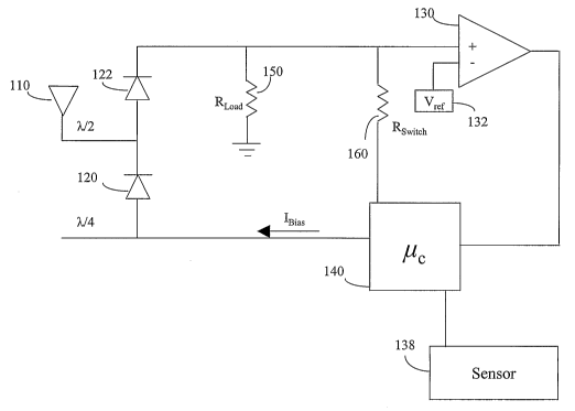
FIG 4 is a schematic of a RFID tag according to one embodiment of the present
invention showing an additional resistor, Rs~,;t~n engaged to provide a low
impedance load
to increase the bias current during bacl~scatter mode.
DETAILED DESCRIPTION
In a first aspect of the present invention, a radio frequency (RF)
communication
device is provided comprising means for switching between a low current
operating mode
and a high current operating mode. The low current operating mode is optimized
to
conserve power while the RF device is awaiting a wale-up signal from an
interrogator.
The high current operating mode is optimized to provide antenna matching
during
bacl~scatter communications so as to maximize the range of bacl~scatter
communication
between the RF device and the interrogator.
In a preferred embodiment of the present invention, the remote RF
communication
device comprises a radio frequency identification tag. The description of the
preferred
embodiments of the present invention will be discussed with reference to a RF
tag and RF
transponder as the RF communication device.
In one aspect of the present invention, the RF communication system comprises
an
interrogator and at least one RF communication device comprising an RF tag.
Referring
now to FIG. 2, a diagram of one embodiment of a conununication system of the
present
invention is illustrated. The communication system 210 comprises an
interrogator 212
and a plurality of remote communication devices 214, 216, and 218.
Each remote communication device 214, 216, and 218 within the system 210
comprises: a remote communication device antenna 226 operable to receive and
backscatter a carrier signal 222. The bacl~scattered carrier signal 224
comprises the
carrier signal and a secondary signal with data encoded therein. The remote
communication devices 214, 216, and 218 further comprise a signal processing
circuit
coupled to the remote communication device antenna 226. The signal processing
circuit
comprises at least one encoding circuit operable to encode binary data into
the
bacl~scattered carrier signal.
6
CA 02532875 2006-O1-13
WO 2005/020444 PCT/US2004/024150
The interrogator 212 comprises an antenna 220 operable to receive a plurality
of
backscattered carrier signals 224 backscattered from the plurality of remote
communication devices 214, 216, and 218. The interrogator 212 further
comprises a
receiving circuit coupled to the antenna 220 operable to extract data from
each of the
backscattered carrier signals 224. Although three remote communication devices
214,
216, and 218 are illustrated, the system 210 may comprise any number of remote
communication devices.
In a further embodiment of the present invention, the interrogator 212 may
further
comprise a transmitting circuit coupled to the antenna 220, wherein the
transmitting
circuit is operable to transmit a carrier signal 222 to the plurality of
remote
communication devices 214, 216, and 218. In another embodiment, the anternza
220 may
comprise a transmitting antenna coupled to a transmitting circuit and a
receiving antenna
coupled to the receiving circuit.
In another embodiment, the remote communication device antenna 226 and the
signal processing circuit of the remote connnunication devices may be
configured to
generate a supply voltage from the carrier signal.
In another embodiment of the communication system 210, the remote
communication devices 214, 216, and 218 may further comprise a sensor coupled
to the
signal processing circuit, wherein the signal processing circuit is further
operable to
receive a sensor signal from the sensor, encode the sensor signal, and include
the encoded
sensor signal in the secondary signal of the backscattered carrier signal 224.
As used herein, a sensor includes any device that senses either the absolute
value
of or a change in a physical quantity such as, but not limited to,
temperature, pressure,
intensity of light, and acceleration. For example, any pressure sensor known
in the art
may be used in the practice of the present invention as long as it may be
functionally
connected to a remote communication device. In an embodiment, a pressure
sensor may
comprise a piezoelectric pressure sensor in which a voltage is applied across
a diaphragm
coated with piezo crystals. Those skilled in the art will recognize other
sensing means
that may be employed in the various embodiments of the present invention
without
altering the spirit or scope of the present invention.
The devices, systems and methods of embodiments of the present invention may
employ many standard RFID hardware technologies known to those of ordinary
skill in
7
CA 02532875 2006-O1-13
WO 2005/020444 PCT/US2004/024150
the art to which the features of the embodiments of the present invention have
been
added. Hardware methodologies can vary greatly within the scope of the present
invention, but the principle of switching between two distinct power
consumption modes
can be applied to numerous hardware configurations.
For example, commercially available microcontrollers such as, but not limited
to,
an MSP 430 series of microcontrollers from Texas Instruments include an on
board ring
or RC oscillator that can be adjusted in fine steps. The lnicrocontroller can
act as the
switch for the additional resistor (RsW;t~h) of the present invention. By
using pre-existing
hardware, the systems and methods of the present invention may be employed
without
much, if any, additional cost to the system.
Referring to FIG. 4, showing a simplified schematic illustrating the concepts
of an
embodiment of the present invention, the RF communication device comprises an
antenna
110, a power source, and signal processing circuitry. The signal processing
circuitry
comprises a comparator 130 and a microcontroller 140. The comparator 130
compares
signals received by the antenna 110 to a reference signal 132 and feeds the
results to the
lnicrocontroller 140. The microcontroller 140 controls the computing and short-
term
memory functions on the tag. Further, the microcontroller 140 accepts signals
from the
sensor 138 and encodes the signals for communication bacl~ to the interrogator
through
antenna 110 bacl~scatter methodologies.
In a preferred embodiment of the present 111Ve11t1Q11, the means for switching
between a low current operating mode and a high current operating mode
comprises the
addition of a low load resistor 160 (RsW;t~~,) and a switch for engaging and
disengaging the
low load resistor to the input of the microcontroller. When the signal
processing circuit
on the RF communication device detects an inconung signal fr om the antenna,
the switch
turns the low load resistor 160 "on" thereby shunting the primary resistor 150
(Rloaa) and
providing more current to the system.
In a preferred embodiment of the present invention, the low current operating
mode provides a low current voltage to the system. This low current voltage is
achieved
through a high impedance provided by the high load resistor 150 (R;oaa). This
provides
the necessary voltage to the comparator to effect the detection and comparison
of an
incoming RF signal from the antenna 110. An RF communication device may be
"idle"
in low current operating mode for significant lengths of time before an
interrogator signal
8
CA 02532875 2006-O1-13
WO 2005/020444 PCT/US2004/024150
is received. By operating in the low current mode during this time, the RF
communications device can effectively await instructions from the interrogator
while
using a minimal amount of power. When a signal is detected by the signal
processing
circuit, the circuit switches to high current mode.
In a preferred embodiment of the present invention the low load resistor 160
is
selected such that the high current operating mode produces a high bias
current (Iv;as) to
the system, and particularly to the antenna. The desired effect is a high
matching of the
antenna such that the impedance of the circuit closely approximates that of
the antenna.
By providing a low source impedance and therefore a high load to the antenna,
such that
the source impedance matches the antenna impedance, the bacl~scatter range of
the RF
communication device may be maximized for the given system.
In one embodiment of the present invention, provided to illustrate an
exemplary
configuration, the RF tag comprises a power source of 2.8 volts. In this
configuration,
prior art systems would have a standard load resistor of approximately 1 Mega
ohms to
allow for relatively good bacl~scatter range up to 10 Mega ohms to reduce
power
consumption during listening mode. In either case, the bacl~scatter range
could not be
optimized due to the draw on the battery during listening mode. The present
invention
replaces this configuration with a high load resistor 150 (R;oaa) of between
about 1 and
about 10 Mega ohms, and the switchable low load resistor 160 (RsW;t~~,) of
about 1000
ohms. In the present configuration, power consumption can be nuninuzed through
the
high load resistor, and the low load resistor can provide antema matching
during
bacl~scatter.
In this example, the difference in resistance between Rloaa and RsW;t~n is
approximately 103 to 104. This allows the RF tag a broad range between the low
current
and high current operating modes to provide significant power savings during
listening
mode, and nearly perfect antenna matching achieved during baclcscatter mode.
Through
this configuration and technique, the bacl~scatter range can typically be
doubled as
compared to a traditional RF tag optimized for power consumption. In an
exemplary
embodiment of this feature, a prior art system optimized for power consumption
employed a 1 Mega ohm load resistor. This system was able to baclcscatter
about 5 feet
when introduced to a 1 megawatt interrogator. To contrast, a system of the
present
invention employed a 1 Mega ohm load resistor and a 2.5 lcilo-ohm switchable
resistor,
9
CA 02532875 2006-O1-13
WO 2005/020444 PCT/US2004/024150
and was able to backscatter 15 feet with no loss in reception. This reflects a
three-fold
increase in backscatter range as compared to a similar prior art system.
The precise values for Rloaa and RsW;t~h will be appreciated by those skilled
in the
art for a given RF transponder, and will be designed based on the needs of the
system.
However, the principles taught herein are applicable to RF transponders that
would
benefit by having two operating modes comprising different optimized power
requirements. As previously discussed, the ideal system would provide a high
resistive
value for Rloaa so as to mininuze power usage during listening mode, and an
appropriate
resistive value for Rs~;t~h so as to provide antenna matching and maximize
backscatter
range.
Although the present invention has been described with reference to particular
embodiments, it should be recognized that these embodiments are merely
illustrative of
the principles of the present invention. Those of ordinary shill in the art
will appreciate
that the apparatus and methods of the present invention may be constructed and
implemented in other ways and embodiments. Accordingly, the description herein
should
not be read as limiting the present invention, as other embodiments also fall
within the
scope of the present invention.