Note: Descriptions are shown in the official language in which they were submitted.
CA 02533086 2006-12-14
WO 2005/015721 PCT/II820041019301
PtOGRA1VIlVIABLE POWER CO + RTER
S TECHWCAY. FIELD OF THE INYENTION
7,'he present invontion generally relates to the field of power converters,
and, more partiauiarly, to programmable power converters.
BACICCROYfiiD OF THE IlvVENTION
As the use of rnobile electtonic products continues to increase, such as PC
notebooks, PDAs , cellular telephones, MP3 players azd the like, the need for
low cost, compact power supplres and solutions to power and reahargc thcse
-1-
CA 02533086 2006-01-18
WO 2005/015721 PCT/US2004/019301
products also continues to increase. Most manufacturers of mobile products
typically provide plug-in power adapters along with these mobile products to
help
provide the power supply needs of their customers.
Today's power adapters are typically AC-to-DC, or DC-to-DC power
converters which are configured to convert an AC voltage to a DC voltage, or
step-up or step-down the DC voltage input delivered to the mobile device. With
AC-to-DC adapters, for example, users can power most mobile devices by simply
plugging the adapter into a standard AC wall outlet commonly found in most
homes and offices. Similarly, when only DC input power is available, such as
in
an automobile or airplane, users can still power their mobile devices by
siinply
using a standard, off-the-shelf DC-to-DC adapter, such as with a cigarette
ligllter
connector. Normally, both adapters are designed and tailored to provide a
regulated DC output voltage, which voltage typically ranges from between 5VDC
to 30VDC depending on the power requirements of mobile device being powered.
Altliough these power adapters conveniently provide direct power and
recharging capabilities, users are often required to carry separate adapters
to
provide power to each individual mobile device. This often means that users
have
to carry multiple adapters for each device: one for an AC input power source,
and
another for a DC input power source. Moreover, users with multiple devices are
typically required to carry multiple adapters to power all the multiple
devices,
thereby increasing the amount of bullc a user is required to carry, which is
also
tedious.
Accordingly, there exists a need for a power converter and system that
resolves the system power management problems associated with carrying all of
the different power supply components necessary to power a wide variety of
mobile and portable devices having different power requirements. Moreover,
-2-
CA 02533086 2006-01-18
WO 2005/015721 PCT/US2004/019301
there is a need for a power converter and system that is prograrrnnable for
providing power with selected electrical characteristics.
-3-
CA 02533086 2006-01-18
WO 2005/015721 PCT/US2004/019301
SUMMARY OF THE INVENTION
The present invention achieves technical advantages as a programmable
converter supplying programmable DC voltages adapted to power a plurality of
portable devices. In one embodiment of the invention, the converter receives a
DC
input signal or AC input signal, and provides a predetermined DC output
signal, and
includes circuitry responsive to the DC signal or AC input signal for
providing a
converted DC signal in which the converted DC signal has electrical
characteristics
wllich are selectable, and includes a controller cooperable with the circuitry
for
establishing the electrical characteristics based on a selection code.
In anotller embodiment, the converter includes a coupler coupled to the
circuitry in which the programming circuitry includes a socket adapted to
receive a
insertable memory device and electrically couple the programming circuitry and
the
memory device. The memory device for storing a code indicative of an
electrical
characteristic selection, wherein the code is readable from the memory by the
programming circuitry for imposing the electrical characteristic selection
upon the
converted DC signal.
-4-
CA 02533086 2006-01-18
WO 2005/015721 PCT/US2004/019301
BRIEF DESCRIPTION OF THE DRAWINGS
Advantages of the invention and the specific embodiments will be
understood by those of ordinary skill in the art by reference to the following
detailed description of preferred embodiments taken in conjunction with the
drawings, in which:
Figure 1A shows a block diagram of a dual input AC and DC power
converter having dual DC voltage outputs in accordance with the present
invention;
Figure 1B shows an exploded view of the converter with the detacllable
buck circuit;
Figure 2 sliows a schematic diagram of the power converter circuit as
illustrated in Figure 1 in accordance with the present invention;
Figure 3 shows a detailed schematic diagram of a DC-to-DC buck
converter circuit in accordance with the present invention;
Figure 4 is a perspective view of a power converter system including a
power converter adapted to receive both an AC and DC voltage input, and a
peripheral power hub (PPH) according to the present invention;
Figure 5 is an electrical block diagram of one preferred embodiment of the
PPH shown in Figure 4, where each of the outputs of the PPH are connectable to
an associated selectively attachable buck circuit providing a selectable
voltage to
an associated remote device;
-5-
CA 02533086 2006-01-18
WO 2005/015721 PCT/US2004/019301
Figure 6 is an electrical block diagram of another preferred embodiment
whereby the PPH includes a plurality of programmable buck circuits, each
having
a selectively removable programming device, shown as a resister Rl, whereby
each remote mobile device can be directly coupled to a PPH output as sllown;
and
Figure 7 illustrates a block diagram of a dual input AC and DC power
converter having DC voltage outputs in accordance with exemplary embodiments
of the present invention.
-6-
CA 02533086 2006-01-18
WO 2005/015721 PCT/US2004/019301
DETAILED DESCRIPTION OF THE PREFERRED EMBODIMENT
The numerous innovative teachings of the present applications will be
described with particular reference to the presently preferred exemplary
embodiments. However, it should be understood that this class of embodiments
provides only a few examples of the many advantageous uses and innovative
teachings herein. In general, statements made in the specification of the
present
application do not necessarily delimit any of the various claimed inventions.
Moreover, some statements may apply to some inventive features, but not to
others.
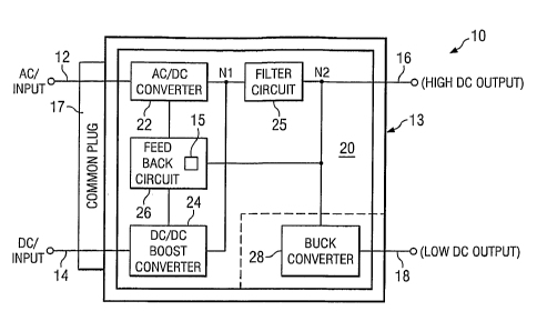
There is shown in Figure 1A a block diagram of a dual input AC/DC
power converter 10 having dual programmable DC voltage outputs in accordance
with the present invention. Preferably, the dual input AC/DC power converter
10
comprises a power converter circuit 20 having an AC-to-DC converter 22, a DC-
to-DC booster converter 24, a feedback circuit 26, a filter circuit 25 and a
DC-to-
DC buck converter 28. The power converter circuit 20 is seen housed in housing
13 and advantageously provides a first programmable DC output voltage at DC
output terminal 16 and a second programinable DC output voltage at terminal
18.
Both of these DC output voltages may be generated as a function of both AC and
DC input voltages.
In operation, the AC-to-DC converter 22 receives an AC signal via input
terminal 12 and provides a regulated DC output voltage at node N1. Similarly,
the
DC-to-DC booster converter 24 may receive a DC input voltage at its input via
input terminal 14 and may also provide a regulated DC output voltage at node
N1.
Input terminals 12 and 14 are integrated into a single common connector
17 such that different power cords adapted to receive input power from
different
sources are received by the common connector 17. For instance, DC power from
-7-
CA 02533086 2006-01-18
WO 2005/015721 PCT/US2004/019301
an airplane or car power source are wired to couple to input 14 and AC source
is
wired to couple to input 12. In a selected embodiment, the AC-to-DC converter
22 is adapted to generate a DC output voltage of between 15VDC and 24VDC in
response to an AC input voltage at terminal 12 ranging between 90VAC and
265VAC. Likewise, the DC-to-DC booster converter 24 is adapted to provide a
DC output voltage which is substantially similar to that of converter 22, but
which
is generated in response to a DC input voltage supplied at input terminal 14.
Preferably, DC-to-DC booster converter 24 is adapted to receive a voltage in
the
range of between 1 1VDC and 16VDC. Advantageously, AC-to-DC conversion,
via AC-to-DC converter 22, allows users of the power converter 10 to power
high-power mobile devices, such as a laptop computer wherever AC input power
is available, such as in the home or office, for exainple. Conversely, the DC-
to-
DC booster converter 24 of the power converter 10 is capable of powering
similar
high-power devices by stepping up most low amplitude DC input signals, such as
those found in automobile and/or airplane environments.
As shown, filter circuit 25 has its input tied to the respective outputs of
the
converter 22 and 24. In a preferred embodiment, the filter circuit is adapted
to
provide a filtered DC output voltage at second node N2, which, thereafter,
feeds
output terminal 16, at an output power of 75 watts, for example.
The single feedback circuit 26 is shown coupled to the output of filter
circuit 25 at node N2. In a preferred embodiment, the feedback 26 circuit,
through a single feedback loop, regulates the voltage level of the filtered DC
output voltages generated by both converters 22 and 24. Additionally, the
feedback circuit 26 is adapted to receive a removable programming module that
allows mobile device users to provide a selectable DC output voltage at output
16
via node N2. The programming module comprises a key 15 comprising a resistor,
wherein different associated values of the resistor establish different
associated
-8-
CA 02533086 2006-01-18
WO 2005/015721 PCT/US2004/019301
DC output voltages at output 16. By allowing users to selectively change the
voltage level of the filtered DC output voltage, the power converter 10 may be
adapted to power a variety of different mobile electronic devices, having
different
associated power requirements. Moreover, the power converter's 10 programining
module may also be adapted to provide the additional function of output
current
limiting.
The DC-to-DC buck converter 28 has its input coupled at node N2,
providing a second DC output voltage that is then fed to output terminal 18,
having an output power of 10 watts, for example. Preferably, buck converter 28
discreetly steps down the filtered DC voltage and produces a second DC output
voltage at a separate output terminal 18. In a selected embodiment, the buck
converter 28 steps down the filtered DC output voltage to a range of about
3VDC
and 15VDC. Advantageously, this second DC output voltage generated by
converter 28 is independent of, and substantially lower than the DC output
voltage at terminal 16. This allows users of the present invention to power
not
only a high-power peripheral, such as a laptop computer, but also, a second,
low-
power peripheral, such as a cell phone, PDA, and the like. Moreover, the
present
invention allows for these peripherals to be powered simultaneously by a
single
converter, regardless if the input voltage is AC or DC. The buck converter 28
is
physically detachable from the main housing 13 as shown in Figure 1B, allowing
different buck circuits providing different output voltages to be selectively
attached to housing 13 and tap the DC output voltage from output tenninal 18.
Refeiring now to Figure 2 there is shown a schematic diagram of the
power converter circuit 20 of the dual input AC/DC power converter 10 as
depicted in Figure 1 in accordance with an exemplary embodiment of the present
invention. As described herein in greater detail, the power converter circuit
20, in
-9-
CA 02533086 2006-01-18
WO 2005/015721 PCT/US2004/019301
a preferred embodiment, comprises three separate converters: AC-to-DC power
converter 22, DC/DC boost converter 24, and DC-to-DC buck converter 28.
AC-TO-DC CONVERTER
The AC-to-DC power converter 22 includes a true off line switcher which
is configured in a fly-back topology. Full-wave rectification of an AC input
signal, received at input terminal 12, occurs using a full-wave bridge
rectifier
BD1 and a filter capacitor Cl, which creates a DC voltage bus from which the
switcher operates. Inductor Ll offers additional EMI filtering of the AC
signal
after the signal has been rectified through the full-wave bridge. The AC-to-DC
converter 22 also includes a main controller ICl configured as a current mode
pulse-width modulator (PWM). Main controller ICl is also configured to have a
single-ended output with totem pole driver transistors coupled thereto. The AC-
to-DC power converter 22 has a main power switch Q7 which drives the main
transformer T1. In a preferred embodiment, the transformer Tl, Schottky diode
D11, and filter capacitors C24 and C25 combine to provide the DC output
voltage
at node Nl.
As noted earlier, filter circuit 25 allows for additional filtering of the DC
output voltage derived from node Nl. The filter circuit 25 itself comprises
inductor L3, capacitor C26 and transformer NF1. Advantageously, the filter
circuit 25 produces a filtered DC output voltage at output 16 having less than
100mv peak-to-peak noise and ripple.
The feedback circuit 26, tlirough a single feedback loop, is capable of
regulating the filtered DC output voltages provided by the converters 22 and
24.
The feedback circuit 26 is also adapted to be coupled to a reinovable
programming module having a key 15, comprising resistor R53. As such, the
-10-
CA 02533086 2006-01-18
WO 2005/015721 PCT/US2004/019301
present invention allows users to selectively program the DC output voltage
later
received at output terminal 16. The feedback circuit 26 includes a
photocoupler
circuit comprising a pair of photocouplers PH1 and PH3 connected in series
(i.e.,
stacked), each being coupled to the outputs of operational amplifiers IC4-A
and
IC4-B. Advantageously, these photocouplers are arranged along the feedback
loop of the feedback circuit 26 with photocoupler PH1 and PH3 coupled
respectively to converters 22 and 24. Through a single feedback loop, the
feedback circuit 26 efficiently regulates the filtered DC output voltage
provided at
node N2. Moreover, by stacking the photo-couplers, the present invention also
allows the power converter 10 to maintain proper input/output isolation
between
respective terrninals 12 and 14 and output terminal 16.
Preferably, the output current limiting function of converter 22 is
accomplished via integrated circuit IC4A, resistors R33, R37, R38, and R39 and
programming resistor R54.
Over voltage protection of AC-to-DC converter 22 is achieved using
photocoupler PH2 and zener diode ZD2. In a preferred embodiment, zener diode
ZD2 is set at 25V such that when in avalanche mode it causes the transistor
side
of photocoupler PH2 to bias transistor Q1 into the on state. When it is the on
state, transistor Q3 pulls low pin 1 of integrated controller IC 1 and pulls
the
operating duty cycle of the integrated controller towards 0%. This takes the
DC
output voltage to 0 volts. Also, when transistor Q1 is on, transistor Q2 is
also
forced on which then forces these two transistors become latched. If
transistors
Q1 and Q2 are latched, input power must be recycled in order for the power
converter 10 to be turned on again.
-11-
CA 02533086 2006-01-18
WO 2005/015721 PCT/US2004/019301
DC-TO-DC CONVERTER
The DC-to-DC converter 24 is configured in a boost topology and utilizes
the same kind of integrated controller, IC2, as used in converter 22. In the
DC-to-
DC converter 24, transistor Q8 acts as the main power switch and diode D8 as
the
main rectifier. Preferably, inductor L2 is adapted to function as a power
boost
inductor, which is comprised of a toroid core-type inductor. It should be
understood that the cathode leads of diodes D11 and D8 are connected, forming
an ORed configuration, requiring only one output filter. Advantageously, this
eliininates the board space needed for a second set of filter capacitors.
Like the AC-to-DC converter 22, the DC-to-DC converter 24 is also
designed to operate at a frequency of around 80KHZ. For the AC-to-DC converter
22, the operating frequency is set by resistor R13 and capacitor C7. Likewise,
the
operating frequency of the DC-to-DC converter 24 are set by resistor R28 and
capacitor C16.
The DC-to-DC converter 24 includes an over-voltage protection circuit
comprising zener diode ZD2, resistor R23, R24, R48, transistor Q4, and silicon-
controlled rectifier SC1. Zener diode ZD2 sets the over-voltage protection
point
(OVP) which is preferably set at 25VDC. Generally, there is no current flowing
through resistor R48. If, however, when zener diode ZD2 begins to conduct
current, the drop across R48 is significant enough to bias transistor Q4 on,
pulling
its collector terminal high, and thereby turning silicon controlled rectifier
SC1 on.
When silicon control rectifier SC1 is on, it pulls pin 1 of the integrated
controller
IC2 low. Thus, if pin l of integrated controller IC2 is low, the output
drivers
thereof are forced to operate at a duty cycle of 0%, thereby producing a DC
output
-12-
CA 02533086 2006-01-18
WO 2005/015721 PCT/US2004/019301
voltage of 0 volts at IC2 pin 6. Advantageously, the silicon controlled
rectifier
SC1 functions as a power latch circuit that requires that input power be
recycled
in order to turn on the power converter 10 if a voltage above 25VDC is
detected at
node Nl.
The temperature of the housing 13 of the power converter 10 is monitored
using a thermistor NTC3. If, for example, there is a corresponding increase in
the
temperature of the housing 13, it will result in a decrease in the resistive
value of
tliermistor NTC3, thereby causing transistor Q9 to turn on and pull low pin 1
of
integrated circuit IC2 of converter 24. Moreover, this causes the photo-
coupler
PH2 to be biased enough to activate a latch circuit comprising transistors Q1
and
Q2 that will shutdown the power converter 22. In addition, the power
converter's
10 thermal protection feature is adapted to operate regardless of whether an
AC or
DC input voltage is being received at their respective input terminals.
Figure 3 shows a detailed schematic diagram of the DC-to-DC buck
converter 28 in accordance with the present invention. The buck converter 28
has
an integrated circuit controller ICl, similar to converters 22 and 24, which
is
adapted to generate an on-time duty cycle to power transistor switch Q1. The
operating frequency of controller IC1 is set by capacitor C6, which is coupled
between pin 4 of IC1 and ground, and resistor Rl, which is coupled between
pins
4 and S. In a selected embodiment, the diode Dl functions comprises a Schottky
diode and functions as "catch" diode. Inductor Ll is a output power inductor
and
couples the source of power transistor Q1 to Vot,t. Fuse Fl is shown coupled
between V;,, and the drain terminal of power transistor Q1, and advantageously
provides current protection to buck-converter 28.
Furthermore, the input V;,, of the buck converter 28 is coupled to the
output of filter circuit 25 at node N2, wherein V;,, receives the filtered DC
output
-13-
CA 02533086 2006-01-18
WO 2005/015721 PCT/US2004/019301
voltage therefrom. In a preferred embodiment, the buck converter 28 provides a
second DC output voltage at Vout, coupled to output terminal 18.
Advantageously,
the buck convert 28 discreetly steps down the filtered DC output voltage and
provides a second DC output voltage at output terminal 18 which is independent
of, and substantially lower than the DC output voltage at output terminal 16.
Likewise, the DC output voltage of the buck converter 28 enables users of the
present invention to power low-power peripherals, such as, cell phones, PDAs,
and/or similar mobile devices. In a selected embodiment, the buck converter 28
may also be adapted to provide a DC output voltage at output terminal 18
ranging
between 3VDC and 15VDC, selectively detennined as a function of the chosen
value of resistor R2 used in the particular buck converter 28, with a total
power
delivery of 10 watts, for example. As previously mentioned, the buck converter
28 may be housed in a separate, detachable program module that enables users
to
selectively program the DC output voltage at terminal 18 as a function of
different
associated buck converter modules.
Referring now to Figure 4, there is generally shown at 40 a perspective
view of a peripheral power system (PPS) seen to include the AC/DC-to-
programmable DC output converter 42 as shown and described in reference to
Figures 1-3. In addition, PPS 40 is also seen to include a peripheral power
hub
(PPH) shown at 44 and having a plurality of DC voltage outputs generally shown
at 46. As will be described in more detail shortly, in one preferred
embodiment
(Figure 5) predetermined DC voltages are provided at each output which may
then be converted by a buclc circuit 28 associated with the peripheral device
72 to
be powered. In another preferred embodiment (Figure 6) each of these outputs
46
is programmable as a function of a removable programming key, such as a
selectively replaceable programming resistor. Converter 42 provides a
predetermined output DC voltage, which may be programmable, via a DC voltage
-14-
CA 02533086 2006-01-18
WO 2005/015721 PCT/US2004/019301
coupler 48 to a primary device, such as a notebook computer 50, requiring a
higher operating voltage and consuming a large amount of power, such as 45
watts. DC voltage coupler 48 also provides tapping of this output DC voltage
provided to the primary device 50, which voltage is tapped via a connector 52.
In the embodiment shown at 60 in Figure 5, the input voltage provided to
input 62 is muxed to the plurality of output ports 46. The separate buck
circuits
28 associated with and selectively coupled to the associated remote mobile
device
72 convert this voltage to the final output voltages V1-V4 as shown in Figure
5,
which meets all the power needs of the associated mobile device 72. According
to the embodiinent shown at 70 in Figure 6, the plurality of buck circuits 28
are
integral to the PPH 44, each buck circuit 28 having a selectively removable
programming key, shown as resistor Rl, providing a programmable DC voltage to
the respective output port 46 commensurate with the requirements of the
associated remote mobile 72 device. Output ports 46 may be configured as
simple pin type connectors, USB type connectors, and other configurations as
desired. Again, the buck circuit 28 could be substituted with a boost circuit
if
desired to provide a higher voltage.
Turning now to Figure 5, there is shown the first embodiment of the
present invention comprising the PPH 44 shown in Figure 4. As previously
mentioned, the input DC voltage provided to the PPH 44 at input 62 is coupled
to
each of the output ports 46 by a voltage mux 64. This coupling of the input DC
voltage to the multiple output ports 46 can be accomplished in a number of
ways,
such as via a simple resistive divide network, and may provide output-to-
output
isolation. In one implementation, the DC voltage provided at input 62 is
directly
provided to the output ports 46 for a subsequent down-stepping via the
associated
buck circuit 28. However, a lower voltage can be provided by the voltage mux
64
to each of the output ports 46 if desired. Voltage mux 64 is also seen to
include
-15-
CA 02533086 2006-01-18
WO 2005/015721 PCT/US2004/019301
an over load protection circuit generally shown at 66 which limits the amount
of
power that can be provided to each output port 46, such as 7 watts, to prevent
overload of the PPH 44, and to prevent power hoarding at one output by its
associated reinote device 72 to the determent of the other reinote devices 72.
Visual indicators 68 are provided to visually indicate the status of each
output port 46. For instance, the LED 68 associated with each of the output 46
may be illumiinated as green when power provided via output port 46 is below a
predetermined limit, such as 7 watts each. If, however, a remote device 72
associated with the particular buck circuit 28 is attempting to draw more than
the
predetermined limit, the voltage mux 64 prevents providing power in excess of
this predetermined limit, and also illuminates the associated LED as red
indicating
an atteinpted over power condition. Thus, a user can visually ascertain
whether or
not power being provided to the associated output port 46 is within an
acceptable
range as visually indicated by an associated green LED 68, or, that the
associated
remote device 72 is attempting to draw more than the predetermined limit. The
voltage mux 64 also includes a main fuse 69 preventing excessive power draw of
the PPH 44 itself, which could otherwise cause an overload condition to the
power converter 42 or other input power source.
The advantages of the embodiment 60 shown in Figure 5 include that a
separate buck circuit 28 and the associated cord can be simply coupled to any
of
the output ports 46 and provide a programmable DC output voltage meeting ther
needs of the associated remote device 72. A user having a buck circuit 28/cord
for use with the particular remote device 72 can be plugged into any of the
available output ports 46 of the PPH 44. The DC voltage is stepped down by
buck circuit 28 external to the housing of PPH 44. This solution is low cost
and a
simple design.
-16-
CA 02533086 2006-01-18
WO 2005/015721 PCT/US2004/019301
Turning now to Figure 6, there is shown at 70 another preferred
embodiment of the present invention whereby a plurality of buck circuits 28
are
provided within the PPH 44 to provide a programmable output DC voltage to the
respective output port 46. Each buck circuit 28, as shown in Figure 3, has an
associated programming resister Rl which may be selectively removable from the
PPH 44 to selectively establish the output DC voltage provided to the
associated
output port 46. Thus, the DC output voltage at each output port 46 is
selectively
prograrmnable, and a remote device 72 need to only utilize a standard two
conductor cord to couple to output port 46, as shown. Namely, one conductor
couples the programinable output voltage V1, and the other conductor provides
the ground. Again, each buck circuit 28 could be substituted with a boost
circuit
if desired.
Advantages of this embodiment 70 include that the buck circuits 28 are
enclosed in the PPH 44, where each buck circuit 28 itself may be programmable
using the associated programming resistor Rl. In this arrangement, care must
be
talcen that the remote device 72 is coupled to an output port having a
desirable
output voltage. Thus, the keys provide indicia of the output voltage being
provided. The voltage mux 64 simply provides the input voltage at input 62 to
each of the buck circuits 28, which may step down (or step up) the voltage
thereat. Voltage mux 64 includes the overload protection circuit 66, the
associated LED's 68, and the hub main fuse 69 as shown.
Both embodiments 60 and 70 provide a DC peripheral power hub adapted
to power a plurality of unique remote devices 72 from a single unit 44, such
remote devices including a cell phone, PDA, MP3 player, etc. This peripheral
power hub 44 may be an accessory to power converter 42, or, a stand alone
device
receiving power. For instance, the input cord 52 feeding PPH 44 may be
directly
coupled to an output of converter 42, as shown in Figure 4, tapped from the DC
-17-
CA 02533086 2006-01-18
WO 2005/015721 PCT/US2004/019301
coupler 48 without any down stepping by a buck circuit 28, or directly coupled
to
a DC source, such as via a cigarette lighter outlet, or other input source.
According to yet another preferred embodiment, as shown in Figure 7, the
power converter 10 include programming circuitry 726, such as a micro-
controller
(computer chip). The programming circuitry 726 is cooperable with converters
22
and 24, and filter 25 for effectuating a program for setting the electrical
parameters
associated with the output signals 16 and/or 18, such as the output voltage,
output
current, output power, current limit, polarity, over voltage protection
threshold,
and/or other electrical parameters associated with each of the output signals
16 and
18. Programming signaling/feedback occurs through communication lines 722 and
724. For example, the converter 10 with a micro controller inside, adjusts the
numerical value of sensing resistor(s) or reference voltage(s) (shown in
Figures 2 and
3) to effectuate a determined output voltage(s), output current(s) or output
power.
The programming circuitry 726 can include memory 715 for data and program
storage, hardware, and/or software which enables start-up and control for
effectuating the above-mentioned electrical properties. In a preferred
embodiment,
the programming circuitry 726 is powered from the converted signal of either
converters 22 or 24.
Data indicative of electrical parameter selection is storable by the
programming circuitry 726 in memory 715, such that on a power-up condition the
data is read and the associated electrical parameters of the signal output 16
and/or 18
are effectuated by the programming circuitry 726. This data can be programmed
into
the programming circuitry 726 and subsequently into the memory 715 from
outside
the power supply unit. That way, by changing the data that is provided to the
programming circuitry 715 and memory, the characteristics of the supplied
signal can
be changed at will. For example, the data can be provided to the programming
circuitry 726 at the time of production or by an OEM vendor w11o might stock
-18-
CA 02533086 2006-01-18
WO 2005/015721 PCT/US2004/019301
standard power supply units and then program each one for a specific
customer's
needs. This process would be akin to activating a new cell phone with the
customer's
information. The data can also be provided by the peripheral device 72 to be
powered, such that the device 72 programs the programming circuitry 715 to
effectuate electrical paraineters required for the device 72.
The data can be provided from a source 710 external to the converter 10 (such
as a program controller) via a simple 2 pin connector, infra-red or visible
optical
signaling, magnetic induction, acoustic signaling, etcetera. Transmission
mediums
725 for communication between the external source 710 and the converter 10
include
both wired mediums (such as coaxial cable, twisted pair wire, fiber-optic
cable) and
wireless mediums. The converter 10 can also include an interface 720 for
interfacing
between the different signaling types and transmission mediums, and the
programming circuitry 715. Thus, as can be understood, the converter 10 can be
programmed via communication systems such as the Internet to deliver data,
analog
and/or digital, from an external source to the converter 10.
In yet another exemplary embodiment, the programming circuitry 726
includes an EPROM 715 which forms a portion of the circuitry. The EPROM
715 can be permanently affixed in the converter 10 or selectively insertable
into,
and removable from an EPROM socket (i.e., keyway). The EPROM is
programmed external of the converter 10 (using an EPROM burner, for example),
and then inserted into the socket to effect the desired output
characteristics.
Advantageously, the EPROM chip could be programmed at the time of purchase,
and then installed by a salesman into the converter. Advantageously, several
EPROM chips can each be programined for different output characteristics and
selected from and inserted as the intended use changes. An EEPROM may also
be utilized in place of the EPROM to prevent the need to install different
EPROMS for different output programming.
-19-
CA 02533086 2006-01-18
WO 2005/015721 PCT/US2004/019301
Though the invention has been described witl7 respect to specific preferred
embodiments, many variations and modifications will become apparent to those
skilled in the art upon reading the present application. It is therefore the
intention
that the appended claims be interpreted as broadly as possible in view of the
prior
art to include all such variations and modifications.
-20-