Note: Descriptions are shown in the official language in which they were submitted.
CA 02533331 2006-O1-19
WO 2005/015638 PCT/EP2004/008007
PROCESS FOR MANUFACTURING A SOLAR CELL FOIL USING A
TEMPORARY SUBSTRATE
The invention pertains to a process for manufacturing a solar cell unit using
a
temporary substrate. The invention also pertains to the solar cell foils thus
obtained.
Solar cell foils, also known as photovoltaic foils, generally comprise a
carrier
and a photovoltaic (PV) layer composed of a semiconductor material provided
between a front electrode comprising a transparent conductive oxide (TCO) (at
the front of the foil) and a back electrode (at the back of the foil). The
front
electrode is transparent, enabling incident light to reach the semiconductor
material, where the incident radiation is converted into electric energy. In
this
way light can be used to generate electric current, which offers an
interesting
alternative to, say, fossil fuels or nuclear power.
WO 98/13882 and W099/49483 describe a method for manufacturing a
photovoltaic foil comprising the steps of providing a temporary substrate,
applying the transparent conductive oxide, applying a photovoltaic layer,
applying the back electrode layer, applying the carrier, removing the
temporary
substrate, and, preferably, applying a transparent protective top coat on the
transparent conductor layer. This method enables the roll-to-roll manufacture
of
a photovoltaic foil or device, while at the same time making it possible to
use
any desired transparent conductor material and deposition process without
jeopardizing the current-generating action of the PV layer. In WO 98/13882 an
etch resistant may be used to cover the non-adjacent most left and most right
transparent conductor tracks to provide electric contact between these side-
tracks and the side electrodes, By allowing in such manner part of the
temporary substrate to remain in place these contacts do not need to be
applied
separately. WO 01/78156 and WO 01/47020 describe variations on this
process.
CA 02533331 2006-O1-19
WO 2005/015638 PCT/EP2004/008007
2
The maximum voltage of a solar cell is determined by the intensity of the
incident light and by the composition of the cell, more particularly, by the
nature
of the semiconductor material. When the surface area of the solar cell is
increased, more power is generated, but the voltage remains the same. In order
to increase the voltage, a solar cell foil is often divided into different
cells, which
are connected in series. This is done by providing grooves in the solar cell
electrode layers, e.g., by using a laser or by means of etching or any other
patterning method, and establishing a conductive contact between the front
electrode of one cell and the back electrode of another, while interrupting
the
front electrode and the back electrode each at a different side of the
interconnect so as to prevent short-circuiting. When a solar cell foil is
employed,
the individual cells are held together by the carrier. The above-mentioned
patent
applications describe various ways of effecting the series connection.
It has appeared, however, that the photovoltaic foils prepared by the
processes ,~.
described in the above references may suffer from loss of quality when they
are°°~~~
provided with a series connection. It was found to be difficult to provide
photovoltaic foil with a homogeneous and high product quality. More in
particular, it was found that during the removal of the temporary substrate by
etching, the TCO layer may be damaged at the location of the interconnect.
During the etching step, the etchant may permeate the damaged TCO layer and
enter into the interconnect, therewith disrupting it. One of the problems is
the
possibility of occurrence of short-circuit between two separated parts of TCO
layer by remaining temporary substrate. There is therefore a need for a more
robust process for preparing a solar cell foil provided with a series
connection
via a temporary substrate, one which results in a more homogeneous product of
higher quality and minimal short-circuit problems. The present invention
provides such a process.
The present invention thus pertains to a process for manufacturing a solar
cell
foil comprising the steps of:
~ providing an etchable temporary substrate
CA 02533331 2006-O1-19
WO 2005/015638 PCT/EP2004/008007
3
~ applying a front electrode of a transparent conductive oxide (TCO) onto the
temporary substrate
~ applying a photovoltaic layer onto the TCO layer
applying a back electrode layer
~ applying a permanent carrier
~ ensuring that the front electrode and the back electrode are electrically
connected in an interconnect to establish a series connection, the front and
the back electrode each being interrupted by front and back groove,
respectively, at different sides of the interconnect
~ in any one of the preceding steps providing an etch resist on the non-TCO
side of the temporary substrate at least at the location of the interconnect,
and at least not at the entire location of the front groove
~ selectively removing the temporary substrate where it is not covered with
etch resist.
The result of the process according to the invention is that at the location
of the
interconnect parts of the temporary substrate remain on the TCO layer. The
presence of the resulting protective caps of temporary substrate material has
been found to improve the properties of the solar cell foil as regards
homogeneity and quality. More in particular, solar cell foils prepared by the
process according to the invention show fewer non-functioning cells than
comparable solar cell foils where the temporary substrate is removed in its
entirety.
The present invention also pertains to a solar cell unit comprising a front
electrode, a PV layer, and a back electrode layer, wherein the solar cell unit
is
divided into at least two individual cells connected in series, the series
connection comprising an interconnect which electrically connects the front
electrode of one cell with the back electrode of an adjacent cell, while the
front
and the back electrode are each interrupted at different sides of the
interconnect, in which solar cell unit a protective cap is present on the
front
CA 02533331 2006-O1-19
WO 2005/015638 PCT/EP2004/008007
4
electrode at the location of the interconnect, with the protective cap being
of a
different material than the interconnect. This solar cell unit can be obtained
through the process of the, present idea, but also through different
processes.
Preferably, the solar cell unit is a flexible solar cell foil suitable for
handling in a
roll-to roll process.
The process and the solar cell unit of the present invention have several
additional advantages.
In the first place, if the protective cap is made up of a conductive material,
e.g.,
when it originates from a temporary substrate made of a conductive material,
the protective cap can function as part of the interconnect, thus improving
the
conductive properties of the interconnect. This also allows for less stringent
control of the conditions applied in manufacturing the interconnect as regards
the properties of the TCO, because even if the TCO is damaged during the
manufacture of the interconnect, the presence of the protective cap of .
conductive temporary substrate material ensures that the interconnect will ~ w
function properly.
Further, by appropriate connection, the strip of temporary substrate remaining
on the TCO layer can be made to function as part of a current collection grid,
that is, a pattern of lines of a conductive material which is applied in such
a way
as to enable easy collection of the current carriers (electrons) generated in
the
photovoltaic layer and flowing through the electrode. As the solar cell does
not
generate energy at the location of the interconnect, the interconnect is an
ideal
location for the grid, since its presence at that location does not
detrimentally
affect the current-generating properties of the solar cell foil.
Further, the presence of conductive strips on the interconnect makes it easier
to
divide the solar cell foil into individual units, since the conductive strips
can be
formatted in such a manner that they can be used for attaching electrodes to
connect the solar cell foil to the "outside world".
In the context of the present specification, the term etching is intended to
mean
removing by chemical means, e.g., dissolution. An etchable substrate is a
CA 02533331 2006-O1-19
WO 2005/015638 PCT/EP2004/008007
substrate which can be removed by chemical means; an etch resist is a material
which can resist at least temporarily the conditions applied during the
removal
of the temporary substrate. The etch resist can be any material which can be
applied to the temporary substrate at the location of the interconnect and
which
5 will protect the temporary substrate at least temporarily from the action of
the
etchant. Various types of etch resist may be envisaged. In the first place,
there
is the etch resist which is resistant to the actions of the etchant and which
will
not be removed from the temporary substrate at some stage of the process.
This type of etch resist is indicated as a permanent etch resist. In contrast,
one
may also envisage a temporary etch resist, viz. an etch resist that will be
removed at some further stage of the process.
The formation of protective caps from the temporary substrate using the etch
resist may be effected in various ways. For example, one may apply an etch
resist, carry out the etching step, and optionally remove the etch resist in
some
further step. It may be that the temporary substrate is thicker than is
desired for w 4~
the protective cap. In that case, one can first etch part of the temporary
substrafie, then apply the etch resist, and subsequently remove the
unprotected
portion of the temporary substrate. In that case one may also first apply a
temporary etch resist, followed by partial removal of the temporary substrate
where it is not protected by an etch resist. Then, the temporary etch resist
is
removed and a further etching step is performed to reduce the thickness of the
protective cap. To effect the latter option it is also possible to use a
material
which is only temporarily resistant to the etchant. If this material, which is
in
effect an etch retardant, is used, the following will take place. At first,
the etch
retardant ensures that etching will take place only at the location where the
temporary substrate is not protected by the etch retardant. Then, when the
etch
retardant has dissolved, the etchant ensures that the fihickness of the
protective
cap is reduced.
A specific embodiment of the process of the invention is one in-which the etch
resist is a permanent etch resist the color of.which has been selected such
that
CA 02533331 2006-O1-19
WO 2005/015638 PCT/EP2004/008007
6
the caps on the interconnect have a color which matches that of the energy-
generating part of the solar cell unit or contrasts with it.
The color difference between the energy-generating part of the solar cell unit
and a colored interconnect cap can be expressed by way of the dEab, which is
defined as follows:
dEab = (dL2 + da2 + db2)'o2
wherein dL, da, and db are the difFerences in brightness, blueness, and
redness, respectively, between the parts provided with coloring material and
the
energy-generating parts of the solar cell unit. The L, a, and b values can be
determined in accordance with the CIELAB procedure using a D65 light source.
If the color of the interconnect caps is to match that of the solar cell unit,
the
dEab generally is below about 5, preferably below about 2, more preferably,
below about 0.3. In that case one can speak of the use of a camouflage color.
If
the color of the interconnect cap is selected to contrast with that of the
energy-
generating part of the solar cell unit, the dEab value generally is above
about
10, preferably above about 12, more preferably between about 20 and 100. If
more than one color is used, generally at least one of these colors will
satisfy
the above requirements for the dEab value.
The use of a combination of a distinguishing color and a matching color makes
it possible to decorate the solar cell unit with colored designs on a
homogeneous background. Examples of envisaged designs are patterns,
letters, figures, stripes, rectangles, and squares. In this embodiment,
generally
10-90% of the etch resist is provided with a distinguishing color, while 90-
10%
of the etch resist is provided with a camouflage color.
The application of the etch resist onto the temporary substrate can be carried
out at any stage in the process according to the invention. It can, e.g., be
applied before the beginning of the process, that is, before the application
of the
TCO onto the other side of the temporary substrate. (t can be applied at any
CA 02533331 2006-O1-19
WO 2005/015638 PCT/EP2004/008007
7
intermediate stage, and it can be applied at the end of the process, that is,
after
the application of the back electrode or, where applicable, the permanent
carrier, and just before removal of the temporary substrate by etching. The
latter
option is preferred, because it prevents the etch resist pattern from being
damaged during the preceding parts of the process. It also prevents the
presence of the etch resist pattern on the "back" of the temporary substrate
from interfering with the other processing steps. In the preferred roll-to-
roil
embodiment of the process according to the invention both may happen if the
temporary substrafie provided with a pattern in an etch resist on the back is
led
over one or more rolls. The application of the etch resist before the
application
of the transparent conductive oxide layer has the additional disadvantage that
the etch resist should be able to withstand the high temperatures which are
often applied in the deposition of the transparent conductive oxide layer.
95 In a preferred embodiment of the process according to the invention, the
temporary substrate is flexible, a flexible permanent carrier is applied, and
the
process is carried out by way of a roll-to-roll process.
The series connection
The manner in which the series connection is carried out is not critical to
the
present invention. In general, the series connection is established by
ensuring
that the front electrode of one cell and the back electrode of an adjacent
cell are
electrically connected in an interconnect while the front and the back
electrode
are each interrupted at different sides of the interconnect.
As indicated above, in each solar cell unit, the back electrode and the front
electrode (TCO layer) are interrupted, each at the other side of the
interconnect.
For both interruptions, the interrupting groove is present through the
electrode
layer itself and optionally also through the PV layer. For some of the
embodiments to be discussed below, the presence of the groove through the
PV layer will be described explicitly, but it' may be applied in general. It
should
CA 02533331 2006-O1-19
WO 2005/015638 PCT/EP2004/008007
8
be noted, however, that if the interrupting grooves are present through the
electrode layer and through the PV layer, care should be take to ensure that
the
electrode is not inadvertently short-circuited with the other electrode
through the
groove in the PV layer. Strips of an insulating material may be applied at the
location where the above-mentioned interrupting grooves are to be applied,
e.g., by laser-scribing. The insulating material will act as laser stop to
prevent
the formation of short-circuits by melting of the underlying material. For
some of
the embodiments to be discussed below, the provision of strips of an
insulating
material will be described explicitly, but they may be applied also in other
embodiments. The insulating material may be applied on the TCO layer and/or
on the PV layer, as applicable.
The interconnect can be established in various manners. It can be established
by applying a groove through the PV layer and filling it with a conductive
material. The groove may or may not extend through the TCO layer, through the
back electrode layer, or through - both the TCO layer and the back electrode ~
~N,
layer. This will depend, int. al., on the process step in which the groove is
applied. In one embodiment, the conductive material which is used to fill the
groove in the PV layer is back electrode material. If the PV layer is an
amorphous Si layer, the conductive connection can also be established by
fusing the amorphous Si layer with the back electrode. If the PV layer is an
amorphous Si layer, the interconnect can also be established by
recrystallising
the Si into a conductive material. This option is less preferred, however.
The sequence in which the interconnect and the interrupting grooves are
applied is not critical and will depend on what is most suitable in the
specific
process applied.
The width of the interconnect and the grooves interrupting the TCO layer and
the back electrode layer generally is determined by the following
considerations.
At the sites of the interconnect and the interrupting grooves, the solar cell
is
unable to convert light into electricity. In view of this, the interconnect-
and the
grooves have to be as narrow as possible. On the other hand, they have to be
CA 02533331 2006-O1-19
WO 2005/015638 PCT/EP2004/008007
9
wide enough to ensure that the desired effect, the interruption of the
different
layers and the connection of the front and the back electrode with sufficient
conductivity, is attained. The grooves interrupting the TCO layer and the back
electrode layer generally have a width of 2 to 200 ~,m, preferably of 5 to 75
~,m.
The interconnect generally has a width of 20 to 200 ~,m, preferably of 50 to
150
ym.
The strips of an insulating material that may be applied at the location where
the
above-mentioned interrupting grooves are to be applied should be wide enough
to allow for easy provision of the interrupting grooves within the width of
the
strips. In general, the strips have a width between 25 and 1,000 Vim,
preferably
between 50 and 400 ~,m, more preferably between 50 and 200 p.m.
The protective cap should be broad enough to ensure that the interconnect is
indeed protected. It generally extends at least 10 ~.m beyond the interconnect
at
both sides, preferably afi least 50 Vim. Generally, it will extend at most 200
~m
beyond the interconnect at both sides, preferably at most 100 ~,m. Obviously,
if
the protective cap is conductive, it may not extend beyond the groove
interrupting the TCO layer if that would mean that the two sides of the groove
would become electrically connected.
The grooves interrupting the front and back electrodes generally are
continuous
grooves, since the objective is to achieve proper insulation of the various
cell
strips. The interconnect, on the other hand, does not need to be continuous.
If
so desired, it may have a discontinuous form, taking the form of holes,
stripes,
or pits. For reasons of operational efficiency a continuous embodiment may be
preferred.
The invention is illustrated by the following figures.
Fig. 1 shows process steps for making an interconnect between two adjacent
cells of a solar module of the invention.
Fig. 2 shows another embodiment the solar module.
Fig. 3 shows process steps for making an embodiment of the solar module.
CA 02533331 2006-O1-19
WO 2005/015638 PCT/EP2004/008007
Fig. 4 shows process steps for making an embodiment having another
interconnect in the solar module.
Fig. 5 shows an embodiment the solar module with insulating strips.
Fig. 6 shows another embodiment the solar module with insulating strips.
5
Various embodiments of the process according to the invention can be
envisaged.
A first embodiment is a variation on the series connection process described
in
10 WO 98/13882. This process is illustrated in Fig 1. It comprises the steps
of:
~ providing an etchable temporary substrate
~ applying a front electrode of a transparent conductive oxide (TCO) onto the
temporary substrate and providing grooves in the TCO layer down to the
temporary substrate
~ applying a photovoltaic layer (PV layer) onto the TCO layer and in the
grooves present therein, and providing grooves in the PV layer down to the
TCO layer
~ applying a back electrode layer onto the PV layer and in the grooves present
in the PV layer so as to form an interconnect which connects the back
electrode layer to the TCO layer, and providing grooves in the back electrode
layer down to the PV layer
~ applying a permanent carrier on the back electrode
~ in any one of the preceding steps applying an etch resist on the non-TCO
side of the temporary substrate at the location of the interconnect
~ selectively removing the temporary substrate where it is not covered with
etch resist.
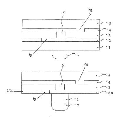
This process is illustrated in Fig. 1, wherein Fig. 1 a shows a solar cell
foil
comprising a temporary substrate 1 with on top of it a TCO 2a;2b, a PV layer
3,
a back electrode 4, and a permanent substrate 5. The interconnect 6 connects
the TCO layer to the back electrode 4. An etch resist cap 7 is provided on
'the
CA 02533331 2006-O1-19
WO 2005/015638 PCT/EP2004/008007
11
temporary substrate at the location of the interconnect. In Fig. 1b the same
system is shown after removing the temporary substrate except where' it is
provided with the etch resist cap. No etch resistant is present at the
location of
the front groove fg, thus no remainder of the temporary substrate (usually a
conductor such as aluminum) is present at the location of the front groove fg
to
cause short-circuit between separated TCO parts 2a and 2b.
A second embodiment, some steps of which are illustrated in Fig. 2, is a
process comprising the steps of:
~ providing an etchable temporary substrate
~ applying a front electrode of a transparent conductive oxide (TCO) onto the
fiemporary substrate
~ applying a photovoltaic layer (PV layer) onto the TCO layer and providing
grooves in the PV layer down to the TCO layer
~ applying a back electrode layer onto the PV layer and in the grooves present
in the PV layer so as to form an interconnect which connects the back
electrode layer to the TCO layer, and providing grooves in the back electrode
layer down to the PV layer or through the PV layer down to the TCO layer
~ applying a permanent carrier
~ in any one of the preceding steps providing an etch resist on the non-TCO
side of the temporary substrate at the location of the interconnect
~ selectively removing the temporary substrate where it is not covered with
etch resist
~ providing a groove through the TCO layer down to the PV layer or down to
the back electrode from the side of the TCO layer where the temporary
substrate was present.
Fig. 2a shows a solar cell foil comprising a temporary substrate 1 with on top
of
it a TCO 2, a PV layer 3, a back electrode 4, and a permanent substrate 5. The
interconnect 6 connects the TCO layer to the back electrode. An etch resist
cap
7 is .provided on the temporary substrate at the location of the interconnect.
In
CA 02533331 2006-O1-19
WO 2005/015638 PCT/EP2004/008007
12
Fig. 2b the same system is shown after removing the temporary substrate
except where it is provided with the etch resist cap. Further, a groove fg has
been established in the TCO layer so as to remove the short-circuit and
complete the series connection.
In a preferred version of this embodiment, protective strips of an insulating
material 8,9 are applied onto the PV layer before the back electrode is
applied.
The strips are applied at the location where in due course the grooves in the
back electrode and in the TCO layer will be obtained. These strips are
intended
to protect the underlying material during the provision of the grooves, e.g.,
through laser scribing. This embodiment is illustrated in Fig. 2c.
A third embodiment of the process according the invention comprises the
following steps:
75 ~ . providing an etchable temporary substrate
~ applying a front electrode of a transparent conductive oxide (TCO) onto the
temporary substrate
~ applying a photovoltaic layer (PV layer) onto the TCO layer and providing
grooves through the PV layer down to the TCO layer or through the TCO
layer down to the temporary substrate
~ applying a back electrode layer onto the PV layer and in the grooves in such
a way that inside the groove the back electrode is interconnected fio the
front
electrode, but the back electrodes on both sides of the groove are
electrically
insulated from each other
~ applying a permanent carrier
~ in any one of the preceding steps providing an etch resist on the non-TCO
side of the temporary substrate at the location of the interconnect
~ selectively removing the temporary substrate where it is not covered with
etch resist
CA 02533331 2006-O1-19
WO 2005/015638 PCT/EP2004/008007
13
~ providing a groove through the TCO layer down fio the PV layer or down to
the back electrode from the side of the TCO layer where the temporary
substrate was present.
Some steps of one embodiment of this process are illustrated in Fig. 3. Fig.
3a
shows a solar cell foil comprising a temporary substrate 1 with on top of it a
TCO 2, a PV layer 3, a back electrode 4, and a permanent substrate 5. A
groove g is present through the PV layer and through the TCO layer down to
the temporary substrate. An etch resist cap 7 is provided on the temporary
substrafie at the location of the groove through the PV layer and the TCO
layer.
In Fig. 3b the same system is shown after removing the temporary substrate
except where it is provided with the etch resist cap. The remaining part of
the
temporary substrate also funcfiions to connect the back electrode from one
side
of the groove to the TCO layer at the other side of the cell. Further, a
groove fg
has been established in the TCO layer so as to remove the short-circuit and
complefie the series connection. One of the features of this process is that
the
protective cap also functions as part of the interconnect. Therefore, for this
embodiment, the etchable temporary substrate should be conductive.
A second version of this embodiment is illustrated in Fig. 4. In this
embodiment,
the groove g in the PV layer does not extend through the TCO layer. In this
embodiment the protective cap does not function as part of the intercorinect,
so
it does not need to be conductive. Nevertheless the use of a conductive
temporary substrate is preferred.
A fourth embodiment of the presenfi invention comprises the following steps:
~ providing an etchable temporary substrate
~ applying a fronfi electrode of a transparent conductive oxide (TCO) onto the
temporary substrate
~ applying a photovoltaic (PV) layer onto the TCO, and providing a groove
through the PV layer and the TCO down to the temporary substrate, filling it
CA 02533331 2006-O1-19
WO 2005/015638 PCT/EP2004/008007
14
with an insulating material, optionally while applying a cap, and, if so
desired, applying an insulating strip, and establishing a (precursor of) a
conductive connection through the PV layer down to the TCO
~ applying a back electrode onto the PV layer
~ providing a groove in the back electrode down to the PV layer or, if
present,
down to the insulating strip
~ optionally applying a permanent carrier
~ in any one of the preceding steps providing an etch resist on the non-TCO
side of the temporary substrate at the location of the interconnect
~ selectively removing the temporary substrate where it is not covered with
etch resist.
This process is illustrated in Fig. 5. Fig. 5a shows a solar cell foil
comprising a
temporary substrate 1 with on top of it a TCO 2 and PV layer 3. A groove fg is
present through the PV layer and the TCO layer down to the temporary
substrate. This groove fg will be filled with an insulating material 8. A
further
groove 6 has been provided through the PV layer down to the TCO. This groove
6 wi(I form the basis for the interconnect, and may thus be seen as an
interconnect precursor. In Fig. 5b strips of insulating material 8 and 9 have
been
provided, one in the groove through the PV layer and the TCO down to the
temporary substrate, and one on the PV layer on the other side of the
interconnect precursor 6. In Fig. 5c back electrode 4 has been added, with a
groove bg on top of insulating strip 9. The interconnect is thus completed.
Additionally, an etch resist cap 7 is provided on the temporary subsfirate at
the
location of the interconnect. In Fig. 5d the same system is shown after
applying
a permanent carrier 5 and removing the temporary substrate except where it is
provided with the etch resist cap.
In this embodiment the (precursor of) the interconnect can be a groove which
on application of the back electrode is filled with back electrode material.
This is
the embodiment illustrated in' Fig. 5. Alternatively, although such a process
is
CA 02533331 2006-O1-19
WO 2005/015638 PCT/EP2004/008007
less favored at the moment, the groove can be filled with a conductive
material
in a separate step. Finally, if the PV layer is an amorphous Si layer, a
conductive connection can also be established by recystallising the amorphous
Si to form a conductive material. This last option is the least favored one.
5 A fifth embodiment of the present invention comprises the following steps:
a. providing a temporary substrate,
b. applying a transparent conductive oxide (TCO)
c. applying a photovoltaic (PV) layer on the TCO
d. if so desired, applying one or two insulating strips onto the PV layer
10 e. applying a back electrode onto the PV layer and, if they are present,
onto the insulating strips
f. if so desired, repairing shunts in the back electrode if no interconnect
has been established as yet
g. providing a groove in the back electrode down to the PV layer, or if it is
15 present, down to an insulating strip
h. if so desired, providing a permanent carrier
i. in any one of the preceding steps providing an etch resist on the non-
TCO side of the temporary substrate at the location of the interconnect
j. selectively removing the temporary substrate where it is not covered
with etch resist.
k. providing a groove from the side of the TCO through the TCO and,
optionally, through the PV layer down to the back electrode, or if it is
present, down to an insulating strip
I. if so desired, applying an encapsulant onto the TCO layer,
in which process a conductive connection through the PV layer is established
~ between steps f. and h, or
~ between steps c. and e.
Fig. 6 illustrates various products resulting from different embodiments of
this
process. These figures all show a show a solar cell foil comprising a TCO 2, a
PV layer 3, a back electrode 4, and a permanent substrate 5. The interconnect
6 connects the TCO layer to the back electrode. An etch resist cap 7 is
present
CA 02533331 2006-O1-19
WO 2005/015638 PCT/EP2004/008007
16
on the remainder of the temporary substrate 1 to protect the interconnect. The
advantage of the embodiment wherein the conductive connection is established
between steps f. and h. is that it is possible to effect shunt repair on the
assemblage of TCO layer, PV layer, and back electrode before the conductive
connection between the TCO layer and the back electrode is established.
The product of Fig. 6a is obtained by a process comprising the steps of:
a. providing a temporary substrate,
b. applying a transparent conductive oxide (TCO)
c. applying a photovoltaic (PV) layer onto the TCO
d. applying a back electrode onto the PV layer
e. if so desired, repairing shunts in the back electrode
f. 'providing a groove in the back electrode down to the PV layer, and
providing
an interconnect between the back electrode and the TCO layer
g. providing a permanent carrier
h. in any one of the preceding steps providing an etch resist on the non-TCO
side of the temporary substrate at the location of the interconnect
i. selectively removing the temporary substrate where it is not covered with
etch resist.
j. providing a groove from the side of the TCO through the TCO down to the
PV layer.
The system of Fig. 6b difFers from that of Fig. 6a in that two protective
strips of
an insulating material are applied onto the PV layer before application of the
back electrode. The groove in the back electrode is made from the back
electrode side down to the insulating strip. The groove fg from the TCO side
is
made through the TCO layer and the PV layer down to the other insulating
strip.
In the embodiments of Fig. 6a and 6b, the conductive connection between the
TCO .layer and the back electrode can be established in various ways. As the
back electrode is already present at the time the interconnect 6 is.
established,
the following options present themselves, If in this embodiment the PV layer
is
CA 02533331 2006-O1-19
WO 2005/015638 PCT/EP2004/008007
17
an amorphous Si layer, the conductive connection can be established by fusing
the back electrode and the amorphous Si layer using a laser. Alternatively, it
is
possible in these embodiments to first scribe a groove from the back electrode
side of the solar cell unit and establish or improve the interconnect by
filling the
groove with a conductive material. However, this option is less preferred.
The product of Fig. 6c differs from that of Fig. 6a in that the interconnect
interrupts the TCO layer instead of the back electrode of the solar cell foil.
It can
be obtained through a process comprising the following steps:
a. providing a temporary substrate,
b. applying a transparent conductive oxide (TCO)
c. applying a photovoltaic (PV) layer on the TCO
d. providing an interconnect through the PV layer and optionally through the
TCO layer
e. applying a back electrode onto the PV layer
f. providing a groove in the back electrode down to the PV layer
g. providing a permanent carrier
h. in any one of the preceding steps providing an etch resist on the non-TCO
side of the temporary substrate at the location of the interconnect
i. selectively removing the temporary substrate where it is not covered with
etch resist.
j. providing a groove from the side of the TCO through the TCO down to the
PV layer.
The system of Fig. 6d differs from that of Fig. 6c in that two protective
strips of
an insulating material are applied onto the PV layer before application of the
back electrode. The groove in the back electrode is made from the back
electrode side down to the insulating strip. The groove from the TCO side is
made through the TCO layer and the PV layer down to the other insulating
strip.
In this embodiment, the conductive connection between the TCO layer and the
back electrode can be established in various ways. If in this embodiment the
PV
layer is an amorphous Si layer, the conductive connection can be established
CA 02533331 2006-O1-19
WO 2005/015638 PCT/EP2004/008007
18
by recystallising the Si layer to form a conductive connection using a laser.
Alternatively, and preferably, it is possible in this embodiment to first
scribe a
groove through the PV layer and the TCO layer and establish the interconnect
by filling the groove with a conductive material.
The temporar)i substrate
The temporary substrate has to satisfy a number of conditions. It has to be
etchable, as has been explained above. It has to be sufficiently heat-
resistant to
be able to endure the conditions prevailing during the manufacture of the
solar
cell foil, more particularly during the deposition of the TCO and the PV
layer. It
has to be strong enough to be able to carry the solar cell foil during its
manufacture. It has to be easy to remove from the TCO layer without damaging
the latter. If it is intended to play a role in the interconnect, it has to be
sufficiently conductive. The person skilled in the art will be able to select
a
suitable temporary substrate within These guidelines.
The temporary substrate employed in the process according to the invention
preferably is a foil of a metal or a metal alloy. The principal reasons for
this are
that such foils exhibit good conductivity, generally are able to withstand
high
processing temperatures, are slow to evaporate, and are comparatively easy to
remove using known etching techniques. Another reason to choose a metal foil,
more particularly aluminium or copper, is that in the end the solar cell foil
has to
be provided with edge electrodes which have to connect the solar cell foil to
an
apparatus or the electricity grid. Remaining pieces of temporary substrate may
be used to this end, as a result of which there is no need for separate
provision
of the edge electrodes.
Suitable metals include steel, aluminium, copper, iron, nickel, silver, zinc,
molybdenum, chromium, and alloys or multi-layers thereof. For economic
reasons among others it is preferred to employ Fe, AI, Cu, or alloys thereof.
Given their performance (and taking into account the matter of cost)
aluminium,
iron, and copper are preferred most.
CA 02533331 2006-O1-19
WO 2005/015638 PCT/EP2004/008007
19
Suitable etchants and techniques for removing metals are known, and while
they differ per metal, the skilled person will be able to select the
appropriate
ones. Preferred etchants include acids (both Lewis and Br~nstedt acids). Thus
in the case of copper it is preferred to use FeCl3, nitric acid or sulphuric
acid.
Suitable etchants for aluminium are, e.g., NaOH, KOH, and mixtures of
phosphoric acid and nitric acid.
If copper, optionally prepared by way of electrodeposition, is used as
temporary
substrate, it is preferred to provide the copper, optionally via
electrodeposition,
with a non-reducing diffusion barrier layer, e.g., an anti-corrosion layer,
more
particularly zinc oxide. This is because copper may have the tendency to
diffuse
through the TCO layer in the PV layer. It is also possible to select a TCO
capable of preventing such diffusion, e.g., Sn02 or ZnO. The anti-diffusion
layers can be applied by means of for instance electrodeposition, or via
Physical Vapor Deposition (PVD) or via Chemical Vapor Deposition (CVD). The
anti-diffusion layer generally is . removed from the TCO together with the
temporary substrate.
For ease of removal, the temporary substrate preferably is as thin as
possible.
Of course, its thickness has to be such that other layers can be provided on
it
and it has to be able to hold these together, buff this generally does not
require it
to be more than 500 p,m (0.5 mm) thick. The thickness preferably is in the
range
of 1 to 200 p,m (0.2 mm). Depending on the modulus of elasticity, the minimum
thickness for a large number of materials will be 5 ~,m. Accordingly, a
thickness
of 5-150 p,m, more particularly 10-100 p,m, is preferred.
The TCO layer
Examples of suitable transparent conductive oxides (TCOs) are indium tin
oxide, zinc oxide, zinc oxide doped with aluminium, fluorine, gallium or
boron,
cadmium sulphide, cadmium oxide, tin oxide, and, most preferably, F-doped
Sn02. Said last-mentioned transparent electrode material is preferred, because
it can form a desired crystalline surface with a columnar light scattering
texture
CA 02533331 2006-O1-19
WO 2005/015638 PCT/EP2004/008007
when it is applied at a temperature above 400°C, preferably in the
range of 500
to 600°C, or after-treated at said temperature. It is precisely in the
case of this
TCO material that the use of a temporary substrate capable of withstanding
such a high temperature is extremely attractive. In addition, the material is
5 resistant to most etchants and has a better resistance to chemicals than the
much-used indium tin oxide. Also, it is far less costly.
The TCO can be applied by means of methods known in the field, e.g., by
means of Metal Organic Chemical Vapor Deposition (MOCVD), sputtering,
10 Atmospheric Pressure Chemical Vapor Deposition (APCVD), PECVD, spray
pyrolysis, evaporation (physical vapor deposition), electrodeposition,
electroiess
plating, screen printing, sol-gel processes, etc. or combinations of these
processes. It is preferred to apply and after-treat the TCO layer at a
temperature above 250°C, preferably above 400°C, more preferably
between
15 450 and 600°C, so that a TCO layer of the desired composition,
properties
and/or texture can be obtained:
The buffer layer
20 If so desired, a buffer layer may be present between the TCO layer and the
photovoltaic layer. The buffer layer is intended to protect the TCO layer from
the
conditions prevailing during the deposition of the PV layer. The nature of the
buffer layer will depend on the nature of the PV layer. Suitable buffer layers
for
the various PV layers are known in the art. For cadmium telluride CdS,
In(OH,S)
and Zn(OH,S) may be mentioned. If in the present specification mention is
made of depositing the PV layer on the TCO, a buffer layer may or may not be
present on said TCO.
The photovoltaic PV) lay
After application of the TCO layer the PV layer can be applied in an
appropriate
manner. It should be noted here that in the present description the term "PV
CA 02533331 2006-O1-19
WO 2005/015638 PCT/EP2004/008007
21
layer" or "photovoltaic layer" comprises the entire system of layers needed to
absorb the light and convert it into electricity. Suitable layer
configurations are
known, as are the methods for applying them. For the common general
knowledge in this field reference may be had to Yukinoro Kuwano, "Photovoltaic
Cells," Ullmann's Encyclopedia, VoLA20 (1992), 161 and "Solar Technology,"
Ullmann's Encyclopedia, VoI.A24 (1993), 369.
Various thin film semiconductor materials can be used in manufacturing the PV
layers. Examples are amorphous silicon (a-Si:H), microcrystalline silicon,
polycrystalline amorphous silicon carbide (a-SiC) and a-SiC:H, amorphous
silicon-germanium (a-SiGe), and a-SiGe:H. In addition, the PV layer in the
solar
cell foil according to the invention may comprise CIS (copper indium
diselenide,
CuInSe2), cadmium telluride (CdTe), CIGSS (Cu(In,Ga)(Se,S)), Cu(In,Ga)Se2,
ZnSe/CIS, ZnO/CIS, and/or Mo/CIS/CdS/ZnO, and dye sensitised solar cells.
The PV layer preferably is an amorphous silicon layer when the TCO comprises
a fluorine-doped tin oxide. In that case the PV layer will generally comprise
a
set, or a plurality of sets, of p-doped, intrinsic, and n-doped amorphous
silicon
layers, with the p-doped layers being situated on the side receiving the
incident
light.
In the a-Si-H embodiment the PV layer will at least comprise a p-doped
amorphous silicon layer (Si-p), an intrinsic amorphous silicon layer (Si-i),
and an
n-doped amorphous silicon layer (Si-n). It may be that onto the first set of p-
i-n
layers a second and further p-i-n layers are applied. Also, a plurality of
repetitive
p-i-n ("pinpinpin" or "pinpinpinpin") layers can be applied consecutively. By
stacking a plurality of p-i-n layers, the voltage per cell is raised and the
stability
of the system is enhanced. Light-induced degradation, the so-called Staebler-
Wronski effect, is diminished. Furthermore, the spectral response can be
optimized by choosing different band-gap materials in the various layers,
mainly
the i-layers, and particularly within the i-layers. The overall thickness of
the PV
layer, more particularly of all the a-Si layers together, will generally be of
the
order of 100 to 2,000 nm, more typically about 200 to 600 nm, and preferably
CA 02533331 2006-O1-19
WO 2005/015638 PCT/EP2004/008007
22
about 300 to 500 nm.
The back electrode
The back electrode in the thin film solar cell sheet according to the
invention
preferably serves both as reflector and as electrode. Generally, the back
electrode will have a thickness of about 50 to 500 nm, and it may comprise any
suitable material having light reflecting properties, preferably aluminium,
silver,
or a combination of layers of both, and making good ohmic contact with the
subjacent semiconductor layer. Preferably, it is possible to apply the metal
layers at a comparatively low temperature, say less than 250°C, by
means of,
e.g., electrodeposition, (in vacuo) physical vapor deposition or sputtering.
In the
case of silver, it is preferred to first apply an adhesion promoter layer.
Ti02, TiN,
ZnO, and chromium oxide are examples of suitable materials for an adhesion
promoter layer and have the advantage of also possessing reflecting properties
when applied in a suitable thickness, e.g., of 50-100 ~nm. The required back
electrode may be either transparent or opaque.
The permanent carrier
The solar cell foil is provided with a permanent carrier. For, otherwise the
toil
will be so thin that its fragility makes for difficult handling. The permanent
carrier
is applied on the back electrode. Suitable carrier layer materials include
films of
commercially available polymers, such as polyethylene terephthalate,
polyethylene 2,6-naphthalene dicarboxylate), polycarbonate, polyvinyl
chloride,
PVDF, PVDC, PPS, PES, PEEK, PEI or films of polymer having very good
properties such as aramid or polyimide films, but also, for example, metal
foils
onto which an insulating (dielectric) surFace layer may have been applied, or
compositions of plastics and reinforcing fibres and fillers. Polymeric "co-
extruded" films provided with a thermoplastic adhesive layer having a
softening
point below that of the substrate itself are preferred. If so desired, the co-
extruded film may be provided with an anti-diffusion layer of, e.g., polyester
CA 02533331 2006-O1-19
WO 2005/015638 PCT/EP2004/008007
23
(PET), copolyester or aluminium. Preferably, the carrier is a film or foil
with a
thickness of preferably 50 ~m to 10 mm. Preferred ranges are 75 pm to 3 mm
and 100 p,m to 300 ~,m. The bending stiffness of the carrier, defined within
the
context of this description as the product of the modulus of elasticity E in
N/mm2
and the thickness t to the power of three in mm (E x t3), preferably is higher
than
16x10-2 Nmm and will generally be lower than 15x106 Nmm. The carrier is
preferably suitable for use in a roll-to-roll process.
The carrier may comprise a structure as required for its final use. Thus the
substrate may comprise tiles, roofing sheets and elements, facade elements,
car and caravan roofs, etc. In general, however, preference is given to the
carrier being flexible. In that case a roll of solar cell foil is obtained
which is
ready for use and where sheets of the desired power and voltage can be cut off
the roll. These can then be incorporated into (hybrid) roof elements or be
applied onto tiles, roofing sheets, car and caravan roofs, etc., as desired.
If so desired, a top coat or surface layer may be provided on the TCO side of
the solar cell to protect the TCO from outside influences. Generally, the
surface
layer will be a polymer sheet (with cavities if so desired) or a polymer film.
The
surface layer is required to have a high transmission and for instance
comprises
the following materials: (per)fluorinated polymers, polycarbonate,
poly(methylmethacrylate), PET, PEN or any clear coating available, such as the
ones used in the car industry. If so desired, an additional anti-reflection or
anti-
fouling layer may be provided. Alternatively, if so desired, the entire solar
cell
may be incorporated into such an encapsulant.
The etch resist
The etch resist can be any material which can be applied to th.e temporary
substrate at the location of the interconnect which will protect the temporary
substrate from the action of the etchant. The skilled person can select
suitable
material by routine testing. Suitable etch resists include thermoplastic and
CA 02533331 2006-O1-19
WO 2005/015638 PCT/EP2004/008007
24
thermoset polyurethanes and poiyimides, thermoset polymers such as EP, UP,
VE, SI, (epoxy)resins, and acrylates, and thermoplastic polymers such as PVC,
PI, fluorpolymers, etc. The etch resist generally includes additives such as
photoinitiators or other hardeners, fillers, plastifiers, etc. The etch resist
may be
temporary, that is, it may be removed at some further stage of the process.
Alternatively, and preferably, the etch resist may be permanent.
The etch resist is suitably applied by vaporising or printing/writing.
Preferably,
the etch resist is applied by means of a printing process known as such.
Suitable printing processes include silk screening, roto screen printing, ink
jet
processes, flexgravure, etc. The color of the etch resist can be regulated by
the
incorporation of suitable pigments or dyes known to the skilled person.
Especia(fy for permanent etch resists, the presence of pigments and UV
stabilisers may be preferred.