Note: Descriptions are shown in the official language in which they were submitted.
CA 02533623 2006-01-24
WO 2005/025068 PCT/US2004/029451
TUNABLE OSCILLATOR
BACKGROUND
A voltage controlled oscillator (VCO) or oscillator is a
component that can be used to translate DC voltage into a
radio frequency (RF) voltage. The magnitude of the output
signal is dependent on the design of the VCO circuit and the
frequency of operation is determined by a resonator that
provides an input signal. Clock generation and clock recovery
circuits typically use VCOs within a phase locked loop (PLL)
to either generate a clock from an external reference or from
an incoming data stream. VCOs are therefore often critical to
the performance of PLLs. In turn, PLLs are essential
components in communication networking as the generated clock
signal is typically used to either transmit or recover the
underlying service information so that the information can be
used for its intended purpose. PLLs are particularly
important in wireless networks as they enable the
communications equipment to quickly lock-on to the carrier
frequency onto which communications are transmitted.
The popularity of mobile telephones has renewed interest
in and generated more attention to wireless architectures.
This popularity has further spawned renewed interest in the
design of low noise wideband oscillators. The recent
explosive growth in the new families of cellular telephones
and base stations using universal mobile telephone systems
(UMTS) has stirred a need for developing an ultra-low noise
oscillator with a fairly wide tuning range (e.g., octave-
band). The demands of wideband sources have generally
increased telescopically because of the explosive growth of
wireless communications. In particular, modern communication
systems are typically multi-band and multi-mode, therefore
requiring a wideband low noise source that preferably allows
simultaneous access to DCS 1800, PCS 1900 and WCDMA (wideband
CA 02533623 2006-01-24
WO 2005/025068 PCT/US2004/029451
2
code division multiple access) networks by a single wideband
vco.
The dynamic operating range and noise performance of a
VCO may limit or affect the performance of the PLL itself,
which in turn may affect the performance of the device in
which the PLL is employed, e.g., RF transceivers, cell phone,
modem.card, etc. Broadband tunability of VCOs represents one
of the more fundamental tradeoffs in the design of a VCO,
impacting both the technology and the topology used. The
dynamic time average quality factor (i.e., Q-factor) of the
resonator as well as the tuning diode noise contribution
affect the noise performance of a VCO. Furthermore, the
dynamic loaded Q is, in general, inversely proportional to the
operating frequency range of the VCO.
Despite the continuous improvement in VCO technology, low
phase noise typically remains a bottleneck and poses a
challenge to RF transceiver (transmitter - receivers) design.
This is typically considered due to the more demanding
parameters of the VCO design: low phase noise, low power
consumption and wide frequency tuning range.
In LC-resonator based VCOs, phase noise and power
consumption typically depend primarily on the time average
loaded Q-factor of the resonator circuit and the non-
linearities associated with the tuning network, which
typically employ varactors. The frequency tuning range is
determined by the usable capacitive tuning ratio of the
varactor and parasitic associated with the tuning network
because the parasitic deteriorates and limits the effective
tuning capability of the varactor at a high frequency. As the
loss-resistance of the tuning network (e.g., varactor and
resonator) determines the quality factor, special attention is
paid to the resistive behavior. The frequency range over
CA 02533623 2006-01-24
WO 2005/025068 PCT/US2004/029451
3
which a coupled resonator circuit can be tuned by means of the
tuning diode depends on the useful capacitance ratio of the
tuning diode and on the parallel and series capacitance
present in the circuit.
As the frequency for wireless communication shifts to
higher and higher frequency bands, generation of an ultra-low
noise, wideband, thermally stable and compact signal source at
a relatively low cost becomes more and more challenging due to
the frequency limitations of the active devices and broadband
tunability of the tuning diode. In the past, wide tuning
range and good phase noise performance were generally
considered to be opposing requirements due to the problem of
the controlling the loop parameters and the dynamic loaded Q
of the resonator over the range of wideband operation.
Typically, the phase noise of a microstrip line
resonator-based wideband VCO is -8OdBc/Hz @10 KHz (kilo-hertz)
for a frequency band of 1600 - 3200 MHz (mega hertz) operating
at 15V (volts), 45 mA (milli-ampere) A YIG resonator based
VCO offers wideband tunability with an external DC magnetic
field, but at a high price. In addition, the YIG resonator
based VCO is not amenable to integration in chip form.
Thus, there is a need for a wideband oscillator,
preferably having octave-band tunability, that offers a cost-
effective alternative to the YIG resonator based wideband VCO
in the frequency range of the L (0.95-1.5 GHz), S (1.7-
2.3 GHz), and C (4-6 GHz) bands.
SUMMARY OF THE INVENTION
In one aspect the present invention provides a topology
that supports wide-band tunability in a compact size, which is
amenable for implementation in integrated circuit form.
In another aspect, the present invention is a voltage
controlled oscillator. The voltage controlled oscillator in
CA 02533623 2006-01-24
WO 2005/025068 PCT/US2004/029451
4
accordance with this aspect of the present invention
preferably comprises a first device having first, second and
third terminals, a second device having first, second and
third terminals and circuitry comprising tunable coupled
resonator networks coupled to the second terminals of each of
the devices through a tuning voltage network. Preferably, the
voltage of the tuning network can be adjusted to tune an
output signal of the voltage controlled oscillator over an
octave frequency band.
Further in accordance with this aspect of the present
invention, a bias network is desirably coupled between the
first and third terminals of the first and second devices.
In accordance with this aspect of the present invention
the oscillator further desirably comprises a dynamically tuned
combiner network coupled between the third terminals of each
of the devices to combine signals present at the third
terminals into an output signal tunable over an operating
frequency range that is approximately twice the fundamental
frequency.
Preferably, the first and second devices each comprise
bipolar transistors, although field effect transistors (FET)
may also be employed.
It is also desirable that the tunable resonator networks
comprise a pair of micro-strip coupled resonators preferably
arranged in a horse-shoe configuration.
Further in accordance with this aspect of the present
invention, the voltage controlled oscillator is desirably
provided in the form of an integrated circuit.
In accordance with an additional aspect of the present
invention, a voltage controlled oscillator having octave band
tunability is provided. The oscillator preferably comprises a
first and a second three-terminal device; circuitry for' a
CA 02533623 2006-01-24
WO 2005/025068 PCT/US2004/029451
tunable phase coupling network coupled between respective
first terminals of the first device and second devices; and
circuitry for a dynamically tuned coupled resonator network
coupled to respective second terminals of the first and second
5 devices through a tuning voltage network. The voltage
controlled oscillator in accordance with this aspect of the
present invention may further desirably comprise a dynamically
tuned combiner network coupled between respective third
terminals of the first and second devices, wherein the
dynamically tuned combiner network combines signals present at
the third terminals of the first and second devices into an
output signal that is tunable over an octave frequency band.
Further in accordance with the aspect of the present
invention, the voltage of the tuning network may be adjusted
to tune the frequency of the output signal over the octave
frequency band. It is also desirable that the tunable
resonator network circuitry comprise a pair of micro-strip
coupled resonators arranged in a horse-shoe configuration.
In accordance with yet another aspect of the present
invention, an oscillator is provided. The oscillator
preferably comprises a transistor arranged in a parallel
emitter configuration and a resistance network coupled between
a first terminal and a second terminal of the transistor. The
resistance network is preferably capable of generating a
negative resistance. The oscillator also further desirably
includes a tuning voltage network coupled to the third
terminal of the transistor through a coupled resonator network
such that as the tuning voltage network is adjusted the
operating frequency of the oscillator is tuned over a
frequency band and the negative resistance generated is kept
substantially uniform over the frequency band.
In accordance with yet another aspect of the present
CA 02533623 2006-01-24
WO 2005/025068 PCT/US2004/029451
6
invention, a network communication device is desirably
provided. The network communication device preferably
comprises a phase lock loop for generating a clock signal used
to transmit or recover information communicated from or to the
device, wherein the phase lock loop includes a voltage
controlled oscillator for generating the clock signal. The
oscillator may further desirably comprise a first device
having first, second and third terminals; a second device
having first, second and third terminals; and circuitry
comprising tunable coupled resonator networks coupled to the
second terminals of each of the devices through a tuning
voltage network, wherein the dynamically tuned combiner
network combines signals present at the third terminals of the
first and second devices into an output signal that is tunable
over an octave frequency band.
In a further aspect, the present invention is a network
communication device. The device preferably comprises a phase
lock loop for generating a clock signal used to transmit or
receive information communicated from or to the device. The
phase lock loop preferably includes a voltage controlled
oscillator comprising a three terminal device arranged in a
parallel emitter configuration and a resistance network
coupled between a first terminal and a second terminal of the
device. The resistance network is preferably capable of
generating a negative resistance. The oscillator also further
desirably includes a tuning voltage network coupled to the
third terminal of the device through a coupled resonator
network such that as the tuning voltage network is adjusted
the operating frequency of the oscillator is tuned over a
frequency band and the negative resistance generated is kept
substantially uniform over the frequency band.
In accordance with this aspect of the present invention,
CA 02533623 2006-01-24
WO 2005/025068 PCT/US2004/029451
7
the voltage of the tuning network is preferably adjusted to
tune the frequency of the output signal over the octave
frequency band. It may further prove desirable in accordance
with this aspect of the present invention, if the device
comprises a wireless device including a cellular telephone or
a personal digital assistant.
Further still, in accordance with an additional aspect of
the invention, a voltage control oscillator comprising a first
three terminal device and a second three terminal device is
provided. Each three terminal device includes first, second
and third terminals. The first terminal of each of the
devices is preferably coupled together through a tunable phase
coupling network. Each of the second terminals of the devices
is coupled to respective dynamically tuned coupled-resonator
networks, which are preferably coupled together through a
tuning voltage network. Each of the third terminals of the
devices are coupled to each other through a bias network,
which is also coupled to the first terminal. A tunable output
signal at the fundamental frequency of the circuit is tapped
off each of the third terminals and preferably combined in a
dynamically-tuned combiner network. A tunable output signal
operating at twice the fundamental frequency of the circuit is
desirably obtained at the output of the dynamically-tuned
combiner network.
Further in accordance with this aspect of the present
invention, the circuit elements of the voltage controlled
oscillator are preferably selected such that the fundamental
frequency of operation of the circuit is tunable over 1000 MHz
to 2000 MHz. In accordance this preferred aspect, the tunable
output signal is tunable over a frequency range of 2000 MHz to
4000 MHz.
The three terminal devices may each preferably comprise
CA 02533623 2006-01-24
WO 2005/025068 PCT/US2004/029451
~
bipolar transmitters, although field effect transistors may
also be used.
In accordance with a further aspect of the present
invention, the circuit elements comprising the voltage control
oscillator are preferably selected and arranged in accordance
with FIG. 2. In yet another aspect, the present invention is
a voltage controlled oscillator preferably implemented in
accordance with the schematic diagram of FIG. 3. In yet
another aspect, the present invention is a voltage controlled
oscillator preferably implemented in accordance with the
schematic diagram of FIG. 4.
In another aspect, the present invention comprises a
voltage controlled oscillator having a three terminal bipolar
transistor in a parallel-emitter configuration. The base
terminal of the transistor is coupled to a wideband negative
resistance generating network, which is coupled across the
collector terminal of the transistor. A DC-bias and filtering
network is also coupled to the collector terminal. Circuitry
comprising a pair of coupled resonators and tuning diodes are
preferably coupled across the emitter terminal of the device
through a filtering and tuning voltage network. In accordance
with this aspect of the present invention, an output signal is
tapped from the collector terminal through a matching and
output network. Further in accordance with this aspect of the
present invention, the voltage controlled oscillator may be
preferably implemented in accordance with FIG. 8. In
addition, in accordance with this aspect of the present
invention, the voltage controlled oscillator is preferably
implemented or laid out in accordance with the schematic
diagram shown in FIG. 9.
In accordance with yet another aspect of the present
invention, a voltage controlled oscillator is provided. The
CA 02533623 2006-01-24
WO 2005/025068 PCT/US2004/029451
9
oscillator preferably comprises a first three terminal device
and a second three terminal device, each having a first, a
second, and a third terminal. The first terminals of the
devices are preferably coupled together through a tunable
phase coupling network. In addition, the second terminal of
each of the devices is coupled together through a tuning bias
voltage network and respective dynamically tuned coupled
resonator networks. The first and third terminals of each
device are coupled together through respective bias networks.
A tunable output operating at the fundamental frequency, based
on the values of the elements comprising the circuitry,
present at the collector of each of the devices is coupled
through a second harmonic combiner network. An output signal
tunable over a range twice the fundamental frequency of
operation results at the output of the combiner network. In a
most preferred embodiment the output signal is tunable over a
range comprising 3000 MHz to 6000 MHz. Further in accordance
with this embodiment, the voltage controlled oscillator is
implemented in accordance with the circuit diagram of FIG. 11.
In another aspect, the present invention is a method for
dynamically tuning an integrated coupled-resonator tuned
network, negative resistance generating network, phase-
coupling network and the second harmonic combiner network for
the realization of an ultra low noise octave band voltage
controlled oscillator. More particularly, the present
invention discloses an innovative approach of dynamic tuning
of a negative resistance-generating network, coupled-resonator
tuning diode network, and nth harmonic combiner network (n=2)
for ultra low noise octave band operation. This approach may
be implemented using any three terminal device such as bipolar
transistors and field-effect transistors or any other three
terminal device that may be implemented in the future.
CA 02533623 2006-01-24
WO 2005/025068 PCT/US2004/029451
In another aspect, the present invention offers a cost
effective and power efficient solution (5V, lOmA) to the
demand for a wideband oscillator, which is accomplished by
dynamically tuning the transistor's stability factors and
5 maintaining the time average loaded Q of the coupled resonator
over the desired tuning band.
In accordance with a further aspect of the present
invention, the coupled resonator and coupled oscillator
topology opens up the door to the high frequency ranges and
10 enables the realization of integrated silicon based systems
operating at higher frequencies during wideband operation.
Further in accordance with this aspect of the present
invention the design, fabrication, and performance of a
wideband voltage controlled oscillator that can satisfy the
present demand for a low noise, wide tuning range, less
harmonic content, manufacturing tolerance and miniaturization
is provided.
Furthermore, the freedom of selection of the frequency-
band of VCO implemented in accordance with the present
invention, its compact size, low cost, low power consumption,
and stability over the wide operating temperature range
provides a technology that is attractive for mobile
communication applications.
In accordance with a further aspect of the present
invention the effects that may limit the wideband tuning range
and development of unique topology, which can support octave-
band tunability are reduced.
A further aspect of the present invention is a compact,
power efficient, ultra low noise and low thermal drift
microwave octave-band VCO operating, for example, at 1600 MHz,
2000 MHz, and 3000 MHz with more than 100% tunable bandwidth.
The phase noise performance of a VCO implemented in accordance
CA 02533623 2006-01-24
WO 2005/025068 PCT/US2004/029451
11
with this aspect of the present invention is usually at least
-94dBc @ 10KHz, typically better than -100 dBc, for the
frequency band of 1600 - 3200 MHz, -90dBc/Hz@ 10KHz, typically
better than -95 dBc, for the frequency band of 2000 - 4000 MHz
and -85dBc/Hz@ 10KHz, typically better than -90 dBc, for the
frequency band of 3000 - 6000 MHz.
The present invention supports oscillations for more than
octave band tenability without degrading the loaded Q of the
circuit over the frequency band. A topology is desirably
designed to increase the loaded time average quality factor
over the frequency band by selecting an optimum coupling
factor of the micro-stripline coupled-resonator structure.
In accordance with yet another aspect of the present
invention, a system of coupled resonators is disclosed. The
disclosed system advantageously enhances the time average
loaded Q factor over the octave band. Application of this
approach results in an integrated dynamically tuned-
microstrip-coupled resonator based oscillator, which
significantly improves the phase noise performance depending
upon the coupling factor of the coupled resonator over the
wideband range.
In addition, the basic topology is extended to a system
of coupled voltage controlled oscillator for extending the
frequency of operation of the dynamically tuned coupled
resonator and this objective is accomplished by dynamically
coupling the oscillator over the entire band in such a way
that they mutually injection lock over the wideband (octave
band).
With regard to the state of the art of the push-push/N-
push oscillator, the present invention provides the general
implementation of an octave-band dynamically tuned tunable
coupled oscillator for an extended frequency range of
CA 02533623 2006-01-24
WO 2005/025068 PCT/US2004/029451
12
operation.
The topology and circuitry of the various aspects of the
present invention is desirably able to maintain the noise
performance over a wide temperature range (-400C to +850C)
throughout the octave-band of operation and the structure of
the layout remains substantially the same for other higher
frequency bands.
The foregoing and other aspects of the present invention
preferably include a topology, which provides constant
negative resistance over octave-band; a tuning arrangement for
wideband tunability without degrading the loaded Q of the
tuning network over the octave-band; a coupled-resonator
structure, which will support resonance over a octave-band;
the optimum size (Icmax/Idss) of the bipolar or FET for low
phase noise; a coupled-oscillator/N-Push approach for
improvement in phase noise; a second harmonic combiner
circuit; a dynamically tuned phase coupling network.
BRIEF DESCRIPTION OF THE DRAWINGS
FIG. 1 is a functional block diagram illustrating the
modules of a voltage controlled oscillator (VCO) in accordance
with an aspect of the present invention.
FIG. 2 is a schematic circuit diagram of VCO in
accordance with an aspect of the present invention.
FIG. 3 is a schematic of an integrated circuit comprising
a VCO in accordance with an aspect of the present invention.
FIG. 4 is a schematic of an integrated circuit comprising
a VCO in accordance with an aspect of the present invention.
FIG. 5 is a plot of RF-base currents of the sub-circuits
of FIG. 3 at the fundamental frequency of operation.
FIG. 6 shows a phase noise plot for a VCO over an octave-
band frequency range of 2 GHz to 4 GHz in accordance with an
aspect of the present invention.
CA 02533623 2006-01-24
WO 2005/025068 PCT/US2004/029451
13
FIG. 7 is a functional block diagram illustrating the
modules of a VCO in accordance with an aspect of the present
invention.
FIG. 8A is a schematic circuit diagram of VCO in
accordance with an aspect of the present invention.
FIG. 8B is a schematic circuit diagram of VCO in
accordance with an aspect of the present invention.
FIG. 9 is a schematic of an integrated circuit comprising
a VCO in accordance with an aspect of the present invention.
FIG. 10 illustrates a phase noise plot for the octave-
band frequency range of a VCO in accordance with an aspect of
the present invention.
FIG. 11 is a schematic circuit diagram of VCO in
accordance with an aspect of the present invention.
FIG. 12 is a plot of the RF-collector current of the
circuitry depicted in FIG. 12.
FIG. 13 is a plot of the RF-collector current of the
circuitry depicted in FIG. 12.
FIG. 14 illustrates a phase noise plot over an octave-
band frequency range of 1.6 GHz to 3.2 GHz.
DESCRIPTION OF THE PREFERRED EMBODIMENTS
In one aspect, the present invention relates to circuitry
for voltage controlled oscillators (VCOs). Preferably, such
oscillators have one or more of the following characteristics:
ultra-low phase noise performance, power efficient, low cost,
tunable with more than octave-band tunability and amenable to
integrated chip form.
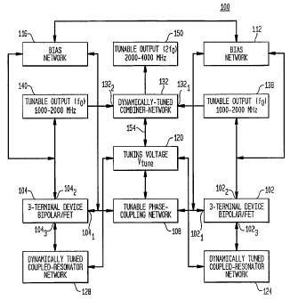
FIG. 1 illustratively depicts a functional block diagram
of the modules of a low noise octave-band voltage controlled
oscillator (VCO) 100 in accordance with an aspect of the
present invention. The VCO 100 is shown as operating in the
frequency range of 1000 - 2000 MHz/2000 - 4000 MHz (i.e., 1
CA 02533623 2007-12-12
= y =
WO 2005/025068 PCT/US2004/029451
14
GHz - 2 GHZ/2 GHz - 4Ghz), although the individual circuit
parameters, e.g.,resistor values, capacitor values, etc., may
be selected and arranged so that the circuit operates at a
different fundamental frequency and produces a tunable output
at both the fundamental frequency and second harmonic. In
addition, the topology shown in FIG. 1 may be extended, f rom a
push-push type configuration, such as 1 GHz - 2 GHz/2 GHz - 4
GHz/ 4 GHz - 8 GHz/ 8 GHz - 16 GHz, which allows the operating
frequency of the oscillator to be pxtended beyond the cut-off
frequency of the active device.
As FIG. 1 shows, the VCO/oscillator 100 includes a pair
of three terminal devices, 102 and 104, which are coupled
together through the other modules shown. More particularly,
each device 102 and' 104 includes three terminals, illustrated
as 1021, 1022 and 1023 and 1041, 1042 and 1043, respectively.
The first terminal 1021 of first device 102 is coupled to a
tunable phase coupling network 108 and bias network 112. The
tunable phase coupling network 108 is, also coupled to the
first terminal 1041 of the second device 104, which is also
coupled to a bias network 116 at terminal 1041. The tunable
phase coupling network 108 is also coupled to tuning voltage
.block 120. The tuning voltage block 120 is coupled to
dynamically tuned coupled-resonator networks, 124, 128, which
are respectively coupled to the third terminals 1023, 1043 of
each of the three terminal devices.
As discussed in U. S. Patent No. 7,196,591, the
terminal devices preferably comprise a bipolar transistor and
wherein the first, second and third terminals of the three
terminal device comprise either the collector, base and
emitter nodes of the bipolar transistor. On the other hand,
the three terminal device may comprise a field effect.
CA 02533623 2006-01-24
WO 2005/025068 PCT/US2004/029451
transistor wherein the first, second and third terminals of
the three terminal device either comprise the collector, base
and emitter nodes of the field effect transistor. As a
general matter, the three terminal device desirably includes
5 any three terminal device which is operable to provide a 180
degree phase shift between the first and second terminals.
The tuning voltage block 120 is further coupled to a
dynamically-tuned combiner network 132, which includes two
input ports, 1321 and 1322. Each of the input ports 1321 and
10 1322 accept input signals 138, 140 present at the second
terminals 1022 and 1042 of each of the devices. The
dynamically-tuned combiner network 132 combines the input
signals 138, 140 and produces a signal 150 operating at the
second harmonic of the input signals 138, 140.
15 The oscillator 100 preferably operates in the following
manner. The circuit elements comprising the various modules,
e.g., diodes, resistors, capacitors, resonators, etc., are
selected so that each of the three terminal devices 102, 104
oscillate at a fundamental frequency, fO. As the voltage
level of the tuning voltage module 120 is adjusted the
fundamental frequency of operation, fO, appearing as input
signals 138, 140 is tuned over the operating range of the
oscillator, e.g., preferably octave-band. These signals 138,
140 are then combined in the combiner network 132 to produce a
signal operating at twice the fundamental frequency, 2f0, and
that is dynamically tuned as the voltage level of the tuning
voltage module 120 is adjusted. A select portion of a signal
154 from the combiner network 132 is also fed back to the
tuning block 120. A portion of the signal 154 is then fed to
tunable phase coupling network 108 and used to dynamically
tune the phase of the output signals 138, 140, so that each of
these signals remain in phase during a tuning operation. In
CA 02533623 2006-01-24
WO 2005/025068 PCT/US2004/029451
16
addition, a portion of the signal 154 is also fed to each of
the dynamically-tuned coupled resonator networks 124, 128, so
that the frequency, fO, present at block 138 is at the same
frequency as the signal present at block 140. Accordingly, as
the tuning voltage, Vtune, is adjusted the frequency of the
signals, fO, present at each of the terminals 1022 and 1042
are tuned over the operating frequency band through the
coupled resonator networks 124, 128, while the phase coupling
network 108 keeps the two devices 102, 104 operating in an
anti-phase mode at the fundamental frequency, fO (e.g., push-
pull behavior), while the second harmonic, 2f0, interferes
constructively (e.g., push-push behavior) over the octave
band.
FIG. 2 depicts a schematic circuit diagram 200 of a VCO
designed in accordance with the principles of FIG. 1 in
accordance with an additional aspect of the present invention.
In particular, FIG. 2 illustrates a dynamically tuned coupled-
resonator network, dynamically tuned phase-coupling network
and dynamic tuned combiner network for octave-band 2-Push/
Push-Push operation. As one of ordinary skill in the art may
recognize, the rectangular blocks (e.g., A) in FIG> 2 (and the
other circuit diagrams that comprise this disclosure) are
transmission lines and coupling blocks (e.g., B or C) are
three port (T-connector) or four port connecters or couplers
that connected different circuit branches. Although FIG. 2
shows a 2-Push configuration the circuitry may be extended to
a N-Push configuration and provide a tunable signal at N times
the fundamental frequency of the sub-circuit's operation. The
sub-circuits comprise the respective bias networks, resonator
networks and three-terminal devices, which in this embodiment
are depicted as bipolar transistors although FETs may be used
also. The values of the individual circuit elements may
CA 02533623 2006-01-24
WO 2005/025068 PCT/US2004/029451
17
chosen so that the resulting output signal from the circuitry
operates in the L, S and C band and is tunable over a desired
frequency band, preferably octave-band. This configuration is
intended to overcome the limitations of the fixed frequency
operation of the push-push oscillator/N-push oscillator by
including a tuning and phase controlling network over the
desired frequency band (preferably octave-band).
FIG. 3 illustrates a schematic layout of an integrated
circuit (IC) 300 designed in accordance with the schematic
circuit diagram of FIG. 2 with the values of the various
circuit elements chosen such that the fundamental frequency is
tunable over the frequency range of 1000 MHz to 2000 MHz (1
GHz to 2 GHz) . In addition, the circuitry 300 also provides
an output that is tunable over the frequency range of 2000 MHz
to 4000 MHz (2 GHz to 4 GHz). As FIG. 3 shows the functional
diagram of FIG. 1 and the circuitry of FIG. 2 are amenable to
implementation as an integrated circuit. More particularly,
the integrated circuitry of FIG. 3 includes a printed
microstripline resonator and various discrete elements that
may be preferably implemented in Roger material.
FIG. 4 illustrates a schematic layout of another
integrated circuit 400 in accordance with the schematic
circuit diagram of FIG. 2. As in FIG. 3, the various
components of FIG. 2 are chosen such that the fundamental
frequency is tunable over the frequency range of 1 GHz to 2
GHz. In addition, the integrated circuit 400 also provides an
output that is tunable over the frequency range of 2 GHz to 4
GHz. In accordance with this aspect of the present invention,
the sub-circuits of each of the resonators are configured in a
push-push topology and each of the dynamically tuned coupled
resonators is provided in integrated circuit form. THe form
of the integrated circuit shown in FIG. 4 tends to be even
CA 02533623 2006-01-24
WO 2005/025068 PCT/US2004/029451
18
more compact than that shown in FIG. 3.
As FIGS. 3 and 4 demonstrate a VCO designed in accordance
with the foregoing aspects of the present invention may be
implemented in the form of a compact integrated circuit, such
as integrated circuits 300 and 400. The integrated circuits
300 and 400 may be advantageously mounted to a printed circuit
or wire board in wireless devices, such as cell phones or a
personal digital assistant, where space is at a premium. In
addition, these devices preferably include octave band
tunability, which allows for their deployment in applications
such as WCDMA.
FIG. 5 illustrates a plot 500 of the RF-base currents of
a voltage control oscillator of the type shown in FIGS. 3 or 4
at the fundamental frequency of operation. As FIG. 5 shows,
the RF-base currents are out of phase for the fundamental
frequency of the operation, 1000 - 2000 MHz.
FIG. 6 illustrates a typical phase noise plot 600 of an
oscillator implemented in accordance with the circuitry
illustrated in FIGS. 2, 3 or 4 for the octave-band frequency
range of 2000 - 4000 MHz. As FIG. 6 shows the phase noise of
the oscillator is approximately -90 dBc/Hz at 10 KHz over for
the frequency band of 2000 - 4000 MHz. However, the
integrated circuits 300, 400 typically provide better than -95
dBc/Hz at 10 KHz over for the frequency band of 2000 - 4000
MH z .
FIG. 7 is a functional block diagram illustrating the
modules of alow noise octave-band VCO 700 in accordance with
an additional aspect of the present invention. As shown in
FIG. 7, the VCO includes a three terminal device 710 that
includes terminals 7101, 7102 and 7103. The device 710 is
preferably configured as a parallel emitter transistor. The
first terminal 7101 is coupled to a DC-bias and filtering
CA 02533623 2006-01-24
WO 2005/025068 PCT/US2004/029451
19
network 716. The second terminal 7102 is coupled to a
wideband negative resistance network 720, which is also
coupled to the first terminal 7101 of the device 710. The
third terminal 7103 of the device 710 is coupled to a pair of
dynamically tuned coupled-resonator tuning diode networks 7261
and 7262 preferably through the parallel emitter of a three-
terminal bipolar transistor. In FIG. 7, the third terminal
7103 is shown twice on the device in order to simply the
diagram, yet while illustrating the parallel emitter
configuration. A filtering and tuning voltage network 730 is
coupled between the dynamically tuned coupled-resonator tuning
diode networks 7261 and 7262. The output signal of the VCO
700 is taken from a matching and output network 740 coupled to
the first terminal 7101 of the device.
In operation, the wideband negative resistance generating
network 720 maintains a constant resistance over the tuning
band of the oscillator 700. More particularly, the filtering
and tuning network 730 is tuned to adjust the oscillation
frequency of the device 710 through the coupled-resonator and
tuning diode 726. As tuning occurs the negative resistance
generating network 720 maintains uniform or constant negative
resistance over the tuning band. In this way, the phase noise
output of the oscillator may be maintained at a relatively
low, e.g., ultra-low, level.
FIG. 8A shows a schematic circuit diagram 800 of a
possible implementation of the functional diagram 700 of FIG.
7 in accordance with another aspect of the present invention.
As FIG. 8A shows, a filter and tuning bias network 810 is
integrated with a pair of coupled horse-shoe microstrip
resonator (8201 and 8202). The tuning network 810 and
negative resistance generating network 840 allows the VCO to
be tunable over more than an octave-band while maintaining a
CA 02533623 2006-01-24
WO 2005/025068 PCT/US2004/029451
uniform phase-noise performance through the band. The circuit
elements are preferably chosen to provide tunability over a
1600 - 3200 MHz frequency band. The circuit elements may also
be chosen to allow for tunability over other octave bands as
5 is discussed below.
FIG. 8B illustrates a schematic circuit diagram 850 of a
possible implementation of the functional diagram 700 of FIG.
7. The circuitry 850 of FIG. 8B includes a variable negative
resistance generating network 860, which is preferably coupled
10 to the base of a bipolar transistor 864. The transistor 864
is preferably arranged in a parallel emitter configuration
with a pair of dynamically tuned coupled-resonators 8681, 8682
coupled in parallel to the emitter. A filter and tuning bias
network 870 is coupled between the resonators 8681 and 8682 as
15 shown. The negative resistance generating network includes a
pair a variable capacitors that allow the negative resistance
to be variable over the tuning range. This in turns allows
the value of resistance provided by the network 860 to be
tunable over the tuning range of the oscillator.
20 FIG. 9 illustrates a schematic layout of an integrated
circuit 900 designed in accordance with the embodiment
illustrated FIG. 8A. The discrete elements and layout of the
integrated circuit of FIG. 9 may be chosen to allow for more
than octave band tunability over a 1.6 to 3.2 GHz operating
frequency range.
FIG. 10 shows a phase noise plot 1000 for the octave-band
frequency range of 1600 - 3200 MHz for the integrated circuit
900 of FIG. 9. As shown, the phase noise is approximately -
95dBc at 10 KHz, however the phase noise is typically better
than -100dBc at 10 KHz.
FIG. 11 depicts a schematic circuit diagram of a low
noise octave band VCO 1100 operating in the frequency range of
CA 02533623 2006-01-24
WO 2005/025068 PCT/US2004/029451
21
3000 - 6000 MHz in accordance with an additional aspect of the
present invention. The circuit diagram of FIG. 11 is
implemented in accordance with the functional diagram of the
FIG. 1, however the circuit elements comprising the various
modules are selected so as to provide a fundamental frequency
of operation of 1500 to 3000 MHz. Accordingly, the second
harmonic combiner network 1110 combines the signal at the
fundamental frequency produced at the collectors, 11301 and
11302, of the transistors to produce a signal that is tunable
over the frequency band of 3000 to 6000 MHz.
As FIG. 11 also shows, a dynamic tuning network 1134
which is integrated with coupled horse-shoe microstrip
resonators 11381 and 11382 is incorporated to get more than
octave band tunability while maintaining a uniform phase noise
performance throughout the band.
FIG. 12 is a plot 1200 of the RF-collector current of
both sub-circuits of FIG. 11, which are out of phase for the
fundamental frequency of operation, 1500 - 3000 MHz.
FIG. 13 is a plot 1300 of the RF-base currents of both
sub-circuits of FIG. 11, which are out of phase for the
fundamental (undesired frequency of the operation, 1500 - 3000
MHz. FIG. 14 shows a phase noise plot 1400 for octave-band
frequency range of 3000 - 6000 MHz for the circuitry shown in
FIG. 11.
A voltage controlled oscillator implemented in accordance
with the present invention may be employed in any number of
devices that are used to communicate on data, telephone,
cellular or, in general, communications network. Such devices
may include but are not limited to, for example, cellular
phones, personal digital assistants, modem cards, lap tops,
satellite telephones. As a general matter, the oscillator
circuitry shown in the various drawings and described above
CA 02533623 2006-01-24
WO 2005/025068 PCT/US2004/029451
22
may be employed in a PLL to either generate a clock signal
that may be used to transmit or recover information
transmitted or received over a network. In addition to
wireless networks, the circuitry of the present invention may
be employed in wired networks, satellite networks, etc.
Although the invention herein has been described with
reference to particular embodiments, it is to be understood
that these embodiments are merely illustrative of the
principles and applications of the present invention. It is
therefore to be understood that numerous modifications may be
made to the illustrative embodiments and that other
arrangements may be devised without departing from the spirit
and scope of the present invention as defined by the appended
claims.