Note: Descriptions are shown in the official language in which they were submitted.
CA 02533643 2009-02-12
1
"PROCESS FOR MANUFACTURING DEVICES WHICH REQUIRE A NON
EVAPORABLE GETTER MATERIAL FOR THEIR WORKING"
The present invention relates to a process for manufacturing devices which
require a non evaporable getter material for their working. The process is
particularly
suitable for being used in the processes for the manufacture of miniaturized
devices.
Non evaporable getter materials, also known as NEG, are capable of
reversibly sorbing hydrogen and irreversibly sorbing gases such as oxygen,
water,
carbon oxides and, in some cases, nitrogen.
The main NEG materials are transition metals such as titanium, zirconium,
vanadium, niobium, hafnium and tantalum, or alloys thereof (and in particular
titanium and zirconium) with one or more elements selected among the
transition
metals, Rare Earths and aluminum.
A first use of these materials is for keeping vacuum. The maintenance of
vacuum is required in very different applications, as for example in particle
accelerators, in X-rays generating tubes, in the flat displays of the field-
emission type
and in the evacuated jackets for thermal insulation, such as in thermal
vessels
(Thermos ), in Dewar bottles or in the pipes for oil extraction and transport.
NEG materials can be also employed to remove the above-mentioned gases
when traces thereof are present in other gases, generally noble gases. An
example is
the use in lamps, particularly fluorescent ones which are filled with noble
gases at
pressures of some tens of mbar, wherein the NEG material has the function of
removing traces of oxygen, water, hydrogen and other gases to keep a suitable
atmosphere for the operation of the lamp; another example of removal of traces
of the
above-mentioned gases by other gases is the purification of inert gases,
particularly
for applications in the microelectronic industry.
Another emerging application is the use of NEG materials in miniaturized
mechanical, electromechanical or optical devices. Since these devices are
industrially
important, and since the process of the invention is particularly suitable in
the
manufacturing processes of the same, in the following description reference
will be
particularly made to these devices and processes, but it is to be intended
that the
CA 02533643 2006-01-24
WO 2005/047558 PCT/IT2004/000615
-2-
present process has general applicability in each application wherein a NEG
material
is used.
The miniaturized mechanical or electromechanical devices are generally
known in the field with the English definition "Microelectromechanical
Systems", or
with the abbreviation MEMS, while the miniaturized devices of optical type are
known with the abbreviation MOEMS; for the sake of simplicity, however, the
definition MEMS will be used in the present text also with reference to MOEMS.
MEMS generally comprise an active device (the miniaturized mechanical,
ectromechanical or optical part) and ancillary parts, enclosed in a sealed
cavity;
electrical feedtliroughs assure the electrical supply to the device and the
transmission
of the signals from this toward the outside.
The last generation MEMS are manufactured through technologies derived
from the semiconductors industry, which comprise generally depositions on a
support of layers of a desired material and selective and localized chemical
attacks to
remove only predefined parts of a deposited layer or of the support, so as to
obtain
miniaturized structures and geometries which would not be obtainable through
traditional mechanics. Among the main types of MEMS, already used or in
development at present, it is possible to mention microaccelerometers, an
example of
which is disclosed in the patent US 5,952,572, used for example in the motor-
car
field to perceive collisions and thus to activate the air bag of the vehicle;
miniaturized mirrors, such as those disclosed in the patent US 5,155,778, used
in the
telecommunication systems in optical fiber; the arrays of miniaturized
mirrors, as
disclosed for example in the patent US 6,469,821, used in the formation of
images;
or microbolometers, that is, miniaturized detectors of infrared radiation, an
example
of which is disclosed in the patent US 6,252,229.
Several ways of manufactuuing MEMS have been proposed, but the most
common ones comprise the use of at least two planar supports made of glass or
quartz, ceramic material (e.g. silicon carbide) or semiconductor (silicon is
preferred),
whereon the different active and passive components of the MEMS are
constructed.
Commonly, upon one of the two supports (generally made of silicon) the active
parts
are constructed, for example the movable parts of a micromechanical device,
while a
CA 02533643 2006-01-24
WO 2005/047558 PCT/IT2004/000615
-3-
second support (which may be made up of glass or quartz, ceramic or
semiconductor
material) has essentially the funetion of closing the finished- device; the
electrical
feedthroughs for transferring signals between the inside and the outside of
the
MEMS may indifferently be obtained on any of the two planar supports.
Once all the components necessary for the operation of the MEMS have been
obtained on the two supports, said supports are fixed to each other, by
welding them
along a line which encloses the components of the device. The miniaturized
device is
thus sealed in a closed space and is mechanically and chemically protected
from the
outside. Numerous techniques, collectively knownn with the definition
"bonding",
may be used for the welding. A first possibility is the welding, simple or by
pressure
("pressure bonding"), wherein between the two supports it is interposed a
malleable
metal such as indium, lead or gold, and these are then melted and caused to
solidify
in the case of the simple welding, or pressed between the substrates in the
case of
pressure bonding: this technique, however, leads to weldings not completely
reliable
from the mechanical resistance standpoint. Another type of bonding is the
anodic
bonding (used especially in the case in which one of the two suppo'rts is made
up of
glass or quartz and the other of silicon), wherein between the two parts, kept
at a
temperature in the range from 300 to 500 C, is applied a potential difference
of
about 1000 V; in these conditions, there is a migration of positive ions from
the
support kept at the more positive potential (for example, sodium ions from the
glass)
toward the support kept at the more negative potential, and of negative ions
(for
example, oxygen from silicon) in the opposite direction; this migration of
material
between the two supports gives rise to the mutual welding thereof. A.nother
possible
teclui.ique is the eutectic bonding, wherein between the two supports is
interposed a
layer of a metal or alloy capable of forming an eutectic composition with the
material
of at least one of the two supports, so that with a suitable therrrmal
treatment a
localized melting in the welding area is caused. Finally, it would be possible
to use
the direct bonding, which comprises the localized melting of the material of
the
supports, but this process generally requires too high temperatures, for
example of
about 1000 C in the case of silicon, which may damage the component parts of
the
microdevice. Generally, all the types of bonding require a previous treatment
of the
CA 02533643 2006-01-24
WO 2005/047558 PCT/IT2004/000615
-4-
surfaces to be fixed to each other, because dirty surfaces endanger the
tightness of
the welding. These treatments are both of mechanical type (gas blowing or
mechanical washing with solid C02), aimed to remove particles present in the
welding area, and of chemical type, to eliminate the species (for example
oxides)
which alter the composition of the surface; the cllemical treatments generally
involve
washings of the support with acid or basic solutions, or combinations thereof
in
sequence.
All MEMS devices require a specific atmosphere for their working: for
example, the inner space of microbolometers must rigorously be under vacuum,
because traces of gases, if any, would give a convective contribution to the
heat
transfer in the system which would alter the measurement; the MEMS with moving
parts may be in vacuum or in inert atmosphere, but the humidity content of the
atmosphere must be controlled because water molecules present on the surface
of the
different parts which compose the microdevice may give rise to sticlcing
phenomena
or modify the friction between the stationary parts and the moving parts, thus
modifying the mechanical characteristics of the system. The control of the
inner
atmosphere of a MEMS is, consequently, extremely iinportant for the proper
working
thereof.
There are different mechanisms which tend to deteriorate the quality of the
inner atmosphere of a MEMS. First, the welding between the two supports,
although
properly accomplished, always leaves microscopic leaks which are channels for
the
passage of gases from the outside toward the inside of the cavity wherein the
device
is housed. Then, the same walls of the cavity and of all the inner parts of
the MEMS
release during time the gases adsorbed on their surface or dissolved inside
the
constituent material (phenomenon known as "outgassing"); this problem, common
to
all the devices under vacuum or containing a controlled atmosphere, is
particularly
felt in the case of MEMS, since these have a very high value of the ratio
between the
inner surface and the volume of the cavity. Even though the.,gas flow toward
the
inner space of a MEMS due to these two phenomena is small, it is an almost
constant
flow for the whole life of the device, so that in long periods of time, the
total effect
of alteration of the atmosphere with respect to the initial one, is important.
A third
CA 02533643 2009-02-12
phenomenon which considerably contributes to alter the atmosphere with respect
to
the optimal one takes place during the manufacturing process of the MEMS.
Particularly, the welding of the two supports requires always high
temperatures, from
some hundreds of degrees up to about 1000 C ; during this manufacturing step,
both
5 the components of the MEMS and the material added for the welding, release
big
amounts of gases which are mostly entrapped in the inner space of the device.
To obviate these problems, MEMS manufacturers use getter materials in the
device. However, differently from the traditional productions, wherein the
different
parts of a device are separately manufactured and finally assembled, in the
miniaturized productions, all components of a device are generally
manufactured in
series on a single support, or at most on two supports. This causes the
general
problem of the compatibility of each material deposited on a support with any
subsequent manufacturing steps ; when there is an incompatibility between a
material
and a process step, the material already deposited must be temporarily
protected, for
example with polymeric materials which are removed after the critical
operation has
been performed, but this obviously implies a slowing down and a complication
of the
process, with consequent increases of costs. The existence of the problem in
the
MEMS manufacture is acknowledged for example in patent US 6,252, 229, issued
June 26, 2001. In the case of getters, it is known that these materials have a
high
chemical reactivity with small molecules, apart from noble gases and in some
cases
nitrogen, and in the prior art it has been thought that the getter, once
deposited on a
support, has to be protected until the end of the manufacturing process, that
is until it
has to be exposed to the inner atmosphere of the cavity, already sealed, of
the MEMS.
In particular, at the state of the art, the treatment of a support whereon a
getter
material is already present with the acid or basic baths used for pre-treating
the
surfaces of the two supports before the welding operations, is considered
particularly
problematic.
This problem is the subject of patent application US2003/0138656, published
July 24, 2003, which discloses a method for manufacturing a support with a
getter
deposit, particularly for the use in MEMS. This document expressly
acknowledges
that the getter is a delicate component of the system, and must be temporarily
protected from the moment it is manufactured until the end of the
manufacturing
cycle of the MEMS. For this
CA 02533643 2006-01-24
WO 2005/047558 PCT/IT2004/000615
-6-
purpose the above mentioned application suggests to cover the getter deposit
with a
layer of a few nanometers of a noble metal, for example gold; this layer is
inert and
resistant to gases and to chemical reagents used in the different
manufacturing steps
of the MEMS, and thus it protects the getter deposit during said steps. In the
last step,
the bonding one, the temperature of the process causes the layer' of noble
metal to
diffuse into the underlying material, that is thus exposed to the atmosphere
in the
cavity of the MEMS.
Other patents disclose methods for avoiding the problem, or mention the
necessity of the presence of the getter in the MEMS without disclosing how to
integrate the formation of this component in the overall manufacturirig
process of the
final device.
The above mentioned patent US 6,252,229 proposes a manufacturing process
which comprises a double step bonding, a "pressure bonding" step along a
continue
closed line around the cavity to obtain the gastightness, and a second one,
for
example of anodic bonding, more external with respect to the first one, which
aims to
accoinplish a mechanically resistant welding of the two supports. According to
what
is disclosed in this document, with this process it would be possible to
eliminate the
getter in the cavity of the MEMS, but in this way the problem due to the
accumulation of gas in the cavity due to the outgassing of the inner surfaces
is not
solved; furthermore, the method is, in any case, coinplex and expensive,
requiring
two process steps for the bonding, which is normally accomplished with a
single
operation.
Patents US 6,621,134 and US 6,635,509 disclose processes wherein the MEMS
is rnanufactured starting from a single support, thus avoiding the problem of
the
bonding with the second support. These patents indicate the presence of the
getter
material; however, since the step of formation of the getter deposit takes
place almost
at the end of the process, said deposit is produced externally to the cavity,
covering
small openings obtained on the wall thereof: in these conditions the surface
of getter
material exposed to gases present in the cavity is extremely limited, whereby
the gas
sorbing efficacy of the getter during the life of the MEMS is also reduced.
The patent US 5,701,008 discloses a microbolometer , manufactured by
CA 02533643 2006-01-24
WO 2005/047558 PCT/IT2004/000615
-7-
assembling two supports and containing a getter material. As to the
manufacturing
process, this document refers to the previous patent US 5,433,639, whicli
relates to a
process for manufacturing an infrared radiation sensor of traditional type
(not a
MEMS), and wherein the different components are manufactured in parallel and
finally assembled; the process of US 5,433,639 is not directly applicable to
US
5,701,008, at least for what concerns the integration of the getter in the
cavity, and
therefore this last document does not give any information useful to solve the
problem.
Finally, patent US 6,590,850 mentions the general use of a getter in a MEMS
and discloses the location thereof, but it does not disclose the manufacturing
process
of the device and consequently does not mention how to introduce the getter
therein;
patent US 5,952,572 is even more vague, mentioning only the use of a getter, a
combination between titanium and an alloy Zr-V-Fe, without disclosing either
the
location of the getter in the cavity, and the less the step of introducing the
getter in
said cavity.
It is therefore clear that according to the present state of the art, the
integration
of the formation of a deposit of getter material in the manufacturing process
of a
MEMS is still an open problem, and that the solutions proposed up to now are
complicated aiid expensive.
The object of the present invention is to provide a process free from the
problems of the prior art for manufacturing devices which require for their
operation
a non. evaporable getter material.
Said object is achieved according to the present invention with a process
wherein:
- a deposit of non evaporable getter material is formed on a support;
- the support with the deposit of non evaporable getter material is then
treated with at least an acid or basic solution; and
- the so treated support is then introduced in the inner space of a device
whose operation requires the presence of a non evaporable getter material,
or is used to form at least a portion of the surface which defines the inner
space of said device, in such a way that said deposit is in contact with said
CA 02533643 2006-01-24
WO 2005/047558 PCT/IT2004/000615
-~-
space.
The invention is based on the inventors' acknowledgement that the chemical
treatments with acid or basic solutions (or combination in sequence thereof),
contrary
to what is commonly believed by those skilled in the art of getter materials,
do not
decrease the gas sorbing properties of the material, nor cause the loss of
particles
from the, deposit or its detaching fiom the support, so that a NEG material
may be
subjected to chemical treatments used for the manufacturing of some devices
wherein said material is required without having recourse to the measures of
the prior
art. Particularly, the inventors have detennined that the chemical treatments
with said
solutions not only do not cause the loss of particles from the NEG material
and do
not cause its detachment from the support, but in some cases allow also to
improve
the gas sorbing properties of the material.
The invention will be in the following described in detail with reference to
the
attached drawings, wherein:
- Figure 1 shows a part of a support on which a plurality of deposits of NEG
material are present, which may be used to manufacture a plurality of
devices containing said material;
- Figures 2 and 3 show in cross-section and in an extremely schematic way
two possible embodiments of devices containing a NEG material;
- Figures 4 and 5 show graphs representative of gas sorbing characteristics of
NEG deposits subjected to the process of the invention.
The invention may be used in all the cases in which the manufacturing process
of the device containing the NEG material comprises the treatment of the part
onto
which said material is deposited with acid or basic solutions. Moreover, the
process
of the invention may be used for the activation, at least partial, of the NEG
material;
the activation obtained through chemical way according to the present process
may
be thexl optionally followed by a further treatment of thermal activation.
As stated before, the invention is particularly suitable to be used in the
manufacturing processes of devices of the MEMS type wherein it is accomplished
the bonding of at least two supports, on one of which the getter is present.
The
supports used in these processes are slices of silicon, glass, quartz or
ceramic, called
CA 02533643 2006-01-24
WO 2005/047558 PCT/IT2004/000615
-9-
"wafer"*in the field, which have generally a thickness of about 0,2-2
millimeters and
diameters comprised between about 10 and 30 centimeters. On these wafer there
are
produced, with different tecluuques, the active parts of the MEMS device and
the
NEG deposits. From each wafer are generally obtained from some hundreds to
some
thousands devices. The NEG material may be deposited on the same support on
which is constructed (or from which is obtained) the active part of the
device, that
may be a moving part or a sensor of electromagnetic radiation. However, the
NEG
material is preferably deposited onto the other support, the one used to close
the
device (defined in the field "cap wafer"), because on this part there is more
available
space and thus it is possible to deposit a greater amount of getter, and
because in this
way there are no incompatibility problems between the deposition of the getter
and
the presence of the active structure. Figure 1 shows a part of a "cap wafer"
onto
which a plurality of NEG deposits are present: for the sake of ease, this cap
wafer is
represented witll some different areas thereof at different working steps, but
obviously in the real processes all the parts of its surface will be always in
the same
manufacturing step. Wafer 10 has a upper surface, 11, ideally divided into
areas 12,
12', ... (defined.in the figure by the broken lines), each of which will be
used to form
the closing element of a single MEMS; at the centre of each area 12, 12', ...,
in an
area 13, 13', ..., there is obtained, for example through anisotropic
cllemical attacks
known in the selniconductors field, a hollow 14, defined by lateral walls 15,
15', ...,
and by a bottom wall 16. On at least one of the walls 15, 15' or 16 the getter
deposit
17 is produced; preferably, said device is formed at least on the bottom wall
16,
which is the one that offers the greatest surface; furthermore, the most
common
technique of getter deposition in the MEMS manufacture is sputtering, and wall
16 is
the most convenient for said deposition being perpendicular to the arrival
direction of
the material according to this technique. The fmished cap wafer 10, wherein
all the
hollows 14 have internally a deposit 17 of getter material, is then placed
over the
support (not shown) on which the active components of the MEMS are
constructed,
in such a way that the hollows 14 define the cavity of the finished MEMS
device,
and that the walls 15, 15',... and 16 form, together with the surface of the
other
support, the walls of said cavity: The welding between the cap wafer 10 and
the
CA 02533643 2006-01-24
WO 2005/047558 PCT/IT2004/000615
-10-
support on which the active components of the MEMS are present is carried out-
in
the areas 18, that is the peripheric areas of each area 12, 12',...; the
welding may be
carried out by any known method, for example by anodic or eutectic bondiuig.
The getter material used may be any known NEG material, for example a metal
such as zirconium, titanium, tantalum, niobium, hafiiium or yttrium, or alloys
of at
least one of these metals (preferably zirconium or titanium) with one or more
elements selected among the transition metals, Rare Earths and alwninum.
As previously said, before bonding, areas 18 must be subjected to chemical
treatments for their cleaning. In the semiconductor industry there are
provided
numerous washing baths of the wafers, whose coinposition is standardized and
optimized to obtain specific effects; these baths comprise both acid and basic
solutions. Typical washing solutions are for example those named SCl and SC2,
wherein the wafer is immersed in sequence; the solution named SC1 is formed of
one
part (by volume) of ammonium hydroxide, one part of oxygenated water and five
parts of distilled water, and is usually used at temperatures comprised
between about
60 and 80 C; the solution named SC2 is formed of one part of hydrochloric
acid,
one part of oxygenated water and six parts of distilled water, and also in
this case it is
used at temperatures of about 60-80 C; after the washing with the solution
SC2, and
optionally also between the washing SCI and SC2, the support is generally
rinsed
with distilled water. Solution SCI accomplishes a gentle chemical attack of
the
surface of the wafer, removing organic contaminants and particles which
adheres to
said surface, while solution SC2 removes the metallic contaminants. Another
standard solution used in the field is a solution at 65% by weight of nitric
acid in
water, which is used at temperatures comprised between room temperature and
about
120 C, and also in this case is followed by rinsing with distilled water.
Other
standard washings are with aqueous solutions of hydrofluoric or sulphuric acid
at
differeiit concentrations; a broad description of the different washing
solutions used
in the field, and of their effects on substrates, is given in the book
"Handbook of
Semiconductor Manufacturing Technology", edited by Y. Nishi and R. Doering,
published in 2000 by Marcel Dekker, Inc. publisher (in particular, see pags.
87-104).
According to the process of the invention, during these steps of chemical
attack
CA 02533643 2006-01-24
WO 2005/047558 PCT/IT2004/000615
-11-
the whole surface 11 of the cap wafer, as well as the walls of the hollows 14
free of
the getter and the getter itself, are subjected to the same treatment, without
the
necessity of maskings for the temporary protection of the getter; this allows
to have a
simple, efficient and econoinic manufacturing process. Once the bonding has
been
carried out between the cap wafer 10 and the support on which the active
components of the MEMS device are constructed, the single devices may , be
separated by cutting along the broken lines 19, 19', ..., in figure 1.
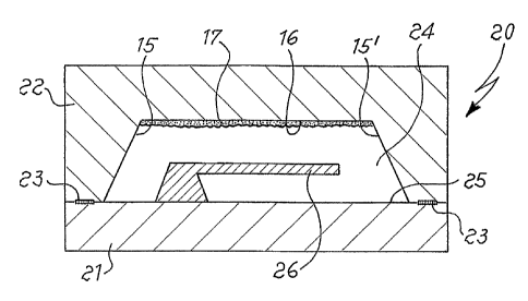
Figure 2 shows in section and in an extremely schematic way a MEMS device
which may be manufactured through the process of the invention. The device 20
is
formed by assembling a part 21 and a part 22, joined to each other through a
welding
23; each of these two parts originates from a support of bigger dimension, and
in
particular part 22 originates from a support of type 10 after it has been cut
along the
broken lines of figure 1; said cutting is preferably carried out after the
welding
operation of the two supports. Between the parts 21 and 22 there is a cavity
24,
which may be under vacuum or contain a controlled atmosphere; this cavity is
defined by surface 25 of part 21, and by walls 15, 15', ... and 16 described
with
reference to figure 1. Onto wall 16 of part 22 there is the deposit of getter
material
17; finally, in cavity 24 the active part, 26, of the MEMS device is housed.
For the
sake of simplicity there are not shown other elements which form the device,
such as
the electrical feedthroughs which connect part 26 with the outside of the
device.
Figure 3 shows another possible MEMS device, 30, produced with the process
of the invention. In this case, both the active part 31 and the getter deposit
32 are
formed on the same part of support 33, while part 34 acts, in this case,
simply as
closing element of cavity 35; this structure is, however, less preferable than
that of
figure 2, since, as already said, in this case the space available for the
getter deposit
32 is smaller (with a consequent reduced gas sorbing capacity) and the
production of
both deposit 32 and part 31 on a part 33 of the same support is more complex.
The formation of the getter deposit (17, 32) onto one of the two supports may
be carried out according to different techniques, for example by evaporation;
the
preferred technique is in any case sputtering, which is the technique most
widely
used in the industrial manufacture of miniaturized devices on planar supports,
and
CA 02533643 2006-01-24
WO 2005/047558 PCT/IT2004/000615
-12-
thus also of MEMS. The sputtering technique allows to obtain deposits with a
thickness from fractions of micrometers (micron, ,um) up to some tens of
micron,
which have an excellent adhesion to the substrate without loss of particles.
With this
technique it is also possible to control (at least within certain limits) the
morphology
of the deposit, optimizing it for the expected application; in the case of
getter
deposits; for example, it is preferable to have a columnar morphology, which
shows
a high specific surface (surface per unit of weight of the deposit). Moreover,
with
this technique it is possible to control to a high degree of precision also
the lateral
location of the deposit, ensuring that all deposits 17 or 32 are always in the
same
position in each device of type 20 or 30.
The getter deposit 17 or 32, even if it has already been activated during the
treatment with the cleaning chemical solutions of the surfaces of the two
supports,
undergoes a further activation during the bonding of said supports. As already
said,
all bonding operations imply the heating of the two supports at temperatures
of some
hundreds of degrees Celsius; at these temperatures all the components of the
MEMS
devices, under manufacture release gases; the bonding operation is usually
carried out
under pumping, just to eliminate these gases, but during bonding the two
supports are
necessarily very close, and in the final step of the bonding the cavity of the
device is
closed and thus the pumping from outside is ineffective. Having an active
getter
device in this step helps to get rid of the undesirable gases, potentially
harmful for
the application. The process of the invention, allowing to have an active
getter from
the very beginning of this operation, ensures a better cleaning of the inner
atmosphere of the device, because it increases the period of time in wliich
the getter
can play its action.
The invention will be further illustrated by the following examples.
EXAMPLE 1
In this example it is checked the compatibility of a support with a deposit of
getter material with the combined treatment with SCl and SC2 solutions.
On three silicon disks of 2.5 cm of diameter a 2 m thick deposit of an alloy
made up of zirconium, cobalt and Rare Earths is produced by sputtering; the
deposit
is produced starting from a target of alloy St 787, disclosed in the patent US
CA 02533643 2006-01-24
WO 2005/047558 PCT/IT2004/000615
-13-
5,961,750 in the name of the applicant. The first sample thus produced is not
treated
further, and constitutes the reference sample for this test. The second sample
is
immersed for 15 minutes in a bath of SC1 solution kept at 80 C, then taken
out,
rinsed with distilled water and dried with a flow of dry nitrogen. The- third
sample is
first iinmersed in the SC1 solution and then in the SC2 solution, for a period
of 15
minutes for each bath, then rinsed with distilled water and then dried with
dry
nitrogen.
The three samples so obtained are initially subjected to a visual analysis at
the
optic microscope to check the morphology of the deposit and the possible
detachinent from the support; this first examination confirms that after the
baths SC1
and SC2 there is no detachment of the deposit from the support, and that the
samples
treated with said baths do not lose particles.
Subsequently, the three samples are assembled in vacuum benches and
activated with a treatment under vacuum at 450 C for 45 minutes; afterwards
the
samples are allowed to cool at 25 C and their characteristics of hydrogen and
carbon
monoxide (CO) sorption are measured, according to the procedure defined in the
standard ASTM F 798-82, with a testing pressure of 10'4 Pa. The results of the
six
tests are reported in figure 4 (in double logaritlunic scale), as gas sorbing
rate, S
(measured in cc of gas sorbed per second and per square centimeter of deposit)
as a
function of the amount of gas sorbed, Q (measured in cc of gas sorbed
multiplied by
the pressure of measure in hectoPascal, hPa, per square centimeter of
deposit); in
particular, the graphs 1, 2 and 3 in figure 4 are referred to hydrogen
sorption
respectively on the reference sample, after the single treatment with SC1 and
after
the treatment with SC2, while the graphs 4-6 are referred to CO sorption on
the
reference sample, after the treatment with SC1 and after the treatment with
SC2.
EXAMPLE 2
In this example it is checked the compatibility of a deposit of getter
material on
a support with the coinbined treatment with aqueous solutions of nitric acid
at
different temperatures for different period of tirnes.
Four samples similar to those produced for example I are prepared. The first
one of these in not subjected to any treatment and constitutes the reference
sample;
CA 02533643 2006-01-24
WO 2005/047558 PCT/IT2004/000615
-14-
the second one is immersed for 30 minutes in an aqueous solution of HNO3 at
65%
by weight at room temperature; the third one is immersed in the same solution
for 10
minutes at 60 C; and the fourth one is immersed in the same solution for 10
minutes
at 120 C.
Also in this case the four samples, after possible rinsing and dtying with
nitrogen, are analyzed from the point of view of the detachment from support
and of
the loss of particles, confirming that the treatments in nitric acid do not
alter these
two parameters with respect to the reference sample.
The four samples are then subjected to hydrogen and carbon monoxide sorbing
tests as described in example 1. The results of the tests are reported in
figure 5, as
graphs from 7 to 10 for hydrogen sorption by, respectively, the samples from
the first
one to the fourth one as described; and graphs from 11 to 14 refer to CO
sorption by
the four samples (graphs 7 and 11 thus represent the properties of the
reference
samples in hydrogen and CO sorption, respectively).
As can be noted from the graphs reported in figure 4, while the SC1 treatment
worsens the sorbing characteristics of the getter films both for hydrogen and
CO, the
subsequent treatment with SC2 implies an improvement, increasing the hydrogen
sorption to a value that is about three times that of the reference sample,
and
increasing rate and capacity of CO sorption of about one order of magnitude.
All the
three treatments tested with nitric acid, instead, give rise to sorbing
characteristics of
both hydrogen and CO comparable one to the other, and also in this case
sensibly
better than those of the reference sample.