Note: Descriptions are shown in the official language in which they were submitted.
CA 02535537 2006-02-10
SF-1088
1
DESCRIPTION
TUBULAR REACTION VESSEL AND SILICON PRODUCTION PROCESS USING
THE SAME
FIELD OF THE INVENTION
The present invention relates to a novel reaction vessel
for producing silicon from a silicon deposition feedstock gas
containing a chlorosilane and hydrogen. More particularly,
the invention relates to a reaction vessel that permits stable
and efficient silicon production over extended periods and
enables reduction of by-products to an extremely low level.
The invention also relates to a silicon production process
using the reaction vessel.
BACKGROUND OF THE INVENTION
There are many known processes for producing
polycrystalline silicons used as semiconductors and
photovoltaic cell materials, and some processes are performed
in the industry.
One of such processes is the so-called Siemens process,
in which a silicon rod heated by energization to a silicon
deposition temperature is placed in a bell jar, and
trichlorosilane (SiHCl~, hereinafter TCS) or monosilane (SiH~)
CA 02535537 2006-02-10
SF-1088
2
together with a reducing gas such as hydrogen are brought into
contact with the rod to deposit silicon.
This process provides high-purity silicon and is
performed most commonly. Because of batchwise deposition,
however, the process has a problem of a very complicated
procedure including placement of the silicon rod as a seedbed,
energization heating, deposition, cooling and takeout of the
silicon rod, as well as bell jar washing.
To solve the above problem, the present applicant has
proposed a silicon production reactor capable of producing
silicon continuously and stably over extended periods (Patent
Document l, JP-A-2002-29726) . The reactor is structured such
that a silicon deposition feedstock gas is supplied into a
tubular reaction vessel resistant to temperatures in excess
of the melting point of silicon, the tubular reaction vessel
is heated to deposit silicon, and the deposited silicon is
molten and continually drips down from the lower end of the
tubular reaction vessel and is recovered.
This reactor is very advantageous in that the
conventional problems with the Siemens process are solved and
silicon is produced continually. However, it has been
revealed that the tubular reaction vessels disclosed in
Examples of Patent Document 1 that have a simple internal
structure circular or polygonal in cross section cause a
CA 02535537 2006-02-10
SF-1088
3
lowered reaction rate of the feedstock gas when the vessels
are scaled up without any modification for industrial-scale
production of more than several hundreds of tons of silicon
annually.
Furthermore, the scale-up tends to increase the
probability of generation of by-products such as silicon fine
powder and silane oligomers, resulting in lower silicon yields.
Moreover, the by-products often adhere to a reaction gas
discharge line to cause blockage. Therefore, improvements of
these problems have been desired.
Filling a reaction vessel with a filler or the like is
known as means for increasing the reaction efficiency of the
feedstock gas (Patent Document 2, JP-A-S59-16211'7).
However, the following problem is often encountered.
The silicon deposition reaction vessel is generally heated
inside by heat conduction from external heating means, and
therefore heat cannot reach deep into the filler layer. As
a result, a great temperature difference is caused within the
filler layer between the vicinity of the reaction vessel wall
and the vicinity of the filler layer central axis.
Sufficient heating to the vicinity of the central axis
is particularly difficult with a scaled-up large diameter
reaction vessel, even with the use of heating means such as
a high-frequency induction heating system or a dielectric
CA 02535537 2006-02-10
SF-1088
4
heating system which relatively facilitates deep heating, and
then, ultimately, a solid deposit clogs the filler layer. When
the heating output is increased to solve the above problem,
a vicinity of the heating means, for example the external wall
of the reaction vessel, is heated to an extremely high
temperature, so that the reaction vessel material is
remarkably deteriorated, leading to a new problem such as
difficult long-term operation.
Patent Document l: JP-A-2002-29726
Patent Document 2: JP-A-S59-162117
DISCLOSURE OF THE INVENTION
PROBLEMS TO BE SOLVED BY THE INVENTION
It is therefore an object of the present invention to
provide a reaction vessel whereby silicon produced can be
smoothly recovered dropwise without excessive thermal load on
constitutional parts of the reaction vessel, a silicon
deposition feedstock gas can be reacted efficiently even when
the reaction vessel is scaled up to industrial large-scale
equipment, generation of silicon fine powder and silane
oligomers can be suppressed, and industrial silicon production
can be performed over extended periods.
MEANS FOR SOLVING THE PROBLEMS
CA 02535537 2006-02-10
SF-1088
The present inventors studied earnestly to solve the
aforementioned problems. As a result, they have found that
a specific phenomenon attributed to operation conditions is
responsible for the lowered reaction rate of the silicon
5 deposition feedstock gas (hereinafter, feedstock gas) and
increased by-products encountered whenscaling up the reaction
vessel of Patent Document 1.
Even when the reaction vessel used in Patent Document
1 is scaled up, the Reynolds number indicates that the gas flow
is turbulent, thereby, the feedstock gas is supposed to be
sufficiently turbulent such that adequate contact efficiency
will be ensured. However, the present inventors have found
that when a low-temperature feedstock gas is flowed downward
into a reaction vessel whose wall (on which silicon will be
deposited) has a high temperature, particularly 1200°C or above,
a strong flow occurs near the deposition surface in the opposite
(upward) direction to the feedstock gas (downward). This
phenomenon becomes more marked as the temperature difference
between the wall and the gas increases.
Consequently, the upward flow blocks diffusion of the
feedstock gas to the deposition surface and the feedstock gas
reaction efficiency is just lowered, but, accidental local gas
turbulence brings part of the high-temperature upward flow
into contact with part of the low-temperature feedstock gas,
CA 02535537 2006-02-10
SF-1088
6
with formation of by-products. Moreover, the upward flow
reduces the possibility that the formed by-products will be
recontacted with the deposition surface, so that most of the
by-products are discharged from the reaction vessel.
The present inventors further studied to scale up the
Patent Document 1 reaction vessel while maintaining the
reaction efficiency and preventing occurrence of the
by-products. By providing the reaction vessel internal wall
with a flow resistance-increasing region, not only the
diffusion-blocking upward flow can be effectively diminished
but also the feedstock gas in the vicinity of the reaction
vessel central axis can be effectively mixed with the upward
flow. As a result, they have succeeded in achieving both
improvement of the feedstock gas reaction efficiency and
prevention of the by-products.
The present inventors have further found the following.
That is, the feedstock gas can be effectively contacted with
the deposition surface as described above, thereby, silicon
fine powder and the like can be recontacted with the deposition
surface and be incorporated in the deposit. Moreover, because
the feedstock gas supplied is uniformly heated to high
temperatures, the silane oligomer can be re-decomposed,
therefore, the by-products discharged from the reaction vessel
can be dramatically reduced.
CA 02535537 2006-02-10
SF-1088
7
The present inventors further studied and found that
reduction of temperature variation in the reaction vessel
internal wall, reduction of flow resistance of the feedstock
gas, and smooth drop of the silicon melt are achieved when the
shape, size and arrangement of the flow resistance-increasing
regions are adequately setting. The present invention has
been completed based on the aforesaid findings.
Furthermore, since the contact efficiency of the
feedstock gas with the reaction vessel wall is equalized
throughout the reaction vessel, the output distribution of
heating apparatus can also be leveled out, leading to reduced
operating cost.
Thus, a tubular reaction vessel according to the present
invention comprises a longitudinally-extending wall with a
space thereinside, wherein a silicon deposition feedstock gas
inflow opening and a deposited silicon discharge opening are
provided at an upper portion and a lower end portion
respectively, and a flow resistance-increasing region is
created on a wall surface of the tubular reaction vessel that
is contacted with a feedstock gas. According to the present
invention, the feedstock gas can be uniformly and sufficiently
heated by means of a very large deposition surface inside the
reaction vessel, so that the potential silicon production
capability of the feedstock gas can be fully educed while
CA 02535537 2006-02-10
SF-1088
8
preventing by-products, thereby, the present invention
achievesboth high silicon production efficiency and long-term
stable operation.
The flow resistance-increasing region is preferably at
least one of protrudent, concave and sloped regions . With the
thus-shaped flow resistance-increasing region, the silicon
deposition reaction vessel can be scaled up to industrial
large-scale equipment while permitting the silicon deposition
feedstock gas to react effectively and silicon to be mass
produced stably over a long term.
Preferably, the flow resistance-increasing region is a
protrusion provided in the tubular reaction vessel, and the
reaction vessel is reduced in thickness from the external wall
in the protrusion-provided area. Further, in a preferred
embodiment, the flow resistance-increasing region is a
protrusion provided in the tubular reaction vessel, and the
tubular reaction vessel is arranged to be heated by a high
frequency heating coil and includes means for reducing high
frequency energy from the high frequency heating coil in the
protrusion-provided area relative to the other area.
EFFECTS OF THE INVENTION
The invention enables effective reduction of the upward
flow by causing it to contact with the flow
CA 02535537 2006-02-10
SF-1088
9
resistance-increasing region on the internal wall of the
tubular reaction vessel to change the flow direction. The flow
resistance-increasing region also allows for effective mixing
of the feedstock gas with the upward flow in the vicinity of
the central axis of the tubular reaction vessel.
Consequently, the upward flow acting as a boundary layer
is eliminated, and the feedstock gas can contact with the
internal wall of the tubular reaction vessel with improved
efficiency and can be heated uniformly. Furthermore, the
feedstock gas can be effectively contacted with the deposition
surface and, even when silicon fine powder is generated, the
fine powder is recontacted with the deposited silicon surface
and is incorporated therein, in addition, the feedstock gas
can be heated uniformly to a high temperature, so that the
silane oligomer generated can be redecomposed, thereby, the
by-products discharged from the reaction vessel can be
dramatically reduced. Thus, improvement of the reaction
efficiency and prevention of by-products can be achieved.
PREFERRED EMBODIMENTS OF THE INVENTION
Hereinbelow, representative embodiments of the present
invention will be described with reference to the attached
drawings. However, the invention is not limited to the
illustrated embodiments.
CA 02535537 2006-02-10
SF-1088
Figs. 1 to 16 are schematic views illustrating
embodiments of tubular reaction vessels according to the
present invention.
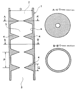
Fig. 1 is a schematic sectional view of a basic embodiment
S of a tubular reaction vessel according to the present invention.
(Fig. 1 is a vertical sectional view of the tubular reaction
vessel . )
In Fig. l, the numeral 1 denotes a tubular reaction vessel,
2 denotes a silicon deposition feedstock gas inflow opening,
10 3 denotes a deposited silicon discharge opening, 4 denotes a
flow resistance-increasing region, and 5 denotes a space
through which the silicon deposition feedstock gas is passed.
The tubular reaction vessel 1 shown in Fig. 1 has the silicon
deposition feedstock gas inflow opening 2 and the deposited
silicon discharge opening 3, and is provided with the flow
resistance-increasing regions 4 on a wall surface with which
the feedstock gas is contacted. In the figure, the section
along the line A-A' is of an area formed with the flow
resistance-increasing region at a right angle to the
longitudinal direction; the section along the line B-B' is of
an area without the flow resistance-increasing region.
Fig. 2 is a schematic sectional view showing another
embodiment of the tubular reaction vessel according to the
present invention. The numerals in Fig. 2 indicate the same
CA 02535537 2006-02-10
SF-1088
11
items as in Fig. 1.
The flow resistance-increasing regions shown in Fig. 1
are ring-shaped protrusions triangular in cross section,
provided on the internal wall of the tubular reaction vessel
(hereinbelow, the ring-shaped protrusionsontheinternal wall
of the tubular reaction vessel will be referred to as orifices ) .
In Fig. 2, the orifices rectangular in cross section are
provided on the internal wall.
One or more flow resistance-increasing regions 4 will
be suitably provided depending on the size of the tubular
reaction vessel. The intervals at which the flow
resistance-increasing regions are provided may be regular as
shown in Figs. 1 and 2, or may be specifically determined
irregular intervals . In Figs . 1 and 2, the orifice height is
represented by H, the skirt width by Q, and the orifice interval
by P. A detailed description will be given below.
Tubular reaction vessel
The tubular reaction vessel 1 comprises a
longitudinally-extending wall with a space thereinside. The
reaction vessel has a silicon deposition feedstock gas inflow
opening and a deposited silicon discharge opening at an upper
portion and a lower end portion respectively, and further has
a flow resistance-increasing region on a wall surface to be
contacted with the feedstock gas. The shape of the reaction
CA 02535537 2006-02-10
SF-1088
12
vessel is not particularly limited provided that a silicon
deposition feedstock gas is supplied through the upper silicon
deposition feedstock gas inflow opening 2, that silicon is
deposited and molten on a heated surface of the reaction vessel
wall (a) facing a space 5, and that an opening (discharge
opening 3) is formed at a lower end portion for allowing silicon
to drip down by gravity from the vessel.
The cross-sectional shape of the tubular reaction vessel
1 is not particularly limited. For example, the transverse
cross section (along the line B-B' ) of the space 5 is basically
circular as shown in Fig. 1 or 2, and may be any shapes such
as polygonal shapes including triangular and square shapes.
In another embodiment, the transverse cross section of
the space 5 may be slit-shaped as illustrated in Fig. 13.
Examples of the slit shapes in transverse cross section of the
space 5 of the reaction vessel 1 include the rectangular shape
as shown in Fig. 13 and, although not shown, corner-rounded
polygonal shape, elliptical shape, C-shaped curved
rectangular shape, rhomboid shape, one side open square box
shape(II shape), L shape, T shape, cross shape, star shape, S
shape and scroll shape.
A further example of the slit shapes is a continuous
circular slit shape as shown in Fig. 14.
One of the main characteristics of the reaction vessel
CA 02535537 2006-02-10
SF-1088
13
of the invention is a scale-up property. That is, the reaction
vessel of the invention can be scaled up from a laboratory-scale
small vessel to a substantially analogous but industrial
large-scale vessel, so as to provide reaction results
surprisingly similar to laboratory results.
The reaction vessel may be produced by know molding
methods . The reaction vessel may consist of an integral body,
or two or more parts joined together. A large-scale reaction
vessel for industrial use is preferably constructed by
connecting structural parts of the tubular reaction vessel,
each of which is 1.5 m long at maximum, to obtain as uniform
mechanical properties as possible of the tubular reaction
vessel material. Connection of the parts may be flange
connection. Preferably, the tubular reaction vessels are
ditched to create a screw, and are connected together by means
of the screws. In the case of the screw connection, it is
preferred that the inner surface of the tubular reaction vessel
is free from steps . When steps are present, silicon is locally
deposited thereon from which breakage of the reaction vessel
possibly takes place.
Specifically, the diameter D of the tubular reaction
vessel is not particularly limited and may be selected
appropriately depending on the silicon production scale,
within production conditions of the structural material. The
CA 02535537 2006-02-10
SF-1088
14
length L of the reaction vessel may be extended as required
by screw connecting reaction vessel parts. The length to
diameter ratio (L/D) of the tubular reaction vessel, although
variable depending on arrangement of the flow
resistance-increasing regions, is in the range of 1 to 30, and
preferably 3 to 20 in order to achieve a sufficient reaction
rate of the feedstock gas and a good silicon yield.
The diameter D of the tubular reaction vessel may be
constant at any points as shown in Figs. 1 to 16. It is also
possible, although not shown, that the diameters differ from
place to place. In the case of the slit shape, the width may
be constant or varied relative to the longitudinal direction
(direction L) of the reaction vessel.
The thickness of the tubular reaction vessel is not
particularly limited, and will be such that the reaction vessel
will have strength enough to support its own weight. That is,
the thickness does not need to be unnecessarily large and will
suitably range from 5 to 100 mm, and preferably from 10 to 50
mm.
In order that silicon can be appropriately discharged,
the silicon discharge opening 3 of the reaction vessel 1 may
have a horizontal peripheral edge. It is also appropriate that
the peripheral edge is sloped or waved. In a preferred
embodiment, the discharge opening 3 is tapered, with the
CA 02535537 2006-02-10
SF-1088
thickness being gradually reduced toward the tip, so that the
silicon melt can drip down clear from the discharge opening
3.
The tubular reaction vessel 1 is heated to above the
5 melting point of silicon and the inside of the vessel is
contacted with chlorosilane and the silicon melt. To enable
long-term stable production of silicon, the vessel is
preferably made of a material highly resistant to these
temperature conditions and contact.
10 Such materials include single and composite materials
of carbon materials such as graphite, pyrolytic carbon and
carbon fiber-reinforced carbon composite materials, and
ceramic materials such as silicon carbide (5iC), silicon
nitride (Si3N~) , boron nitride (BN) and aluminum nitride (A1N) .
15 Of these materials, isotropic graphite is preferable to
constitute the wall (a) of the reaction vessel. To reduce
contamination of the deposited silicon, the vessel is
preferably coated with pyrolytic carbon, Si3N9 or SiC at least
in the area that is contacted with the silicon melt.
Flow resistance-increasing region
The flow resistance-increasing region is provided to
effectively diminish the upward flow which is a layer
inhibiting diffusion in the tubular reaction vessel and to
effectively mix the feedstock gas in the vicinity of the vessel
CA 02535537 2006-02-10
SF-1088
16
central axis with the upward flow. The provision of the flow
resistance-increasing region achieves both improved reaction
rate of the feedstock gas and by-products prevention. The
feedstock gas reaction rate is defined as a conversion ratio
of the feedstock gas relative to any substance converted
therefrom while the feedstock gas is supplied into the space
5 of the tubular reaction vessel 1 and is discharged from the
space 5. The silicon yield mentioned later is defined as a
conversion ratio of any substance converted from the feedstock
gas, relative to the silicon produced.
Specifically, the flow resistance-increasing region 4
may be a protrusion, a concave or a slope, as described below.
1) Protrusion
Protrusion is the most preferable embodiment of the flow
resistance-increasing region. The protrusion means a raised
portion of the tubular reaction vessel wall protrudent toward
the space 5.
In a most preferred embodiment, the protrusion is a
ring-shaped protrusion (orifice) circulating on the internal
wall of the tubular reaction vessel, as illustrated in the cross
section along the line A-A' . The protrusion will be described
in detail hereinbelow based on this typical embodiment
orifice.
The cross sectional shape of the orifice in a vertical
CA 02535537 2006-02-10
SF-1088
17
direction (longitudinal direction of the tubular reaction
vessel) is not particularly limited. The orifice in cross
section may be triangle as illustrated in Fig. l, rectangle
(oblong) as illustrated in Fig. 2, polygon (not shown), or a
top-curved protrusion (not shown).
More preferably, the orifice has a cross sectional shape
such that gas stagnation will be less and the silicon melt will
flow down smoothly.
The orifice is more preferably triangle in cross section
as illustrated in Fig. 1 because the flow will be difficult
when the protrusion has corners. The triangular orifice may
have a regular shape such as right-angled triangle or isosceles
triangle, or may have an irregular triangle shape. Most
preferably, in order that the orifice can effectively function
as the flow resistance-increasing region and that the gas
stagnation andaccompanying temperature rise in the downstream
of the orifice can be prevented, the flow
resistance-increasing region has a triangular cross section
that is sloped more gently in the downstream gas flow side than
in the upstream side. That is, as shown in Fig. 3, the exterior
angle of the triangle and the wall surface is desirably more
obtuse in the downstream side of the gas flow than in the
upstream side. In the vertical cross section, although the
protrusion and the tubular reaction vessel may have an angled
CA 02535537 2006-02-10
SF-1088
18
contact point, the contact point is more preferably curved as
shown in Fig. 3, with designation R (partially semicircle) in
accordance with JIS, so that the silicon melt having a high
surface tension can flow down more smoothly. R is preferably
in the range of about 5 to 10.
The orifice opening through which the gas is passed may
be circular as shown in Figs . 1 and 2 or, although not shown,
elliptical or polygonal.
The orifice opening through which the gas is passed is
preferably positioned exactly in the center of the tubular
reaction vessel 1 as shown in Figs. 1 and 2. Namely, the center
of the orifice opening preferably meets the central axis of
the gas passageway of the tubular reaction vessel. Although
not shown, an eccentric opening may be employable. The
eccentric opening may cause nonuniform heating, and therefore
the opening is desirably positioned on the central axis of the
gas passageway.
The orifice blocks part of the gas passageway, so that
the gas flow is locally accelerated. As a result, the
occurrence of the upward flow is prevented and the feedstock
gas can be efficiently mixed with the upward flow in the
downstream of the orifice.
The protrusion height H from the tubular reaction vessel
internal wall to the orifice tip will be preferably such that
CA 02535537 2006-02-10
SF-1088
19
the area in which the gas passageway is blocked by the
protrusion is 10 to 950, more preferably 30 to 950, and
optimally 50 to 95 0 of the cross sectional area of the tubular
reaction vessel 1 in the wall provided with the protrusion.
When this condition is satisfied, the upward flow being a layer
inhibiting diffusion of the feedstock gas can be effectively
reduced and the feedstock gas in the vicinity of the tubular
reaction vessel central axis can be effectively mixed with the
upward flow. Thus, the reaction efficiency of the feedstock
gas can be improved and the by-products can be prevented.
The orifice skirt width Q (shown in Figs. 1 and 2) is
preferably 50 to 600 0, and more preferably 100 to 400 o relative
to the protrusion height H. Too large a skirt width Q reduces
the effect of the protrusion, and too small a skirt width
possibly leads to lowered protrusion strength.
The number of orifices to be provided is determined
appropriately depending on the size of the tubular reaction
vessel, the flow speed and rate of the feedstock gas, and
desired reaction results. One or more orifices, preferably
a plurality of orifices are provided. In an optimum embodiment,
the number of orifices ranges from 3 to 10.
A plurality of orifices are preferably provided at
intervals P that are 100 to 5000, and more preferably 200 to
400 o relative to the inner diameter D of the tubular reaction
CA 02535537 2006-02-10
SF-1088
vessel 1. When the intervals P are too small, the protrusions
will not produce sufficient effects. Too large intervals
reduce the probability that the gas will contact with the wall
surface. When the orifices are triangular or curved in cross
5 section, the interval P is a distance between peaks of the
height H as shown in Fig. 2. When the cross sectional shape
is quadrangular or polygonal with a flat top, the interval P
is a distance between central points of the flat areas as shown
in Fig. 1.
10 Next, embodiments of the protrusion arrangement will be
described based on various combinations of the orifice height
H, skirt width Q and intervals P.
Basically, the protrusion height H, skirt width Q and
intervals P are regular as illustrated in Figs. 1 and 2.
15 In another embodiment, the skirt width Q alone is changed
as shown in Fig. 4, in which the more downstream of the gas
passageway the protrusion, the greater the skirt width Q.
Although not shown, the embodiment of Fig. 4 may be turned
upside down so that the skirt width Q narrows toward the
20 downstream of the gas passageway.
In a further embodiment, the protrusion height H may be
changed (be sequentially increased) as shown in Fig. 5.
Although not shown, the embodiment of Fig. 5 may be turned
upside down (so that H is sequentially decreased) . In a still
CA 02535537 2006-02-10
SF-1088
21
further embodiment, the intervals P alone may be changed as
shown in Fig. 6. Although not shown, the embodiment of Fig.
6 may be turned upside down.
In a yet further embodiment, various embodiments of the
protrusion height H, skirt width Q and interval P may be
arbitrarily combined. For example, the protrusion height H,
the skirt width Q and the intervals P may be gradually increased
as shown in Fig. 7.
The heating energy from heating means, for example high
frequency wave in the case of high-frequency heating, tends
to be concentrated to the orifice-provided regions, and
therefore the internal temperature is often raised, possibly
resulting in breakage of the tubular reaction vessel.
Accordingly, it is desirable that the thickness of the reaction
vessel is reduced by concaving the external wall in the
orifice-provided region to prevent overheating.
For example, the external wall is desirably concaved
semicircularly as shown in Fig. 26. The concave depth is not
particularly limited. For example, the external wall may be
concaved to a depth such that the distance from the bottom of
the semicircular concave to the orifice top is equal to the
thickness of the tubular reaction vessel . There is no problem
if the concave depth is smaller. Although the semicircular
concave will be appropriate, the concave may be semi-spindle
CA 02535537 2006-02-10
SF-1088
22
shaped so as to reduce the thickness of the reaction vessel
wall near the lower surface of the orifice because heat is most
often concentrated to the orifice' s lower surface to overheat
the area. The reduction thickness of the reaction vessel wall
from the external wall prevents heat from being concentrated
to the orifice, so that the overheating the inside of the
orifice can be prevented, leading to enhanced durability of
the tubular reaction vessel.
In an optimum embodiment of the protrusion arrangement,
the aforementioned various provision embodiments will be
appropriately selected and adjusted such that the silicon
deposition efficiency will be most enhanced depending on the
reaction vessel diameter or the gas feeding rate.
That is, it is an industrial advantage of the present
invention that a gas heating process in the tubular reaction
vessel 1 may be designed arbitrarily by appropriately
selecting and adjusting the aforesaid provision embodiments
of the flow resistance-increasing regions. Namely, the
present invention achieves the following:
the distribution of the heating energy to the tubular
reaction vessel I can be equalized to reduce operating costs,
and most importantly, the invention provides means
whereby a silicon deposition process, in which the gas heating
temperature and the consumption by reaction of the feedstock
CA 02535537 2006-02-10
SF-1088
23
gas continually change, can be designed such that the maximum
efficiency will be achieved in all the areas of the deposition
(wall) surface of the tubular reaction vessel l,
and ultimately the entire deposition surface can be
utilized with maximum efficiency.
As described above, the reaction vessel that is
circumferentially continuous circular slit in horizontal
cross section consists of an outer tube and an inner tube. In
the thus-shaped reaction vessel, the flow
resistance-increasing regions may be favorably provided on
both the external wall of the inner tube and the internal wall
of the outer tube as shown in Fig. 15; or may be formed only
on the external wall of the inner tube as shown in Fig. 16;
or, although not shown, may be formed only on the internal wall
of the outer tube.
In further embodiments of the protrusions, protrusions
that do not circulate on the internal wall (sometimes referred
to as baffle plates) may be provided as illustrated in Figs.
8 and 9. The protrusions having these shapes are capable of
the same effects as those shown in Fig. 1. In a modified
embodiment of Fig. 9, although not shown, the protrusions may
be inclined like gas turbine blades to swirl the stream of the
silicon deposition feedstock gas in the reaction vessel, or
to arbitrarily combine clockwise and counterclockwise swirls
CA 02535537 2006-02-10
SF-1088
24
to achieve higher degree of mixing.
For the baffle plates as well, the protrusion cross
sectional shape, height H, width Q, protrusion number and
interval P may be determined similarly to the orifice
embodiments.
The material of which the protrusions are composed may
be arbitrarily selected from the materials of the reaction
vessel, which is favorable to reduce the contamination of the
deposited silicon with impurities. More favorably, the
protrusions and the reaction vessel 1 are made of materials
having similar characteristics.
Of the aforementioned protrusions, the orifices are
preferable in the present invention, and the vertical cross
section of the protrusion is preferably triangular in view of
drip down of the silicon melt. Further preferably, the opening
of the protrusion will center align with the reaction vessel,
in which case the feedstock gas can be uniformly heated anywhere
in the reaction vessel.
2) Concave
The concave indicates a depressed area on the internal
wall surface. Although, the concave cannot be deeper than the
thickness of the reaction vessel l, nevertheless, the effect
obtained per concave may be smaller than achieved per
protrusion, but the concaves do have a function to reduce the
CA 02535537 2006-02-10
SF-1088
upward flow that inhibits diffusion of the feedstock gas onto
the deposition surface and to mix the feedstock gas in the
vicinity of the reaction vessel central axis with the upward
flow.
5 The cross sectional shapes of the concave may be
substantially the same as the orifices and the baffle plates,
except that the protrusions are recessed. Specific examples
are shown in Figs. 10 and 11.
The concave depth H and the frontage width Q correspond
10 to the protrusion depth H and the skirt width Q respectively.
For higher effectiveness, the depth H and the frontage width
Q desirably have a relation such that Q/H is in the range of
0.5 to 5, and preferably 1 to 3. The depth H cannot be larger
than the thickness of the reaction vessel 1.
15 In the case of the concave, a higher effect can be
achieved as the intervals P become smaller. Although not shown,
a preferred embodiment of the concaves is such that the concaves
are arranged on the entire deposition surface like dimples on
a golf ball.
20 3) Slope
In an embodiment of the slope, the tubular reaction
vessel in part or entirely forms the flow
resistance-increasing region. Specifically, the slope is not
particularly limited as long as the flow direction of the
CA 02535537 2006-02-10
SF-1088
26
silicon deposition gas can be changed. An example is a meander
shape as shown in Fig. 12. Although not shown, the meander
may be spiral.
The slope may be a continual curve in the tubular reaction
vessel or may be a combination of linear and curved parts.
In the present invention, the aforesaid protrusions,
concaves and slopes may be provided in arbitrary combination.
Further, the size (height, depth, width, spiral sharpness) and
provision number and interval may be determined arbitrarily
and may be combined arbitrarily.
[Silicon production process]
The silicon production process according to the present
invention employs the above-described tubular reaction vessel.
According to the method, a silicon deposition feedstock gas
containing a silane is introduced through the silicon
deposition feedstock gas inflow opening, and polycrystalline
silicon is produced from the silane-containing silicon
deposition feedstock gas in the heated reaction vessel.
The silanes include known silanes used as silicon
material gases. Specific examples include monosilane,
trichlorosilane (TCS), silicon tetrachloride (STC),
monochlorosilane and dichlorosilane. Of these, monosilane
and TCS are preferable because highly pure products meeting
industrial needs are easily available in large quantities.
CA 02535537 2006-02-10
SF-1088
27
Further, it is most preferable that the feedstock gas is based
on TCS that causes little silicon fine powder.
The feedstock gas may be diluted prior to use. The
diluting gas is preferably one that does not adversary affects
the silicon production. Particularly, when the unreacted
feedstock gas is circulated for use, the diluting gas is
preferably based on hydrogen.
The feedstock gas will be preferably diluted such that
the feedstock gas constitutes 1 to 30 mol o, and more preferably
3 to 20 molo of the diluted gas. To perform dilution using
the diluting gas, the feedstock gas may be diluted beforehand
and supplied from the feedstock gas supply tube. It is also
possible that the diluting gas is supplied to the reaction
vessel through a respective supply tube separately from the
feedstock gas.
In a silicon production reaction apparatus of the present
invention, the pressure at which the feedstock gas is reacted
is not particularly limited as long as industrial production
is feasible and stable yield is ensured. For example, the
pressure may range from atmospheric pressure to 3 MPaG, and
preferably from atmospheric pressure to 1 MPaG.
In the silicon production reaction apparatus, the dwell
times of the gases in a predetermined-volume reaction vessel
may be adjusted appropriately depending on reaction conditions
CA 02535537 2006-02-10
SF-1088
28
such as temperature and pressure. The average dwell time will
range from 0.001 to 60 seconds, preferably from 0.01 to 10
seconds, and more preferably from 0. 05 to 1 second. The dwell
time in this range permits a sufficiently efficient reaction
rate of the feedstock gas while achieving higher effects of
the flow resistance-increasing regions.
Conditions of the silicon production in the present
invention are not particularly limited as long as the aforesaid
tubular reaction vessel is used. To reduce undesirable
by-products, the reaction conditions such as the tubular
reaction vessel size, reaction vessel structure such as
configuration of the flow resistance-increasing regions, feed
ratio of the silane to hydrogen, gas feed rate, deposition
surface temperature and operation pressure, are preferably
manipulated such that the silane-containing feedstock gas
supplied into the production apparatus will be reacted to
achieve a silane reaction rate of at least 25 0, and preferably
at least 30~.
Hereinbelow, the silicon production reaction apparatus
used in the present invention and operation thereof will be
described with reference to Fig. 17. Fig. 17 is a schematic
sectional view of a silicon production reaction apparatus
using the tubular reaction vessel according to the present
invention. The silicon production reaction apparatus has a
CA 02535537 2006-02-10
SF-1088
29
structure such that a silicon deposition feedstock gas A is
passed through a space 24 enclosed by a wall (a) extending in
a vertical direction to constitute a reaction vessel 21,
silicon is deposited and molten on a heated surface of the wall
(a) facing the space 24, and the silicon melt is allowed to
drip down through an opening (deposited silicon discharge
opening) 22 at a lower end.
In the silicon production reaction apparatus shown in
Fig. 17, heating means 23 is arranged so as to surround the
external wall of the reaction vessel.
The heating means 23 of the silicon production reaction
apparatus may be known heating means without limitation as long
as it is capable of heating the surface of the wall (a) facing
the space 24 above the melting point of silicon. The melting
point of silicon is generally considered to be in the range
of 1410 to 1430°C. Specifically, the heating means may be a
type capable of heating the surface of the wall (a) facing the
space 24 by means of external energy. Examples of such heating
means include high-frequency heating means such as
high-frequency heating coils, heating wire means, andinfrared
heating means. Of these, the present invention optimally
employs a high-frequency heating device capable of efficient
heating of the reaction vessel with less energy, alternatively
it is also possible to use different types of heating means
CA 02535537 2006-02-10
SF-1088
in combination.
The heating means 23 may be controlled by single
temperature control means in the whole range of a silicon
deposition reaction section I. Alternatively, the heating
5 means 23 may be divided into two parts, namely upper and lower
parts, or more parts and each part may be temperature controlled
separately.
When the flow resistance-increasing regions are
protrusions, particularly orifices, it is preferable that,
10 provided that a protrusion-to-protrusion interval is defined
as a zone, the heating means is arranged per at least one zone
and each heating means is controlled to supply optimum heat
energy depending on the heat removed by the reaction gas between
the protrusions.
15 When the flow resistance-increasing regions are
protrusions, particularly orifices, heat is concentrated in
the protrusion-provided areas and the temperature of the areas
is often raised to 2000°C or above. Such overheating may result
in breakage of the tubular reaction vessel, and part of the
20 reaction vessel material may elute and much of it may be mixed
with the deposited silicon.
To prevent overheating at the protrusions, a tubular
reaction vessel as described hereinabove may be employed in
which the thickness of the reaction vessel outside the
CA 02535537 2006-02-10
SF-1088
31
protrusion is reduced by concaving the external wall.
In another embodiment in which heating is preformed using
a high-frequency (namely, electromagnetic wave) heating
method, the heating means is arranged such that the heating
value in the protrusion-provided areas is smaller than the rest.
For example, this can be achieved by increasing the distance
from the external wall of the protrusion-provided areas to the
heating coil relative to the other areas (namely,
protrusion-free areas) , or by arranging the heating coil other
than near the protrusion-provided areas.
It is also appropriate that a shield against the high
frequency wave is arranged on the external wall of the
protrusion-provided areas to reduce transmission of the high
frequency wave. Specifically, the shield against the high
frequency wave can be achieved by inserting copper plates to
reduce the high frequency energy to the areas, so that the
overheating at the protruded areas may be prevented. The
embodiment of reducing the thickness of the reaction vessel
wall and the embodiment of reducing the high frequency energy
from the high frequency heating coil may be performed
individually or in combination.
In the silicon production reaction apparatus using the
high frequency heating means, a heat insulator is desirably
interposed between the wall (a) and the heating means 23 to
CA 02535537 2006-02-10
SF-1088
32
enhance the heating energy efficiency. When the heating wire
means or infrared heating means is used, a further heat
insulator is preferably arranged around the outer periphery
of the heating means 23.
Referring to Fig. 17, the feedstock gas is supplied
through a feedstock gas supply tube 25. The feedstock gas
supply tube 25 is preferably equipped with cooling means 27
to prevent decomposition of the silanes when the supply tube
is heated by the heat transferred through conduction from the
reaction vessel 21 or the heat transferred through radiation.
That is, the cooling means 27 preferably cools the
internal wall of the feedstock gas supply tube 25 to a
temperature at which the feedstock gas supplied will not
self-decompose, namely, to about 500°C or below. Further, it
is preferable for reducing thermal load neat the inflow opening
of the reaction section I that the feedstock gas is preheated
and the cooling means 27 is adopted such that the feedstock
gas supplied will have a temperature of 100 to 500°C, and
preferably 200 to 400°C.
A specific embodiment of the cooling means 27 is shown
in Fig. 17, in which a jacket is arranged around the feedstock
supply tube 25 and a refrigerant is circulated in the j acket
from D1 to D2, this embodiment is simple and preferable.
Suitable refrigerants include water, heat transfer oil, steam
CA 02535537 2006-02-10
SF-1088
33
and gases . Instead of the j acket system, although not shown,
the feedstock gas supply tube 25 may be a multiring nozzle and
a diluting gas may be used as a refrigerant. It is also
appropriate to arrange a radiator plate around the feedstock
gas supply tube 25.
The material of the feedstock gas supply tube 25 may be
the same as the vertically extending wall (a) described later,
or may be iron or stainless steel.
The silicon deposition feedstock gas supplied from the
feedstock gas supply tube 25 is reacted to deposit silicon in
the reaction section I of the reaction vessel 21. In the
deposition reaction, the inner surface of the wall (a) in the
reaction section I may be temperature controlled to at least
the melting point of silicon to cause the silicon melt to
continually drip down. In an alternative method, the surface
is temperature controlled to a temperature blow the silicon
melting point at which deposition of silicon is feasible, solid
silicon is temporarily deposited, and the surface temperature
is increased to at least the silicon melting point to melt and
drip down part of or all the deposited silicon. In the method
in which the solid silicon is temporarily deposited, the
temperature may be locally in excess of the melting point of
silicon.
Silicon is generally deposited on a surface having a
CA 02535537 2006-02-10
SF-1088
34
temperature of 600°C or above. To improve the silicon
deposition efficiency, the surface temperature is preferably
1100°C or above, more preferably 1250°C or above, and optimally
1300°C or above. In view of durability of the reaction vessel
21, the upper limit of the silicon deposition temperature is
preferably 1700°C, and more preferably 1600°C.
The tubular reaction vessel of the invention provides
a turbulent gas flow because of the flow resistance-increasing
regions, and the average gas temperature can be uniformly
increased.
To achieve a high reaction rate of the feedstock gas,
high yield of deposited silicon and reduction of undesirable
by-products, the average gas temperature per unit quantity of
the gas discharged from the tubular reaction vessel is
desirably 700°C or above, preferably 800 to 1500°C, and more
preferably 900 to 1400°C. This gas temperature may be achieved
by employing the aforesaid structure of the tubular reaction
vessel and silicon production conditions according to the
present invention, leading to effective production of silicon.
Without the flow resistance-increasing regions such as
protrusions, uniform heating is impossible and an increased
proportion of the feedstock is passed without being heated,
so that the average gas temperature is lowered to about 600°C.
The temporarily deposited solid silicon may be molten
CA 02535537 2006-02-10
SF-1088
and dropped for recovery by increasing the output of the heating
means 23 and/or lowering the gas feed rate to raise the wall
surface temperature, these methods may be performed singly or
in combination.
5 It is important that the wall (a) of the reaction vessel
21 is heated such that at least part of the surface including
a lower end portion is heated to the silicon melting point or
above. There is particularly no limitation on the range in
which the surface of the wall (a) facing the space 24 is heated
10 to the silicon melting point or above, provided that the area
includes a lower end portion. To achieve a sufficient silicon
yield, the heating area preferably ranges from the lower end
to 20 0 or more, and preferably 30 0 or more of the total length.
To reduce the hardly removable silicon deposit and ensure
15 long-term stableoperation, the heating areapreferably ranges
from the lower end to 90 0 or less, and preferably 80 0 or less
of the total length. In the case where a feedstock gas outlet
opening 26 is positioned above the uppermost part of the heating
means 23 as shown in Fig. 17, the heating area will range from
20 the uppermost part of the heating means 23 to a length along
the reaction section I.
When the feedstock gas outlet opening 26 is positioned
above the uppermost part of the reaction section I as shown
in Fig. 17, less heat is removed by the feedstock supply tube
CA 02535537 2006-02-10
SF-1088
36
25 and the energy efficiency of the heating means 23 can be
enhanced. In this case, however, the heat of the reaction
section I is conducted to an upper portion of the wall (a) and
consequently silicon is often deposited above the reaction
section I. When the deposition reaction is continuously
carried out in this state, the silicon scales often resulting
in blockage.
To avoid this result, the reaction section is preferably
divided into two parts as shown in Fig. 18, in this case, a
principal (deposition) reaction section IA for essentially
depositing silicon and heating means 23A for the principal
reaction section IA are arranged, and an auxiliary reaction
section IB for silicon deposition attributed to the conducted
heat above the principal reaction section and heating means
23B for the auxiliary reaction section are arranged.
That is, the heating means 23A and the heating means 23B
in Fig. 18 are adopted to be output controlled separately.
Generally, the heating means 23A for the principal reaction
section IA is mainly used to heat the reaction vessel 21, on
the other hand, the heating means 23B for the auxiliary
deposition section IB is usually power controlled to zero or
a small output. During the heating, the temperature of the
wall surface of the auxiliary reaction section IB is raised
by the heat transferred through conduction from the heating
CA 02535537 2006-02-10
SF-1088
37
means 23A, and the silicon deposition temperature is reached
locally and a small amount of silicon is possibly deposited.
Therefore, the output of the heating means 23B is sometimes
increased so that the silicon deposited in the auxiliary
reaction section IB is molten and dropped. By this means,
silicon scaling can be prevented stably over a long term.
When the principal reaction section IA and the auxiliary
reaction section IB are provided as described above,
respective flow resistance-increasing regions 24A and 24B are
preferably arranged in the reaction sections. Specifically,
the flow resistance-increasing region 42B provided in the
auxiliaryreaction sectionIBincreases the contact efficiency
of the feedstock gas with the reaction vessel wall, prevents
the heat transferred through conduction from the heating means
23A from transferring endlessly upward in the reaction vessel,
and restricts the silicon deposition section to within the
auxiliary reaction section IB. As a result, the heat energy
otherwise lost in the upper part can be recovered maximally
and silicon scaling growth can be prevented further
effectively.
In addition to the above method of silicon scaling
elimination by the heating means 23B as illustrated in Fig.
18, a method may be adopted in which an etching gas such as
hydrogen chloride is intermittently supplied to remove the
CA 02535537 2006-02-10
SF-1088
38
attached scales. These methods may be performed in
combination.
Fig. 19 shows an embodiment in which the feedstock gas
outlet opening 26 is at a position equal to or lower than the
upper end of the heating means 23.
In the silicon production using the reaction vessel
structure as illustrated in Fig. 19, the silicon deposition
feedstock gas can flow round into a space between the vertically
extending wall (a) and the feedstock gas supply tube 25. To
prevent silicon from depositing and growing in the space, a
seal gas (seal gas C, seal gas supply tube 28) is preferably
supplied to this low temperature region. The seal gas is
suitably one not detrimental to the silicon production.
Suitable examples of the seal gases include inert gases such
as argon and helium, and hydrogen and nitrogen.
To obtain an enhanced effect of the seal gas, it is a
preferred embodiment that the seal gas is appropriately mixed
with a gas capable of etching the silicon, for example hydrogen
chloride.
Fig. 20 is a schematic sectional view of a silicon
production reaction apparatus for use in the invention, in
which the tubular reaction vessel has a double ring structure.
The reaction vessel has a structure such that the feedstock
gas is passed through a space 24 created between an internal
CA 02535537 2006-02-10
SF-1088
39
wall (a) of an outer tube 21a and an external wall (a') of an
inner tube 21a', silicon is deposited and molten on a heated
surface facing the space 24, and the silicon melt is allowed
to drip down through a lower end opening 22. Heating means
23A such as high frequency heating means is arranged around
the outer periphery of the outer tube.
The ring-shaped reaction vessel shown in Fig. 20 may be
provided with auxiliary heating means 23C inside the inner tube
for sufficiently heating the surface of the inward wall (a')
facing the space 24. (The provision of the heating means 23C
is not always necessary. ) The heating means 23C may be similar
to the heating means 23A using a high frequency wave or the
like, or may be such heating means that uses a heating wire
or infrared ray.
In another embodiment, it is also possible in order to
effectively heat the inward wall (a') that the outward wall
(a) is made of a thin carbon material having a thickness of
about 10 mm and the inward wall (a' ) is made of a thick carbon
material having a thickness of at least 20 mm. According to
this embodiment, the space-facing surfaces of the outward and
inward walls (a) and (a') can be effectively heated together
with only the outward heating means 23A such as high frequency
heating means. In a still preferable embodiment, the outward
wall (a) may comprise a carbon fiber-reinforced carbon
CA 02535537 2006-02-10
SF-1088
composite material.
In the present invention, it is also possible that a
plurality of the tubular reaction vessels are aligned and the
heating means such as high frequency heating means is arranged
5 so as to surround the outer periphery of the grouped reaction
vessels with a spacing from each of the reaction vessels.
Specifically, as shown in Fig. 27, reaction vessels 112 are
aligned in a horizontal direction and a high frequency heating
coil 113 is wound along the outer periphery of the reaction
10 vessels grouped in line (within a dashed line) 112a. According
to the above embodiment in which a plurality of the tubular
reaction vessels are heated with a high frequency heating coil
wound around the outer periphery of the vessels, there is
provided a compact-size silicon production apparatus. The
15 arrangement of a plurality of the reaction vessels is not
particularly limited to the linear alignment as shown in Fig.
27, and two-line arrangement and cyclic arrangement are
possible as long as the reaction vessels are arranged in a
horizontal direction along the inner periphery of the high
20 frequency heating means, however, for effective heating with
a high frequency wave from the high frequency heating means,
at least part of the tube walls of the reaction vessels will
be adjacent to the inner peripheral surface of the high
frequency heating means.
CA 02535537 2006-02-10
SF-1088
41
The structure of the silicon production reaction
apparatus used in the invention is not particularly limited
to the aforementioned, and other known structures as described
in JP-A-2002-29726 may be adopted without limitation.
A specific example is illustrated in Fig. 21. The
illustrated reaction vessel 21 is provided in a closed vessel
30 connected with an exhaust gas outlet tube 29 for an exhaust
gas G. Because this reaction vessel is isolated from the
outside air, silicon can be obtained in high purity and the
exhaust gas can be recovered effectively. The closed vessel
30 may be provided with a cooling chamber in a lower part . The
cooling chamber forms a room in which silicon 35 dropped down
from the reaction vessel 21 is collected. The closed vessel
30 may be further provided with, in addition to the exhaust
gas outlet tube 29, cooling jackets 33 through which
refrigerants are circulated from Fl to F2 and from F3 to F~,
and a cold space 34 cooled by the j ackets . The lower cooling
chamber may be provided with a cooling gas supply tube 32 though
which a cooling gas H is supplied for cooling the silicon 35.
Furthermore, a partition plate 36 may be provided in the cold
space 34 to permit recovery of the silicon 35 from a recovery
opening 37. Preferably, a plurality of the partition plates
36 will be provided to improve safety in the silicon recovery.
CA 02535537 2006-02-10
SF-1088
42
EXAMPLES
Hereinbelow, the present invention will be described in
greater detail by Examples. However, it should be construed
that the invention is not limited thereto.
[Example 1]
The following description will be presented with
reference to a schematic view of Fig. 22.
A tubular reaction vessel 41 made of general-purpose
isotropic graphite was provided, which was cylindrical and
straight in a longitudinal direction and had an inner diameter
of 150 mm, a reaction section length I of 600 mm and a thickness
of 15 mm. Heating means 43 was a high frequency heating system.
The high frequency heating coil as the heating means 43 for
the reaction section I extended along the reaction section I
of the tubular reaction vessel 41 to a length of 100 mm from
each of the upper and lower ends of the reaction section I.
The frequency of the high frequency heating means was 8 kHz .
A 50 mm thick carbon fiber heat insulator was arranged between
the reaction vessel 41 and the heating means 43, extending from
30 mm above the lower end of the reaction vessel 41 to the upper
end of the heating means 43.
Flow resistance-increasing regions provided inside the
tubular reaction vessel 41 were ring-shaped protrusions
(orifices) on the internal wall of the reaction vessel, were
CA 02535537 2006-02-10
SF-1088
43
triangular in cross section and were made of the same material
as the reaction vessel. The protrusion height H was 60 mm,
the protrusion skirt width Q was 30 mm, and the protrusion
interval P was 125 mm. The protrusions were provided at three
points on the internal wall of the reaction vessel 41.
A feedstock gas supply tube 45 was equipped with a cooling
mechanism of water cooling jacket system. A feedstock gas
inflow opening 46 was a circular opening 40 mm in inner diameter.
The feedstock gas inflow opening 46 was at a position 100 mm
below the upper end of the heating means 43, so that the distance
from the inflow opening 46 of the feedstock supply tube 45 to
a deposited silicon discharge opening 42 at a lower end of the
reaction vessel 41 became equal to the length I of the reaction
section.
A gas mixture was supplied through the feedstock gas
supply tube 45 at rates of 35 kg/h for trichlorosilane and 100
Nm3/h for hydrogen, while water was passed through cooling
means 47 of the feedstock gas supply tube 45, hydrogen was
supplied through a seal gas supply tube 48 at a rate of 5 Nm3/h,
and the temperature of the internal wall surface of the reaction
vessel 41 was raised to and maintained at 1300 to 1400°C by
the heating means 43. The reaction pressure was about 50 kPaG.
The composition of the reaction exhaust gas was analyzed
by gas chromatography, resulting in a trichlorosilane reaction
CA 02535537 2006-02-10
SF-1088
44
rate of about 43 o and a silicon deposition rate of about 1 . 5
kg/h. After the deposition reaction had been performed for
2 hours, the supply of trichlorosilane was terminated and the
hydrogen feed rate was halved, while the heating output was
increased by 200. As a result, the silicon deposited was
molten and dropped down in about 15 minutes. The silicon
collected in a reservoir below the reaction vessel weighed
approximately 3 kg. The total amount of silicon fine powder
and silane oligomer generated was very small, less than 0.5°
relative to the silicon.
[Example 2]
The following description will be presented with
reference to a schematic view of Fig. 23.
A tubular reaction vessel 51 was a vessel with a
ring-shaped cross section that consisted of an outer tube 51 (a)
and an inner tube 51 (a' ) having a smaller inner diameter. The
outer tube 51 (a) was an isotropic graphite cylinder 250 mm in
inner diameter and 5 mm in thickness. The inner tube 51(a')
was a general-purpose isotropic graphite cylinder having an
inner diameter of 200 mm and a thickness of 15 mm. The reaction
vessel had a straight reaction section having a length I of
1 m, and an opening 52 at a lower end.
A space 54 was created between the outer tube 51 ( a ) and
the inner tube 51 (a' ) . A heating coil capable of generating
CA 02535537 2006-02-10
SF-1088
a high frequency wave of 1 kHz was arranged as heating means
53 to heat part of the space-facing surfaces with which the
feedstock gas could contact, to at least the melting point of
silicon. The heating coil was arranged so as to enclose the
5 outer tube 51 (a) over a range from 0. 15 m below the upper end
to 0.1 m below the lower end of the outer tube 51(a). A 50
mm thick carbon fiber heat insulator was arranged between the
outer tube 51 (a) and the heating coil, extending from the upper
end to 0.03 m below the lower end of the outer tube 51 (a) , and
10 another similar heat insulator was arranged above an upper lid
of the inner tube 51(a').
Flow resistance-increasing regions 58 were provided
only on the peripheral surface of the external wall of the inner
tube 51 (a' ) . The flow resistance-increasing regions 58 on the
15 external wall of the inner tube 51(a') were ring-shaped
protrusions made of isotropic carbon. They were triangular
in vertical cross section and had a height H of 12 mm from the
wall surface of the inner tube 51 (a' ) , and a skirt width Q of
20 mm. The protrusions were provided in four positions at
20 intervals P of 250 mm.
A feedstock gas supply tube 55 was made of stainless steel
and had a liquid-flow jacket structure as cooling means 57.
The feedstock gas supply tube was arranged so as to cover the
entire upper part of the outer tube 51(a) of the reaction
CA 02535537 2006-02-10
SF-1088
46
vessel.
The upper end of the inner tube 51 ( a' ) was covered with
a lid of the same material as the reaction vessel, so that a
feedstock gas inflow opening 56 was created at the uppermost
space between the outer tube 51 ( a ) and the inner tube 51 ( a' ) .
The feedstock gas supply tube 55 was cooled by passing
water, and the outer tube 51 ( a ) and the inner tube 51 ( a' ) were
heated by the high frequency heating means 53 to a temperature
of 1300 to 1400°C
A gas mixture was supplied through the feedstock gas
supply tube 55 at rates of 175 kg/h for trichlorosilane and
500 Nm3/h for hydrogen. The reaction pressure was about 50
kPaG. The composition of the reaction exhaust gas was analyzed
by gas chromatography, resulting in a silicon deposition rate
of 9. 5 kg/h and a trichlorosilane reaction rate of about 55 0 .
After the deposition reaction had been performed for 2
hours, the supply of trichlorosilane was terminated and the
hydrogen feed rate was halved, while the heating output was
increased by 200. As a result, the silicon deposited was
molten and dropped down in about 15 minutes. The silicon
collected in a reservoir below the reaction vessel weighed
approximately 19 kg. The total amount of silicon fine powder
and silane oligomer generated was very small, less than 0.50
relative to the silicon.
CA 02535537 2006-02-10
SF-1088
47
[Example 3]
The following description will be presented with
reference to a schematic view of Fig. 24.
A tubular reaction vessel 41 made of general-purpose
isotropic graphite was provided, which was cylindrical and had
an inner diameter of 210 mm, a thickness of 25 mm and a length
of 4000 mm. The reaction vessel 41 included two parts: a
principal reaction section IA ranging from the lower end of
the reaction vessel to a height of 2800 mm, and an auxiliary
reaction section IB having a length of 560 mm above the
principal reaction section IA. Heating means used herein were
high frequency heating systems. A highfrequency heating coil
43A as the heating means for the principal reaction section
IA extended from the upper end of the principal reaction section
IA to 50 mm below the lower end of the reaction vessel 41. A
high frequency heating coil 43B as the heating means for the
auxiliary reaction section IB extended to the same height and
in the same length as the auxiliary reaction section IB. The
frequency of the high frequency heating means was 5 kHz, and
each of the heating coils 43A and 43B were separately output
adjustable. A 50 mm thick carbon fiber heat insulator was
arranged between the reaction vessel 41 and the heating means
43A and 43B, extending from 30 mm above the lower end of the
reaction vessel 41 to the upper end of the reaction vessel 41.
CA 02535537 2006-02-10
SF-1088
48
Flow resistance-increasing regions 49A and 49B provided
inside the tubular reaction vessel 41 were ring-shaped
protrusions (orifices) on the internal wall of the reaction
vessel. They were triangular in cross section and were made
of the same material as the reaction vessel. The protrusion
height H was 70 mm, the protrusion skirt width Q was 80 mm,
and the protrusion interval P was 580 mm. The protrusions 49A
(principal reaction section) and 49B (auxiliary reaction
section) were provided in six points at the regular intervals,
starting from the upper end of the auxiliary reaction section
IB to the lower end of the principal reaction section IB of
the reaction vessel 41.
A feedstock gas supply tube 45 was a stainless steel tube
with an inner diameter of 150 mm and was equipped with a j acket
as cooling means 47 in which a 250°C heat transfer oil was
circulated. The surface of the reaction section IA facing a
reaction space 44 was temperature controlled in the range of
1450 to 1500°C while zeroing the output of the heating means
43B and increasing the output of the heating means 43A.
A gas mixture was supplied into the reaction vessel 41
through the feedstock gas supply tube 45 at rates of 600 kg/h
for trichlorosilane and 1000 Nm3/h for hydrogen to initiate
reaction, and silicon melt started to drip down continually.
The reaction pressure was about 50 kPaG.
CA 02535537 2006-02-10
SF-1088
49
The supply of trichlorosilane alone was terminated after
every two hours of reaction under the above conditions, and
the output of the heating means 43B was increased so that the
inner surface temperature of the auxiliary reaction section
IB reached about 1500°C. After the lapse of 15 minutes, the
output of the heating means 43B was lowered to zero and the
supply of trichlorosilane was restarted. This cycle was
continually carried out over a period of 6 days (144 hours) ,
but the reaction vessel 41 did not suffer any blockage by
silicon or other troubles.
During the deposition reaction by supplying
trichlorosilane, the reaction exhaust gas was analyzed by gas
chromatography to determine its composition, resulting in a
trichlorosilane reaction rate of about 52o and a silicon
deposition rate of about 19.5 kg/h. That is, the reaction over
a period of 144 hours produced about 2500 kg of silicon. The
total amount of silicon fine powder and silane oligomer
generated was very small, less than 0.5o relative to the
silicon.
[Example 4]
The silicon deposition reaction was performed in the same
manner as described in Example 3, except that the ring-shaped
protrusions (orifices) had an outer periphery as shown in Fig.
26.
CA 02535537 2006-02-10
SF-1088
Fig. 26 is an enlarged sectional view of a vicinity of
the ring-shaped protrusion. As illustrated, an outer
peripheralportionof the ring-shaped protrusion (orifice) was
concaved to provide a semi-circular ditch 30 mm in radius, and
5 high frequency heating coils were arranged other than near the
protrusion-provided area. This configuration was adoptedfor
all the ring-shaped protrusions of the tubular reaction vessel
used in Example 3, and the other apparatus and reaction
conditions were the same as in Example 3.
10 As a result, the surface temperature of the ring-shaped
protrusions was maintained at 1500°C or below, the isotropic
carbon of which the tubular reaction vessel was made was
substantially free from deterioration, and the silicon
produced had a reduced carbon concentration.
15 [Comparative Example 1]
The silicon deposition reaction was performed using the
same reaction apparatus (shown in Fig. 22, the numerals have
the same indications) and under the same conditions as in
Example l, except that the reaction vessel 41 had no flow
20 resistance-increasing regions 49 on the internal wall as
illustrated in Fig. 25. The reaction resulted in a
trichlorosilane reaction rate of 22o and a silicon yield of
about 1.6 kg. The total amount of silicon fine powder and
silane oligomer generated from the reaction was not less than
CA 02535537 2006-02-10
SF-1088
51
3o relative to the silicon.
BRIEF DESCRIPTION OF THE DRAWINGS
Fig. 1 is a schematic sectional view showing a
representative embodiment of a tubular reaction vessel
according to the present invention;
Fig. 2 is a schematic sectional view showing another
representative embodiment of the tubular reaction vessel
according to the present invention;
Fig. 3 is a schematic sectional view showing a further
representative embodiment of the tubular reaction vessel
according to the present invention;
Fig. 4 is a schematic sectional view showing a further
representative embodiment of the tubular reaction vessel
according to the present invention;
Fig. 5 is a schematic sectional view showing a further
representative embodiment of the tubular reaction vessel
according to the present invention;
Fig. 6 is a schematic sectional view showing a further
representative embodiment of the tubular reaction vessel
according to the present invention;
Fig. 7 is a schematic sectional view showing a further
representative embodiment of the tubular reaction vessel
according to the present invention;
CA 02535537 2006-02-10
SF-1088
52
Fig. 8 is a schematic sectional view showing a further
representative embodiment of the tubular reaction vessel
according to the present invention;
Fig. 9 is a schematic sectional view showing a further
representative embodiment of the tubular reaction vessel
according to the present invention;
Fig. 10 is a schematic sectional view showing a further
representative embodiment of the tubular reaction vessel
according to the present invention;
Fig. 11 is a schematic sectional view showing a further
representative embodiment of the tubular reaction vessel
according to the present invention;
Fig. 12 is a schematic sectional view showing a further
representative embodiment of the tubular reaction vessel
according to the present invention;
Fig. 13 is a schematic sectional view showing a further
representative embodiment of the tubular reaction vessel
according to the present invention;
Fig. 14 is a schematic sectional view showing a further
representative embodiment of the tubular reaction vessel
according to the present invention;
Fig. 15 is a schematic sectional view showing a further
representative embodiment of the tubular reaction vessel
according to the present invention;
CA 02535537 2006-02-10
SF-1088
53
Fig. 16 is a schematic sectional view showing a further
representative embodiment of the tubular reaction vessel
according to the present invention;
Fig. 17 is a schematic sectional view showing a silicon
production apparatus according to the present invention;
Fig. 18 is a schematic sectional view showing a silicon
production apparatus according to the present invention;
Fig. 19 is a schematic sectional view showing a silicon
production apparatus according to the present invention;
Fig. 20 is a schematic sectional view showing a silicon
production apparatus according to the present invention;
Fig. 21 is a schematic sectional view showing a silicon
production apparatus according to the present invention;
Fig. 22 is a schematic sectional view showing a silicon
production apparatus used in Example 1;
Fig. 23 is a schematic sectional view showing a silicon
production apparatus used in Example 2;
Fig. 24 is a schematic sectional view showing a silicon
production apparatus used in Example 3;
Fig. 25 is a schematic sectional view showing a silicon
production apparatus used in Comparative Example l;
Fig. 26 is a schematic sectional view showing another
embodiment of protrusions of the tubular reaction vessel
according to the present invention; and
CA 02535537 2006-02-10
SF-1088
54
Fig. 27 is a schematic sectional view showing another
representative embodiment of the tubular reaction vessel
according to the present invention;
wherein:
1~-~Tubular reaction vessel
2~~~Silicon deposition feedstock gas inflow opening
3~~~Deposited silicon discharge opening
4~~~Flow resistance-increasing region
5~~~Space
21~~~Reaction vessel
21a'~~~Inner tube
21a~~~Outer tube
22w ~Opening (deposited silicon discharge opening) at
lower end
23, 23A, 23B, 23C~~~Heating means
24~~~Space
24A, 24B~~~Flow resistance-increasing region
a~~~Wall
I, IA, IB~~~Reaction section
25~~~Feedstock gas supply tube
26~~~Feedstock gas outlet opening
27~~~Cooling means
28~~~Seal gas supply tube
29~~~Exhaust gas outlet tube
CA 02535537 2006-02-10
SF-1088
30~~~Closed vessel
31~~~Seal gas supply tube
32~~~Cooling gas supply tube
33~~~Cooling jacket
5 34~~~Cold space
35~~~Silicon
36~~~Partition plate
37~~~Recovery opening
41~~~Tubular reaction vessel
10 42~~~Deposited silicon discharge opening
43~~~Heating means
45~~~Feedstock gas supply tube
46~~~Feedstock gas inflow opening
47~~~Cooling means
15 48~~~Seal gas supply tube
49~~~Flow resistance-increasing region
51~~~Ring-shaped reaction vessel
51(a)w Outer tube
51(a')~~~Inner tube
20 52~-~Deposited silicon discharge opening
53~~~Heating means
55~~~Feedstock gas supply tube
56~~~Feedstock gas inflow opening
57~~~Cooling means
CA 02535537 2006-02-10
SF-1088
56
58w Flow resistance-increasing region
112~~~Reaction vessel
112aw Grouped reaction vessels (within a dashed line)
113~~-High frequency heating coil