Note: Descriptions are shown in the official language in which they were submitted.
CA 02535623 2006-02-13
WO 2005/016586 PCT/US2004/026977
METHODS OF AND LASER SYSTEMS FOR LINK PROCESSING
USING LASER PULSES WITH SPECIALLY TAILORED POWER PROFILES
Related Application
[0001] This application claims benefit of U.S. Provisional Patent Application
No. 60/496,631, filed August 19, 2003.
Cop~rig~ht Notice
[0002] ~ 2004 Electro Scientific Industries, Inc. A portion of the disclosure
of this
patent document contains material which is subject to copyright protection.
The
copyright owner has no objection to the facsimile reproduction by anyone of
the
patent document or the patent disclosure, as it appears in the Patent and
Trademark
Office patent file or records, but otherwise reserves all copyright rights
whatsoever.
37 CFR ~ 1.71 (d).
Technical Field
[0003] The present invention relates to laser processing of conductive links
on
memory chips or other integrated circuit (IC) chips and, in particular, to
laser
methods and systems employing laser pulses having specially tailored power
profiles
for better processing quality and yield.
Background of the Invention
[0004] Decreased yields in IC device fabrication processes often result from
defects caused by misalignment of subsurface layers or patterns or by
particulate
contaminants. Figs. 1, 2A, and 2B show repetitive electronic circuits 10 of an
IC
device or work piece 12 that are commonly fabricated in rows or columns to
include
multiple iterations of redundant circuit elements 14, such as spare rows 16
and
columns 18 of memory cells 20. With reference to Figs. 1, 2A, and 2B, circuits
10
are designed to include between electrical contacts 24 laser severable
conductive
links 22 that can be removed to disconnect a defective memory cell 20, for
example,
and substitute a replacement redundant cell 26 in a memory device such as a
1
CA 02535623 2006-02-13
WO 2005/016586 PCT/US2004/026977
DRAM, an SRAM, or an embedded memory. Similar techniques are also used to
sever links 22 to repair CCD imaging devices or to program a logic product,
gate
arrays, or ASICs.
(0005] Links 22 in link structure 36 are about 0.3 micron (pm) - 2 Nm thick
and are
designed with conventional link widths 28 of about 0.4 Nm - 2.5 Nm, link
lengths 30
between adjacent electrical contacts 24, and element-to-element pitches
(center-to-
center spacings) 32 of about 2 Nm - 8 Nm from adjacent circuit structures or
elements 34. Although the most commonly used link materials have been
polysilicon, polycide, and like compositions, memory manufacturers have more
recently adopted a variety of more electrically conductive metallic link
materials that
may include, but are not limited to, aluminum, chromide, copper, gold, nickel,
nickel
chromide, titanium, tungsten, platinum, as well as other metals, metal alloys,
metal
nitrides such as titanium or tantalum nitride, metal silicides such as
disilicide,
tungsten silicide, or other metal-like materials.
[0006] Electronic circuits 10, circuit elements 14, or memory cells 20 are
tested
for defects, the locations of which may be mapped into a database or program.
Traditional 1.047 Nm or 1.064 Nm infrared (1R) laser wavelengths have been
employed for more than 20 years to explosively remove conductive links 22.
Conventional memory link processing systems focus at a selected link 22 a
single
laser output pulse 37 having a pulse width of about 4 nanoseconds (ns) to 30
ns.
Figs. 2A and 2B show a laser spot 38 of spot size (area or diameter) 40
impinging a
link structure 36 composed of a polysilicon or metal link 22 positioned above
a silicon
substrate 42 and between component layers of a passivation layer stack
including an
overlying passivation layer 44 (shown in Fig. 2A), which is typically 500A-
10,OOOA (D)
thick, and an underlying passivation layer 46. Fig. 2C shows two adjacent
links 22
separated by an intermediate passivation layer 48. Each of links 22 has
opposite
side surfaces 52 separated by a distance that defines a nominal link width 28,
which
laser spot 38 encompasses to sever link 22. Silicon substrate 42 absorbs a
relatively small proportional quantity of IR laser radiation, and conventional
passivation layers 44, 46, and 48 such as silicon dioxide or silicon nitride
are
relatively transparent to IR laser radiation. The links 22 are typically
processed "on-
the-fly" such that the beam positioning system does not have to stop moving
when a
laser pulse is fired at a selected link 22, with each selected link 22 being
processed
2
CA 02535623 2006-02-13
WO 2005/016586 PCT/US2004/026977
by a single laser pulse. The on-the-fly process facilitates a very high link-
processing
throughput, such as processing several tens of thousands of links 22 per
second.
[0007] Fig. 2D is a fragmentary cross-sectional side view of the link
structure of
Fig. 2B after removal of link 22 by the prior art laser pulse. To avoid damage
to the
substrate 42 while maintaining sufficient laser energy to process a metal or
nonmetal
link 22, Sun et al. in U.S. Patent Nos. 5,265,114 and 5,473,624 describe using
a
single 9 ns to 25 ns laser pulse at a longer laser wavelength, such as 1.3 Nm,
to
process memory links 22 on silicon wafers. At the 1.3 Nm wavelength, the laser
energy absorption contrast between the link material 22 and silicon substrate
42 is
much larger than that at the traditional 1 Nm laser.wavelengths. The much
wider
laser processing window and better processing quality afforded by this
technique has
been used in the industry for about five years with great success.
[0008] However, ever-shrinking link dimensions and link-to-link pitch sizes
demand a smaller laser beam spot size. A shorter laser wavelength is thus
preferred
for delivering a smaller laser beam spot size. A shorter laser wavelength than
the
1 Nm and 1.3 pm will also deliver a better coupling of the laser energy into
the link
target material to facilitate the process.
[0009] U.S. Patent No. 6,057,180 of Sun et al. describes a method of using
ultraviolet (UV) laser output to sever links with the benefit of a smaller
beam spot
size. However, removal of the link itself by such a UV laser pulse entails
careful
consideration of the underlying passivation structure and material to protect
the
underlying passivation and silicon wafer from damage by the UV laser pulse.
[0010] U.S. Patent No. 6,025,256 of Swenson et al. describes methods of using
ultraviolet (UV) laser output to expose or ablate an etch protection layer,
such as a
resist or photoresist, coated over a link that may also have an overlying
passivation
material, to permit link removal (and removal of the overlying passivation
material) by
different material removal mechanisms, such as by chemical etching. This
process
enables the use of an even smaller beam spot size. However, expose and etch
removal techniques employ additional coating, developing, and/or etching
steps,
which typically entail sending the wafer back to the front end of the
manufacturing
process for one or more extra steps.
[0011] Fig. 3A is the typical temporal shape of a traditional laser pulse at
wavelengths of 1 Nm and 1.3 Nm used in the link processing. To more
effectively
use the laser energy, Smart et al. in U.S. Patent Nos. 6,281,471 and 6,340,806
3
CA 02535623 2006-02-13
WO 2005/016586 PCT/US2004/026977
propose using laser pulses of temporal shape shown in Fig. 3B with
substantially
square temporal power density distributions to process the links. According to
Smart
et al., the rise time of the laser pulse has to be shorter than 1 ns, the
flatness of the
squared wave top has to be better than 10%, and the fall time has to be
sufficiently
short. The stated advantage of using laser pulses with the temporal shape
shown in
Fig. 3B was that the sharp rise time of the laser pulse would deliver thermal
shock to
the overlying layer of oxides and thereby facilitate the link blowing process.
In
addition, the reflectivity of the laser energy by the link at the higher power
density
would be reduced with the fast rising, short duration pulse. If, however,
breaking the
overlying passivation layer sooner with the help of a thermal shock wave
delivered to
the layer by the sharp rise time of the laser pulse truly facilitates the
process,
processing link structures with no overlying passivation layer would not have
been a
technical challenge. Industry practice has proved otherwise.
[0012] Because of inevitable variations of the link structure, such as, for
example,
the thickness of the overlying passivation layer; the thickness, width, and
side wall
slope of the link itself; and the thickness of the underlying passivation
layer, there is
a need for some head room in the laser pulse energy used to process the links.
Typically, the link material will be totally removed well before of the laser
pulse ends.
Preferably, for the typical laser pulse used, the link material is totally
removed by
time t~, as shown in Fig. 3A. Similarly, time t~ in Fig. 3B depicts the time
when the
typical link material is totally removed. Persons skilled in the art will
realize that the
laser pulse energy after time t~ for both cases imposes a great risk of
damaging the
silicon substrate because there would be no link material remaining to shield
the
substrate from exposure to the laser energy. The laser pulse energy after time
t,
imposes great risk of damaging also the neighboring structure to the link.
Unfortunately, for the traditional laser pulse, there is no control over the
temporal
shape of the laser pulse after time t~. For the substantially square temporal
laser
pulse, it is worse in that right after the time t~ the laser pulse will remain
at its peak
intensity for a while, causing even greater risk of damage to the substrate or
neighboring structure.
(0013] What is needed, therefore, is a better way of controlling the temporal
power profile of the laser pulse to facilitate better link process quality and
yield.
4
CA 02535623 2006-02-13
WO 2005/016586 PCT/US2004/026977
Summary of the Invention
[0014] An object of the present invention is to provide a method of and an
apparatus for improving the processing quality of removal of IC link and
overlying
passivation structure material fabricated on a substrate.
[0015] Another object of the invention is to process a link with a specially
tailored
temporal laser pulse power profile to achieve improved process quality and a
wider
process window.
(0016] A further object of the invention is to provide a method of and an
apparatus for employing a smaller laser beam spot size for link removal
techniques
with a shorter laser wavelength without appreciable damage to the substrate
and
side and underlying passivation structure material surrounding the link being
removed.
[0017] The present invention employs a laser pulse with a specially tailored
temporal power profile to sever an IC link, instead of using a laser pulse of
conventional temporal shape or substantially square shape. The specially
tailored
laser pulse preferably has either an overshoot at the beginning of the laser
pulse or a
"spike peak" within the duration of the laser pulse. The power amplitude of
the
overshoot or the spike peak during the pulse is more than about 10%,
preferably
10% to 50%, over the average power amplitude of the laser pulse. The temporal
width of the overshoot or the spike peak is between about 1 ns and about 50%
of the
duration of the laser pulse, and preferably between about 10% and about 50% of
the
duration of the laser pulse. The timing of the spike is preferably set ahead
of the
time when the link is totally removed, considering all the realistic
variations of the link
structure and laser parameters during manufacturing. Other techniques of
modulating the laser pulse temporal power profile can be used, such as
multiple
leading edge overshoots, multiple spike peaks, or oscillating peak power
amplitude,
based on different link structures. The duration of the laser pulse is
preferably
between about 1 ns and about 40 ns. The falling edge of the laser pulse
temporal
power profile is typically shorter than about 10 ns. The energy of the laser
pulse is
preferably between about 0.001 microjoule (pJ) and about 10 pJ.
[0018] The specially tailored laser pulse power profile allows the use of a
wider
laser pulse energy range and shorter laser wavelengths, such as green and UV
to
generate an opening in the overlying passivation layer and sever the links.
The
opening is sufficiently wide to accomplish severing the link but sufficiently
narrow to
CA 02535623 2006-02-13
WO 2005/016586 PCT/US2004/026977
not appreciably damage any neighboring structures. The technique does not
appreciably damage the substrate and the passivation structure material
located on
either side of and underlying the link as well.
[0019] In one embodiment, two temporally displaced laser pulses propagating
from two lasers can be combined with a programmable delay time between the two
laser pulses. A first laser pulse propagating from a first laser preferably
has a
narrower pulse width than that of a second laser pulse propagating from a
second
laser. Different delay times establish for each combined laser pulse an
overshoot or
a spike occurring at a different part of the combined temporal profile.
[0020] In another embodiment, an extra-cavity gate device, such as an electro-
optical Pockets cell (E-O) device and a polarizer, is employed to shape the
laser
pulse emitted from a laser source. The E-O device, controlled by the drive
voltage
applied to it, can "gate" a part of laser pulse out from a different part of
the laser
pulse with a desired pulse width, rise and fall times, and a tailored shape.
[0021] In a further embodiment, a laser output pulse emitted from a diode
laser is
injected into a power amplifier. The temporal power profile of the laser pulse
emitted
from the diode laser is specially tailored by controlling its driver. The
power amplifier
operates in an unsaturated state to provide an amplified laser output pulse
that
substantially replicates the specially tailored temporal power profile of the
injected
laser pulse and to deliver adequate laser energy within the pulse for the link
processing applications. Persons skilled in the art will appreciate that they
could
readily accomplish tailoring of the temporal current profile of the drive
pulse from the
diode laser driver to generate the laser pulse emitted from the diode laser
characterized by the specially tailored power profile preferred for the link
process
application.
[0022] Additional objects and advantages of this invention will be apparent
from
the following detailed description of preferred embodiments, which proceeds
with
reference to the accompanying drawings.
Brief Description of the Drawings
[0023] Fig. 1 is a schematic diagram of a portion of a prior art DRAM showing
the
redundant layout of and programmable links in a spare row of generic circuit
cells.
[0024] Fig. 2A is a fragmentary cross-sectional side view of a conventional,
large
semiconductor link structure receiving a laser pulse characterized by a prior
art pulse
parameters.
6
CA 02535623 2006-02-13
WO 2005/016586 PCT/US2004/026977
[0025] Fig. 2B is a fragmentary top view of the link structure and the laser
pulse
of Fig. 2A, together with an adjacent circuit structure.
[0026] Fig. 2C is a fragmentary cross-sectional end view of the link structure
of
Fig. 2B showing the width dimensions of two adjacent links and the passivation
layer
stack associated with them.
[0027] Fig. 2D is a fragmentary cross-sectional side view of the link
structure of
Fig. 2B after link removal by application of the prior art laser pulse.
[0028] Figs. 3A, 3B, 3C, and 3D show, respectively, conventional,
substantially
square-shaped, rising edge overshoot specially tailored, and spike peak
specially
tailored laser pulse temporal power profiles.
[0029] Fig. 3E is a fragmentary cross-sectional view of the link structure of
Fig. 2C after link removal by application of a laser pulse having a pulse
power profile
specially tailored in accordance with the present invention.
[0030] Fig. 4A shows a first preferred embodiment of the present invention in
which laser pulses combined from first and second different lasers generate a
laser
pulse with a specially tailored temporal power profile.
[0031] Figs. 4B, 4C, and 4D show for the embodiment of Fig. 4A laser pulse
temporal power profiles of, respectively, the first laser, the second laser,
and a
combination of the first and second lasers configured for link processing.
[0032] Fig. 5A shows a second preferred embodiment of the present invention in
which a pulsed laser is followed by an E-O gating device.
[0033] Fig. 5B shows the laser temporal power profile of the laser pulse
emitted
from the laser rail, and Figs. 5C and 5D show different laser pulse temporal
power
profiles produced at the E-O gating device output for different gating delay
times.
[0034] Fig. 6A shows a third preferred embodiment of the present invention
using
an injection laser followed by an amplifier operating in an unsaturated state
so it
amplifies without distortion the injection laser pulse to an energy level
required for
the link processing.
[0035] Figs. 6B, 6C, and 6D show for one implementation of the embodiment of
Fig. 6A, respectively, the injection laser drive current waveform, the
resultant
injection laser pulse power profile, and an amplified laser pulse power
profile
replicating that of the injection laser pulse.
7
CA 02535623 2006-02-13
WO 2005/016586 PCT/US2004/026977
[0036] Figs. 6E and 6F show for another implementation of the embodiment of
Fig. 6A, respectively, the injection laser drive current waveform and the
resultant
injection laser pulse power profile.
[0037] Fig. 7 is a partly schematic, simplified diagram of an embodiment of an
exemplary system implemented with a diode-pumped, Q-switched Nd:YAG laser that
is followed by an E-O gating device and a work piece positioner that cooperate
with
a laser processing control system for practicing the method of the present
invention.
Detailed Description of Preferred Embodiments
[0038] Figs. 3A and 3B show, respectively, the traditional laser pulse power
profile and substantially square laser pulse profile used in the prior art.
Fig. 3C
shows one embodiment of the invention that employs a specially tailored laser
pulse
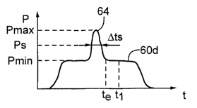
power profile 60c with a significant overshoot or "spike" 62 appearing at the
beginning of the laser pulse. The peak power of the overshoot is Pmax, and the
average power of the laser pulse is Pmin. The amplitude of the overshoot is
defined
as Pmax - Pmin. The width of the overshoot or "spike," Ots, is defined as the
full
duration time at the middle power point, Ps, between Pmax and Pmin. The peak
power of the overshoot or the "spike," Pmax, is preferably about 10% to about
50%
over the average power of the laser pulse, Pmin. The width of the overshoot or
"spike", its, is preferably 10% to 50% of the duration of the laser pulse. The
rise
time of the spike is typically shorter than about 5 ns, and preferably shorter
than
about.2 ns. Fig. 3D shows another embodiment of the invention that employs a
power profile 60d with an overshoot or "spike" 64 appearing not at the
beginning of
but during the laser pulse. The overshoot or "spike" ends at time, te, which
is before
the time, t~, when the link material is totally removed by the laser energy.
For
purposes of convenience, the term "spike" is used throughout the remainder of
the
application to indicate a significant, transient increase in laser power,
irrespective of
when it occurs during the laser pulse.
[0039] Fig. 3E shows the conditions of the passivation layers after link 22
has
been removed by a laser with laser pulse power profile 60c or 60d. Passivation
layer
44 overlaying a top surface 70 of link 22 has an opening 72 that extends
beyond
width 28 of link 22 by a relatively small amount, e.g., about the thickness of
overlying
passivation layer 44. Intermediate passivation layer 48 material positioned
adjacent
side surfaces 52 of link 22, passivation layer 46 underlying a bottom surface
74 of
link 22, and substrate 42 are not appreciably damaged. Fig. 3E shows an
irregularly
8
CA 02535623 2006-02-13
WO 2005/016586 PCT/US2004/026977
curved line 76 passing through portions of passivation layers 44, 46, and 48
surrounding the open area previously occupied by removed link 22. Curved line
76
represents typical damage to the passivation structure, specifically damage
that
extends by a certain amount, e.g., about 0.5 micron, from the region
previously
occupied by the link or becomes quite visible under a microscope. Typical
damage
also includes cracks in the passivation structure, which are not shown in the
drawing
figures.
(0040] Figs. 4-6 show several preferred embodiments implementing laser pulse
power profile tailoring and their associated specially tailored laser pulse
power
profiles employed to sever links 22 in accordance with the present invention.
Depending on the wavelength of laser output and the characteristics of the
link
material, tailoring of the power profile of a laser pulse provides it with
sufficient peak
power and energy of the pulse and proper duration to sever the link. After
completion of link material removal, the power profile and remaining duration
of the
laser pulse are tailored to impose no risk of damage to the substrate and
neighboring
structure of the link undergoing the process, even if the laser wavelength
used is
shorter than 1.3 Nm, in the visible range, or in the UV range.
[0041] Preferably, each laser pulse 37 severs a single link 22. (Unless
otherwise
indicated, the references to laser pulse 37 and focused spot size 40 (both
shown in
Fig. 2A) in connection with the descriptions of preferred embodiments relate
to
emission of laser pulses and not to prior art power profiles associated with
them). At
a preferred wavelength from about 250 nm to about 2000 nm, preferred ablation
parameters of focused spot size 40 of laser pulses 37 include laser energies
of each
laser pulse of between about 0.005 NJ and about 10 NJ, the duration of each
laser
pulse 37 is preferably shorter than about 40 ns and longer than about 1 ns,
laser
pulse repetition rate is greater than 1 Hz, more preferably within 10 KHz and
60 KHz
or higher and may be a function of the speed of the positioning system 380.
(Fig. 7)
and the distance between adjacent links 22 to be processed. The focused laser
spot
diameter is within the range of between about 0.5 Nm and about 3 Nm and
preferably
is about 40% to about 100% larger than the width of link 22, depending on link
width
28, link pitch size 32, link material, and other link structure and process
considerations.
9
CA 02535623 2006-02-13
WO 2005/016586 PCT/US2004/026977
[0042] With reference to Figs. 3C and 3D, the laser pulse power profiles 60c
and
60d, respectively, can be specially tailored to have a significant leading
edge
overshoot 62 (Fig. 3C) at the beginning of the laser pulse or have one or two
mid-
pulse spikes 64 (one spike shown in Fig. 3D) sometime within the duration of
the
laser pulse, before the link material is totally removed. Preferred timing of
the power
spike is within an interval measured from the rising edge of the laser pulse
power
profile to 70% of the duration of the laser pulse power profile. Fig. 3D shows
laser
pulse power profile 60d in which the power level is relatively flat before and
after
pulse spike 64. The laser pulse power profile can have a changing power level
before and after pulse spike 64. Tailoring the laser pulse power profile in
this
manner provides from leading edge overshoot or mid-pulse spikes sufficient
laser
peak power and energy to facilitate the satisfactory removal of the link
material and,
upon removal of most of the link material, much lower laser pulse power to
remove
remaining link material and ensure reduced risk of damage to the silicon
substrate
and to the structure neighboring the link. As a result, such special tailoring
of the
laser power profile delivers much better processing results and a wider
process
window and reduces risk of damage to the silicon substrate and to the
structure
neighboring the link.
[0043] With reference to Fig. 4A, in a first embodiment, special tailoring of
the
laser pulse power profile is accomplished by combining two laser pulses from
two
separate laser rails 110 and 112. Laser rail 110 generates a shorter laser
pulse 114,
shown in~Fig. 4B, and laser rail 112 generates a longer laser pulse 118, shown
in
Fig. 4C. The synchronization of or delay time (td) between laser pulses 114
and 118
is controlled by synchronizing electronics 120. Laser pulses 114 and 118 are
combined by a beam combiner 130 after laser pulse 118 reflects off a mirror
131 and
propagates through a waveplate 132 for polarization control purposes. Fig. 4D
shows a combined laser pulse 134 that has a final power profile with a
significant
power spike 136 preferred for link processing. The total laser pulse width of
combined laser pulse 134 can be either the sum of the widths of laser pulses
114
and 118 or the width of laser pulse 118, depending on the delay time between
laser
pulses 114 and 118. The widths of laser pulses 114 and 118 can be optimized
for
the link processing based on the link structure. Combined laser pulse 134 can
be
configured such that an additional power spike occurs at, for example, ta,
after power
CA 02535623 2006-02-13
WO 2005/016586 PCT/US2004/026977
spike 136. The additional power spike would preferably have a power value that
is
more than 5% of the average power of the combined laser pulse 134.
[0044] The timing of the spike 136 at time tp can also be readily program
controlled by synchronizing electronics 120 for the best link processing
quality and
yield. Skilled persons in the art will appreciate that, because they propagate
from
different laser rails and travel along different beam paths before combination
by
beam combiner 130, laser pulses 114 and 118 can be manipulated to have
different
beam spot sizes to further facilitate the link processing.
(0045] Typically, after beam combiner 130 combines laser pulses 114 and 118,
their polarization states are different from their original polarization
states. For
instance, the energy of laser pulse 114 can be vertically polarized while the
energy
of laser pulse 118 can be horizontally polarized. With the combined laser
energy
polarization states, the orientation of the target link or wafer mounted on a
system
worktable can be changed accordingly for the best processing quality and
yield. An
optional waveplate 140 can be inserted along the propagation path of combined
laser pulse 134 so that all of the laser energy is circularly polarized, if
such a
configuration delivers a better processing quality and yield for a particular
link
structure.
[0046] With reference to Fig. 5A, in a second embodiment, an E-O gating device
150 shapes the power profile of laser pulses propagating from a diode-pumped,
Q-switched solid state laser 152. Laser 152 delivers multiple laser pulses 160
(one
shown in Fig. 5B), each with a relatively long laser pulse width at full
width, half
maximum (FWHM). The FWHM pulse width can be, for example, about 30 ns to
50 ns. Laser pulses 160 propagate through E-O gating device 150. The output
laser
pulse power profile depends on the width and shape of a drive voltage pulse
162
delivered from drive electronics 164 and the delay time between laser pulse
160 and
the drive voltage pulse 162 applied to E-O device 150. The output laser pulse
can
have an upwardly, substantially linearly inclined (increasing) power profile,
as shown
for laser pulse 166c in Fig. 5C or a downwardly, substantially linearly
inclined
(decreasing) power profile with a higher peak at the very beginning of the
laser
pulse, as shown for laser pulse 166d in Fig. 5D. The total power decline after
the
peak is more than about 10% of the average power of the laser output pulse.
Persons skilled in the art will appreciate that the width and shape of the
voltage
11
CA 02535623 2006-02-13
WO 2005/016586 PCT/US2004/026977
pulse itself applied to E-O device 150 can be tailored to provide greater
flexibility in
tailoring the width and power profile of laser pulse 166.
[0047] With reference to Fig. 6A, in a third embodiment, a laser 200 is
composed
of an injection laser 202 followed by an amplifier 204. Injection laser 202
can be a
diode laser having a fast response time and delivering laser output at a laser
wavelength that matches the gain spectrum of amplifier 204. Fig. 6B shows a
specially tailored drive current pulse 206 delivered from driving electronics
208, and
Fig. 6C shows that an injection laser output pulse 210 propagating from
injection
laser 202 replicates the profile of drive current pulse 206 as a result of the
fast
response capability of injection laser 202. Injection laser output pulse 210
is
delivered to laser power amplifier 204, which is operating in an unsaturated
state to
amplify injection laser output pulse 210 and deliver an output pulse 212
without
introducing significant distortion of the tailored laser pulse power profile,
as shown in
Fig. 6D. Output pulse 212 is relatively flat after the occurrence of the power
spike
and before the falling edge of the laser pulse temporal power profile. Persons
skilled
in the art will appreciate that the profile of drive current pulse 206 can be
readily
programmed to any preferred profile in accordance with this invention. Persons
skilled in the art will also appreciate that the gain requirement of amplifier
204
depends on the laser pulse power available from injection laser 202 and the
power of
the laser output pulse 212 required for this invention.
[0048] Figs. 6E and 6F show, respectively, a drive current profile 214 and its
replicated laser pulse power profile 216 produced in accordance with a
different
implementation of the third embodiment of Fig. 6A. Drive current profile 214
is
composed of a pulse with three time-displaced current spikes 218, 220, and 222
of
decreasing values over time at t~, t2, t3, respectively. Current spikes 218,
220, and
222 produce for laser pulse power profile 216 corresponding power spikes 224,
226,
and 228. Power spike 224 represents an overshoot occurring at the rising edge
of
laser pulse power profile 216, and power spikes 226 and 228 represent
subsequent
power spikes occurring during the pulse but before the target link material is
completely removed. Power spikes 224, 226, and 228 together form a composite
power spike in the form of an oscillating wave with a power variation of over
about
10% of the average power of the laser output pulse. The oscillating wave can
last
from about one-half cycle to three cycles of duration within the duration of
the laser
12
CA 02535623 2006-02-13
WO 2005/016586 PCT/US2004/026977
pulse power profile. The period of the oscillation cycle is preferably between
about
1 ns and about 15 ns.
[0049] One preferred embodiment of amplifier 204 is a fiber laser amplifier.
The
length of the fiber, type of lasing dopant, doping level, and pumping level
can be
tailored to realize the required amplification gain. An exemplary laser 200
can be a
modification of a fiber laser manufactured by IMRA, America, Inc., Fremont, CA
and
IPG Photonics Corp., Oxford, MA. Both IMRA and IPG manufacture laser devices
that include a fast laser diode operating as the injection laser followed by a
fiber
power amplifier. The laser wavelength is tunable in the 1.06 Nm to 1.1 pm
range.
The laser pulse shape is substantially square shaped with a pulse width
programmable from 5 ns to 20 ns, laser energy of 0.1 NJ to 10 pJ, and laser
pulse
repetition rate of about 20 KHz. With the tailoring of the drive current
supply to the
fast diode laser, the laser pulse power profile can be tailored as described
for the
present invention. Another exemplary fiber laser manufactured by INO, Quebec,
Canada implements a special technique to get the injection laser pulse from
the fiber
itself and then use the fiber to amplify the injection pulse. Its currently
available
version works at a laser wavelength of 1.57 pm, and its pulse profile is very
similar to
that shown in Fig. 6F. According to INO, it is not difficult to make a similar
laser
working at wavelength of 1.06 Nm to 1.1 Nm with a different tailored laser
pulse
profile.
[0050] With reference to Figs. 4, 5, and 6, the preferred laser wavelengths
are in
the spectral range from about 150 nm to about 2000 nm, and include, but are
not
limited to, 1.54, 1.3, 1.1 - 1.06, 1.05, 1.047, 1.03 - 0.75 Nm or their
second, third,
fourth, or fifth harmonics from Nd:YAG, Nd:YLF, Nd:YV04, Yb:YAG, Ti:Sapphire,
and
fiber lasers with different base materials and doping. Skilled persons will
appreciate
that lasers emitting output pulses at other suitable wavelengths are
commercially
available and could be employed. Skilled persons will also appreciate that any
of the
second, third, or fourth harmonics of Nd:YAG (532 nm, 355 nm, 266 nm); Nd:YLF
(524 nm, 349 nm, 262 nm); or the second harmonic of Ti:Sapphire (375 nm -
425 nm) can be employed to preferably process certain types of links 22 and/or
passivation layers 44 using appropriate well-known harmonic conversion
techniques.
Harmonic conversion processes are described in V.G. Dmitriev, et al., Handbook
of
NonlinearOpfical Crystals, 138-141, Springer-Verlag, New York, 1991 ISBN 3~540-
53547-0.
13
CA 02535623 2006-02-13
WO 2005/016586 PCT/US2004/026977
[0051] With reference to Fig. 7, laser system 300 is modeled herein only by
way
of example to a 1.064 Nm Nd:YAG laser 302. The Nd:YAG or other solid-state
laser
302 is preferably pumped by a laser diode 304, the emission 306 of which is
focused
by fens components 308 into a laser resonator 310. Laser resonator 310
preferably
includes a lasant 312, a Q switch 314, and an optional polarizer 315
positioned
between resonator mirrors 316 and 318 along an optic axis 320. An aperture 330
may also be positioned between lasant 312 and mirror 318. A laser output pulse
334
propagates along optic axis 320 through mirror 318, which functions as a
partly
reflective output coupler. In one embodiment of the invention, laser pulse 334
propagating from laser 302 is incident on an optional optical component or
device 336, such as a waveplate, a polarizer, or an isolator, and then
undergoes the
special intensity profile tailoring with an E-O gating device 340, controlled
by a
subcontroller 342.
[0052] Regardless of wavelength or laser type, laser output 350 of gating
device
340 can be manipulated by a variety of conventional optical components 352 and
354 that are positioned along a beam path 356. Components 352 and 354 may
include a beam expander or other laser optical components to collimate laser
output
350 to produce a beam with useful propagation characteristics. One or more
beam
reflecting mirrors 358, 360, 362, and 364 that are highly reflective at the
laser
wavelength desired, but highly transmissive at the unused wavelengths, are
optionally employed so that only the desired laser wavelength will reach link
structure 36. A focusing lens 366 preferably employs a single component or
multicomponent lens system that focuses a collimated pulsed laser system
output
368 to produce a focused spot size 40 that is greater than and thereby
encompasses
link width and is preferably less than 2 Nm in diameter or smaller, depending
on the
link width 28 and the laser wavelength.
[0053] A preferred beam positioning system 380 composed of optical
components 358, 360, 362, and 364 is described in detail in U.S. Patent
No. 4,532,402 of Overbeck for Method and Apparatus for Positioning a Focused
Beam on an Integrated Circuit. Beam positioning system 380 preferably employs
a
laser controller 382 that controls at least two platforms or stages (stacked
or split-
axis) and coordinates with beam reflecting mirrors 358, 360, 362, and 364 to
target
and focus laser system output 368 to a selected conductive link 22 on IC
device or
work piece 12. Beam positioning system 380 permits quick movement between
links
14
CA 02535623 2006-02-13
WO 2005/016586 PCT/US2004/026977
22 on work piece 12 to effect unique link-severing operations on-the-fly,
based on
provided test or design data.
[0054] The position data preferably direct the focused laser spot 38 over work
piece 12 to target link structure 36 with one laser pulse of laser system
output 368 to
remove link 22. Laser system 300 preferably severs on-the-fly with a single
laser
pulse 37 each of links 22 to be severed. Laser system 300 accomplishes this
process without stopping beam positioning system 380 over any link 22, so that
high
throughput is realized. Persons skilled in the art will appreciate that such
laser
systems 300 equipped with conventional diode pumped, Q-switched solid-state
lasers are commercially available and well known to skilled practitioners.
[0055] Laser controller 382 is provided with instructions concerning the
proper
process of the selected links. Laser controller 382 may be influenced by
timing data
that synchronizes the firing of laser system 300 to the motion of the
platforms such
as described in U.S. Patent No. 5,453,594 of Konecny for Radiation Beam
Position
and Emission Coordination System. Alternatively, in one embodiment of the
present
invention, skilled persons will appreciate that laser controller 382 is used
for
extracavity modulation of laser energy by an E-O device 340 and instructs
subcontrollers 342 and 386 that control Q-switch 314, E-O device 340, and
pumping
diode 304.
[0056] With reference to Figs. 2A-2C, in view of the foregoing, link
processing
with laser pulse 37 of a specially tailored power profile offers a wider
processing
window and a superior quality of severed links than does link processing with
a laser
pulse of conventional power profile. The overshoot at the beginning of the
laser
pulse and/or spike properly timed within the duration time of the laser pulse
ensures
that an adequate amount of laser energy is coupled into the link structure
within a
proper time period before all the link material of the selected link is
removed. This is
accomplished with adequate processing margin for the inevitable variations of
the
link structure and the laser parameters themselves. After most of the link
material is
removed by the laser energy, the laser pulse power is specially tailored to
have
much lower value compared to the peak power of the laser pulse, or the power
of the
overshoot and spike. Thus, this specially tailored laser pulse power profile
ensures
less risk of damage to the neighboring structures and silicon substrate 42. In
addition to conventional link blowing IR laser wavelengths, laser wavelengths
shorter
than the IR wavelengths can also be used for the process with the added
advantage
CA 02535623 2006-02-13
WO 2005/016586 PCT/US2004/026977
of smaller laser beam spot size, even though the absorption of a silicon wafer
at the
shorter laser wavelengths is higher than that at the conventional IR
wavelengths.
Thus, the processing of narrower and denser links is facilitated. This better
link
removal resolution permits links 22 to be positioned closer together, thereby
increasing circuit density. Although link structures 36 can have conventional
sizes,
the link width 28 can, for example, be less than or equal to about 0.5 pm.
[0057] Similarly, the versatility of better tailoring the laser pulse power
profile
offers better flexibility in accommodating different passivation
characteristics.
Passivation layers 44 above or passivation layers 46 below links 22 can be
made
with material other than the traditional materials or can be modified, if
desired to be
other than a typical height. This is so because the laser pulse can be
tailored,
thereby reducing the risk of damage to the underlying or neighboring
passivation
structure. In addition, wavelengths that are much shorter than about 1.06 Nm
can be
employed to produce critical spot size diameters 40 of less than about 2 arm
center-
to-center pitch 32 between links 22. Links processed with laser pulses from
shorter
wavelength lasers can, therefore, have a substantially smaller center-to-
center pitch
32 than that possible for links blown by a conventional IR laser beam-severing
pulse.
Link 22 can, for example, be within a distance of 2.0 Nm or less from other
links 22 or
adjacent circuit structures 34.
[0058] Overlying passivation layer 44 may include any conventional passivation
materials such as silicon dioxide (Si02) and silicon nitride (Si3N4).
Underlying
passivation layer 46 may include the same passivation material as or different
passivation materials) from overlying passivation layer 44. In particular,
underlying
passivation layer 46 in target structures 36 may comprise fragile materials,
including
but not limited to, materials formed from low K materials, low K dielectric
materials,
low K oxide-based dielectric materials, orthosilicate glasses (OSGs),
fluorosilicate
glasses, organosilicate glasses, tetraethylorthosilicate (TEOS)-based oxides,
methyltriethoxyorthosilicate (MTEOS), propylene glycol monomethyl ether
acetate
(PGMEA), silicate esters, hydrogen silsesquioxane (HSQ), methyl silsesquioxane
(MSQ), polyarylene ethers, benzocyclobutene (BCB), SiCOH, or SiCOH-derived
film
(such as "Black Diamond" sold by Applied Materials, Inc.), or spin on-based
low K
dielectric polymer (such as "SILK" sold by Dow Chemical Company). Underlying
passivation layers 46 made from some of these materials are more prone to
crack
when their targeted links 22 are blown or ablated by conventional single laser-
pulse
16
CA 02535623 2006-02-13
WO 2005/016586 PCT/US2004/026977
link-removal operations. Skilled persons will appreciate that Si02, SiON,
Si3N4, low
K materials, low K dielectric materials, low K oxide-based dielectric
materials, OSGs,
fluorosilicate glasses, organosilicate glasses, HSQ, MSQ, BCB, SiLKT"", and
Black
DiamondTM are actual layer materials, and TEOS, MTEOS, and polyarylene ethers
are semiconductor condensate precursor materials.
[0059] It will be obvious to those having skill in the art that many changes
may be
made to the details of the above-described embodiments without departing from
the
underlying principles of this invention. The scope of the present invention
should,
therefore, be determined only by the following claims.
17