Note: Descriptions are shown in the official language in which they were submitted.
CA 02535717 2006-02-13
WO 2005/027607 PCT/US2004/027566
1
LASER MONITORING AND CONTROL IN A TRANSMITTER OPTICAL
SUBASSEMBLY HAVING A CERAMIC FEEDTHROUGH HEADER
ASSEMBLY
The Field of the Invention
The present invention generally relates to optoelectric systems and devices.
More specifically, embodiments of the present invention relate to a transistor
header
assembly for use in an optical transceiver module, wherein the header assembly
includes various features directed to monitoring and adjusting a laser device
of the
transceiver for optimum performance.
The Related Technology
Fiber-optic components and opto-electronics have become important
components in modern networking circuits. The use of fiber-optic circuits
allows for
efficient, accurate and quick transmission of data between various components
in a
network system.
As with the design of most any system, there are engineering tradeoffs that
often have to be made when implementing fiber optic systems. For example, the
size
and modularity of components must often be balanced against the need for
additional
space to accommodate heat dissipation and circuit monitoring components. While
it
is desirable to minimize a component's size, some configurations have
previously
limited this minimization due to their inherent characteristics. For example,
previously many lasers used in fiber-optic systems that have the
characteristics
needed for long-distance transmission and/or dense wavelength division
multiplexing
(DWDM) generated amounts of heat that could not be dissipated by some smaller
package sizes. Further, smaller package sizes have a limited amount of space
available for mounting and connecting additional components such as
thermistors,
monitor photodiodes, thermoelectric coolers, or impedance matching circuits.
Regarding smaller package sizes, it is desirable in fiber optic systems to use
modular components so that a system can be created in a compact area and with
as
little expensive customization as possible. For example, many fiber optic
systems are
able to use modular transceiver modules. The modular transceiver modules
include
an input receiver optical subassembly (ROSA) and an output transmitter optical
CA 02535717 2006-02-13
WO 2005/027607 PCT/US2004/027566
2
subassembly (TOSA). The ROSA comprises a photodiode for detecting optical
signals and sensing circuitry for converting the optical signals to digital
signals
compatible with other network components. The TOSA comprises a laser for
transmitting optical signals and control circuitry for modulating the laser
according to
an input digital data signal. The TOSA has an optical lens for focusing the
light
signals from the laser of the TOSA to an optical fiber. Additionally, the
transceiver
module includes pluggable receptacles for optically connecting the TOSA and
the
ROSA with other components within a fiber optic network.
The transceiver module often includes an electronic connector for connection
to electrical components of the computer or communication device with which
the
transceiver module operates (a "host system"). The design of the transceiver,
as well
as other components within the fiber optic system, is standards-based, such
that
components can be connected without significant customization.
One particular pluggable standard that is currently being developed is the 10-
Gigabit Small Form-factor Pluggable (XFP) standard. This standard defines
various
characteristics such as size, power consumption, connector configuration, etc.
With
regards to power consumption, the XFP standard references three power
consumption
levels of 1.5 W, 2.5 W and 3.5 W. When designing devices to operate within the
XFP
standard, attention must be given to what components are selected and how they
are
configured so as to not exceed the rated power consumption. These devices are
constrained by principles of semiconductor physics to work preferentially in a
certain
temperature range. The module power dissipation and the package size and
materials
uniquely determine the module operating temperature for given ambient
conditions,
such as ambient temperature, airflow, etc. The resulting module operating
temperature determines the types of optical and electronic components that can
be
successfully operated within the package. One such package is known as a
transistor-
outline header, otherwise known as a TO can or TO.
Transistor-outline headers are widely used in the field of opto-electronics,
and
may be employed in a variety of applications. As an example, transistor
headers are
sometimes used to protect sensitive electrical devices, and to electrically
connect such
devices to components such as printed circuit boards ("PCB").
CA 02535717 2006-02-13
WO 2005/027607 PCT/US2004/027566
3
With respect to their construction, transistor headers often consist of a
cylindrical metallic base with a number of conductive leads extending
completely
through, and generally perpendicular to, the base. With regard to the metallic
base,
the size of the base is often sized to fit within a specific TO standard size
and lead
configuration, examples of which include a TO-5 or TO-46. The leads are
hermetically sealed in the base to provide mechanical and environmental
protection
for the components contained in the TO package, and to electrically isolate
the
conductive leads from the metallic material of the base. Typically, one of the
conductive leads is a ground lead that may be electrically connected directly
to the
base.
Various types of devices are mounted on one side of the base of the header
and connected to the leads. Generally, a cap is used to enclose the side of
the base
where such devices are mounted, so as to form a chamber that helps prevent
contamination or damage to those device(s). The specific characteristics of
the cap
and header generally relate to the application and the particular device being
mounted
on the base of the header. By way of example, in applications where an optical
device
is required to be mounted on the header, the cap is at least partially
transparent so to
allow an optical signal generated by the optical device to be transmitted from
the TO
package. These optical TO packages are also known as window cans.
Although transistor headers have proven useful, typical configurations
nevertheless pose a variety of unresolved problems. Some of such problems
relate
specifically to the physical configuration and disposition of the conductive
leads in
the header base. As an example, various factors combine to compromise the
ability to
precisely control the electrical impedance of the glass/metal feedthrough,
that is, the
physical bond between the conductive lead and the header base material. One
such
factor is that there are a relatively limited number of available choices with
respect to
the diameter of the conductive leads that are to be employed. Further, the
range of
dielectric values of the sealing glass typically employed in these
configurations is
relatively small. And, with respect to the disposition of the conductive
leads, it has
proven relatively difficult in some instances to control the position of the
lead with
respect to the through hole in the header base.
CA 02535717 2006-02-13
WO 2005/027607 PCT/US2004/027566
4
Yet other problems in the field concern those complex electrical and
electronic
devices that require many isolated electrical connections to function
properly.
Typically, attributes such as the size and shape of such devices and their
subcomponents are sharply constrained by various form factors, other
dimensional
requirements, and space limitations within the device. Consistent with such
form
factors, dimensional requirements, and space limitations, the diameter of a
typical
header is relatively small and, correspondingly, the number of leads that can
be
disposed in the base of the header, sometimes referred to as the input/output
("I/O")
density, is relatively small as well.
Thus, while the diameter of the header base, and thus the I/O density, may be
increased to the extent necessary to ensure conformance with the electrical
connection
requirements of the associated device, the increase in base diameter is
sharply limited,
if not foreclosed completely, by the form factors, dimensional requirements,
and
space limitations associated with the device wherein the transistor header is
to be
employed.
In connection with the foregoing, another limiting aspect of many transistor
headers relates to the relatively limited physical space available on the
header. In
particular, the relatively small amount of space on the base of the header
imposes a
practical limit on the number of components that may be mounted thereon. To
overcome that limit, some or all of any additional components desired to be
used must
instead be mounted on the printed circuit board, some distance away from the
laser or
other device contained within the transistor header. Such arrangements are not
without their shortcomings however, as the performance of active devices in
the
transistor header, such as lasers and integrated circuits, depends to some
extent on the
physical proximity of related electrical and electronic components. By
minimizing
the distance between the lasers and integrated circuits to the additional
components
required for impedance matching, the inherent transmission line between such
components is minimized. As such, placing the components in close physical
proximity reduces reflective transmission line losses.
In addition to the above, further challenges are faced when certain functions
are desired to be added to the transistor header. In particular, it is
beneficial to
monitor and/or modify the character of the optical signal that is produced and
emitted
CA 02535717 2006-02-13
WO 2005/027607 PCT/US2004/027566
by the laser device of the TOSA. For instance, the optical signal that is
output by the
laser device can change in power and/or wavelength over time as the laser
heats up
within the TOSA during operation of the optical transceiver module. If these
laser
parameters are actively monitored during transceiver operation, adjustment can
be
5 made to the laser device to ensure its proper operation.
Monitoring of laser device parameters such as power and output wavelength is
typically accomplished using one or more monitor photodiodes ("MPD"). In the
case
of laser power monitoring, a single MPD is often used, while wavelength
monitoring
typically requires two MPDS working in concert. In either case, it is
desirable to
locate the one or more MPDs within the transistor header assembly in close
proximity
to the laser device so that laser light produced by the laser device can be
received by
the MPDs. However, as has already been explained, the location of
optoelectronic
devices within the transistor header assembly requires additional electrical
interconnects to be passed through the header assembly, which may not be
possible in
known header assembly designs that must comply with prescribed dimensional
form
factors. Thus, the use of one or more MPDs within a transistor header assembly
may
be restricted or foreclosed completely.
In light of the above discussion, a need exists for a transistor header design
for
use within an optical transceiver module that overcomes the above challenges.
In
particular, a transistor header is needed that enables a relatively greater
number of
interconnects to be established between the header interior and devices
located
outside of the header. Such a solution should also enable the utilization of
monitoring
devices, such as one or more monitor photodiodes, within the transistor header
assembly to optimize the operation of optoelectronic components, such as a
laser
device, located therein.
BRIEF SUMMARY OF THE INVENTION
The present invention has been developed in response to the above and other
needs in the art. Briefly summarized, embodiments of the present invention are
directed to a transistor header assembly that includes various features
directed to
enhancing the reliability and performance of various optoelectronic devices,
such as a
laser, that are located within the header assembly. In particular, presently
preferred
embodiments include a header assembly that enables the incorporation therein
of one
CA 02535717 2006-02-13
WO 2005/027607 PCT/US2004/027566
6
or more monitoring devices, such as a monitor photodiode, in order to optimize
operation of the laser. This is accomplished while concurrently preserving the
size of
the header assembly within predefined form factor restrictions.
In one illustrative embodiment of the invention, a transistor header is
disclosed
having a platform extending through a base of the header. The platform
includes
multiple stacked layers, wherein each layer defines a plurality of specified
conductive
pathways that extend through the header base to interconnect optoelectronic
devices
disposed on a portion of the platform inside the header with other components
disposed outside of the header. The multi-layer design of the platform allows
not
only for a relative increase in the number of interconnects available for use
within the
header, but also for the electrical isolation of the conductive pathways from
other
portions of the header assembly to enable their passage from the exterior
portion to
the interior portion thereof.
The multi-layer platform further enables specialized components to be
positioned within the header assembly to enhance its operation. Such
components
include, for example, EML laser device configurations and thermo-electric
coolers.
Particularly, in one presently preferred embodiment the multi-layer platform
provides
for the placement of one or more monitor photodiodes within the header
assembly to
monitor the operation of the laser device. Parameters of the laser that can be
monitored and/or controlled by the monitor photodiode(s) include the power and
wavelength of the optical signal that is emitted by the laser.
To monitor laser power, a single monitor photodiode ("MPD") is located
within the header assembly on a submount that is operably attached to the
multi-layer
platform. The MPD is positioned in close proximity to a laser, such as a
distributed
feedback laser, that is also located on the submount. Back emission of light
from the
laser is received by the MPD, which then determines the power of the laser
output.
Adjustments to the laser can then be made based on the measurement of the MPD
in
order to optimize laser operation.
To monitor laser wavelength, two MPDs (which together operate as a
wavelength locker) are located on the submount in close proximity to the
laser. Back
emission of light from the laser is received by both MPDs, one of which
includes a
wavelength-dependent filter. Each MPD produces a measurement signal according
to
CA 02535717 2006-02-13
WO 2005/027607 PCT/US2004/027566
7
the laser light received thereby, with the strength of the measurement signal
of the
filtered MPD varying according to the wavelength of the light received from
the laser.
A ratio comparison of the two measurement signals produced by the respective
MPDs
yields the wavelength of the optical signal being produced by the laser. In
this way,
any needed modification of the optical signal output of the laser can be
determined
and performed to optimize the quality of the signal.
In either of the two cases above (i.e., single or double MPDs), multiple
electrical interconnects passing through the header assembly are needed in
order to
provide the necessary electrical connectivity of the MPDs. In accordance with
the
present invention, these interconnects are readily provided by virtue of the
multi-layer
platform design as disclosed herein, which design provides multiple
interconnects
between exterior and interior portions of the header assembly without
compromising
the size restrictions of the header assembly. This ultimately results in
enhanced
performance not only for the header assembly and optoelectronic components
disposed therein, but for the optical subassembly containing the header
assembly, and
the optical transceiver as a whole. Alternatively, the header assembly can be
employed in other electronic package configurations, such as transmitters,
receivers,
transponders, etc.
These and other features of the present invention will become more fully
apparent from the following description and appended claims, or may be learned
by
the practice of the invention as set forth hereinafter.
BRIEF DESCRIPTION OF THE DRAWINGS
To further clarify the above and other advantages and features of the present
invention, a more particular description of the invention will be rendered by
reference
to specific embodiments thereof that are illustrated in the appended drawings.
It is
appreciated that these drawings depict only typical embodiments of the
invention and
are therefore not to be considered limiting of its scope. The invention will
be
described and explained with additional specificity and detail through the use
of the
accompanying drawings in which:
Figure IA is a perspective view illustrating various aspects of the device
side
of an exemplary embodiment of a header assembly;
CA 02535717 2006-02-13
WO 2005/027607 PCT/US2004/027566
8
Figure 1B is a perspective view illustrating various aspects of the connector
side of an exemplary embodiment of a header assembly;
Figure 2A is a perspective view illustrating various aspects of the device
side
of an alternative embodiment of a header assembly;
Figure 2B is a perspective view illustrating various aspects of the connector
side of an alternative embodiment of a header assembly;
Figure 3A is a perspective view illustrating various aspects of the device
side
of another alternative embodiment of a header assembly;
Figure 3B is a perspective view illustrating various aspects of the connector
side of another alternative embodiment of a header assembly;
Figure 4 is a perspective view of a transmitter optical subassembly having a
header assembly configured in accordance with another embodiment of the
present
invention;
Figure 5A is a perspective view of the header assembly comprising part of the
transmitter optical subassembly shown in Figure 4;
Figure 5B is a side view of the header assembly of Figure 5A;
Figure 6A is a perspective view of the header assembly of Figure 5A with the
circular base removed;
Figure 6B is a top view of the header assembly of Figure 6A;
Figure 7 is a top view of one layer of the multi-layer platform of the header
assembly of Figure 5A;
Figure 8 is a top view of another layer of the multi-layer platform of the
header assembly of Figure 5A;
Figure 9 is a perspective view of a header assembly and corresponding
submount comprising part of a transmitter optical subassembly according to one
embodiment of the present invention;
Figure 10 is a side view of the header assembly and submount of Figure 9;
Figure 11 is a close-up view of a portion of the header assembly of Figure 10,
showing various optoelectronic components located on the submount according to
one
embodiment of the present invention;
CA 02535717 2006-02-13
WO 2005/027607 PCT/US2004/027566
9
Figure 12 is a perspective view of a header assembly and corresponding
submount comprising part of a transmitter optical subassembly according to
another
embodiment of the present invention; and
Figure 13 is a close-up view of a portion of the submount of Figure 12,
showing various features of certain optoelectronic components.
DETAILED DESCRIPTION OF THE PREFERRED EMBODIMENTS
Reference will now be made to figures wherein like structures will be
provided with like reference designations. It is understood that the drawings
are
diagrammatic and schematic representations of presently preferred embodiments
of
the invention, and are not limiting of the present invention nor are they
necessarily
drawn to scale.
Figures 1-13 depict various features of embodiments of the present invention,
which is generally directed to an improved header assembly that permits
enhanced
functionality of components disposed therein. In particular, various
embodiments of
the present invention disclose a multi-layer feedthrough structure that is
integrated
with the header assembly for use in small form factor optical transceiver
modules.
The multi-layer configuration of the feedthrough enables a significant
expansion of
both the number and types of electro-optic components that can be positioned
within
the header assembly. Indeed, in presently preferred embodiments, one or more
monitor photodiodes are located within the header assembly to monitor various
parameters of a laser device. Both the monitor photodiode(s) and the laser
device are
located on a component submount, which is in turn electrically connected to
the
multi-layer platform. Because of the relatively high number of electrical
interconnects provided by the multi-layer platform, the inclusion of one or
more
photodiodes within the header assembly to operate in conjunction with the
laser
device is facilitated. This in turn results in enhanced flexibility in
transceiver design
as well as in improved control thereof.
In particular, the monitor photodiodes can be mounted such that light emitted
from a back facet of the laser is detected. Using light emitted from the back
facet, the
monitor photodiode can monitor the power of the laser.
Similarly, a wavelength locker (comprising, in one embodiment, multiple
monitor photodiodes) can use light emitted from the back facet to monitor the
CA 02535717 2006-02-13
WO 2005/027607 PCT/US2004/027566
wavelength and/or power of the laser. The multi-layer configuration of the
feedthrough provides sufficient electrical interconnects to permit monitor
photodiodes
or other devices to be located near the laser.
In one embodiment, the header assembly of the present invention is configured
5 for use within optical transceiver modules adhering to the XFP standard. At
the time
of the filing of this patent application, the XFP standard is the XFP Adopted
Revision
3.1, promulgated by the 10 Gigabit Small Form Factor Pluggable (XFP) Multi
Source
Agreement (MSA) Group. This XFP Adopted Revision 3.1 document is incorporated
herein by reference. As used herein, the terms "XFP standard" and "XFP Multi
10 Source Agreement" refer to the Adopted Revision 3.1. These terms also refer
to any
subsequent drafts or final agreements to the extent that any such subsequent
drafts or
final agreements are compatible with Adopted Revision 3.1.
1. Header Assemblies
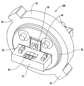
Reference is first made to Figures 1A and 1B together, which illustrate
perspective views of one presently preferred embodiment of a header assembly,
designated generally at 200. In the illustrated example, the header assembly
200
includes a substantially cylindrical metallic base 10. The base 10 includes
two
flanges 90 for releasably securing the header 200 to a receptacle (not shown)
on a
higher level opto-mechanical assembly. The base can be formed of Alloy 42,
which
is an iron nickel alloy, as well as cold-rolled steel, Vacon VCF-25 Alloy,
Kovar, or
other suitable material. The base 10 also includes a ceramic platform 70
extending
perpendicularly through the base as shown. The ceramic platform is
hermetically
sealed to the base to provide mechanical and environmental protection for the
components contained in the TO package. Ceramic materials may include, but are
not
limited to, alumina (A1203) or aluminum nitride (A1N).
The hermetic seal between the base 10 and the platform 70 is created by
electrically insulating glass-to-metal seals. Alternatively, the platform 70
may
incorporate two additional ceramic outer layers to electrically isolate the
outermost
conductors. In this second case, a metal braze or solder can be used to
hermetically
seal the platform 70 to the metal base. This solution overcomes the principal
shortcomings of glasses, namely their low strength, brittleness, and low
thermal
conductivity.
CA 02535717 2006-02-13
WO 2005/027607 PCT/US2004/027566
11
The platform 70 is structured to house multiple electrical components 50 and
100, and active devices 60 on either side of the base. In the illustrated
embodiment,
the active device 60 comprises a semiconductor laser, and the components 50
and 100
may include resistors, capacitors, and inductors that are used to balance the
driving
impedance of the laser with the component impedance. As discussed in more
detail
below, impedance matching circuits may also be created by etching electrical
traces
that have various capacitive, inductive or resistive properties, on platform
70. In
addition to matching, components may have peripheral functions such as
measuring
temperature, sensing laser optical power or wavelength, etc. As it is
important for a
semiconductor laser to be precisely positioned perpendicularly to the base 10,
platform 70 is, therefore, precisely positioned perpendicularly with respect
to the base
10.
Where active device 60 comprises a semiconductor laser, a small deviation in
the position of active device 60, in relation to base 10 can cause a large
deviation in
the direction of the emitted laser beam. Accurate perpendicularity between the
platform and the base can be achieved by incorporating a vertical pedestal
feature in
the base material, as shown on Figure 1A. The vertical pedestal houses the
photodiode
30 in the embodiment shown in Figure 1A. Such feature can be machined,
stamped,
or metal injection molded directly with the base thus providing a stable and
geometrically accurate surface for mating with the platform.
The platform 70 further includes multiple electrically isolated conductive
pathways 110 extending throughout the platform 70 and consequently through the
base 10. The conductive pathways 110 provide the electrical connections
necessary
between electrical devices or components located throughout the platform 70.
The
conductive pathways 110 form a connector on that side of the base that does
not
include the semiconductor laser 60, also referred to herein as the "connector
side" of
the base. Note in connection with the foregoing that the side of the base
where the
active device 60 is located may in some instances be referred to herein as the
"device
side" of the base.
The connector formed by the conductive pathways 110 is used to electrically
connect the header assembly 200 to a second electrical subassembly, such as a
printed
circuit board, either directly (for example, by solder connection) or
indirectly by an
CA 02535717 2006-02-13
WO 2005/027607 PCT/US2004/027566
12
intermediary device such as a flexible printed circuit. The semiconductor
laser 60 is
electrically connected to the electrical components 50 and 100 via the
conductive
pathways 110.
The platform 70 may also comprise multiple layers wherein each layer may
have a conductive layer with various conductive pathways 110. In this way
numerous
conductive pathways 110 may be constructed for use with various components
disposed on the platform 70. Generally, the layers are electrically isolated
from one
another, however various conductive pathways 110 on different layers may be
connected by a via such as is commonly known in printed circuit board arts.
Further, the conductive pathways 110 can be shaped and placed such that they
have controlled capacitive, inductive, or resistive effects to create
waveguides such as
a microstrip or stripline (cpw, etc.). For example, knowing certain
characteristics
about the materials used in making the conductive pathways 110 and the
materials of
the various layers of the platform 70, passive electrical devices can be
constructed by
appropriately configuring the conductive pathways 110. In this way, a
transmission
line with known characteristics can be created for use with active devices 60
attached
to the platform 70. As noted above, by matching the characteristics of the
transmission line connected to active devices 60 with the active devices' 60
load
impedance, electrical reflections that cause transmission errors and lower
power
output can be reduced or in many cases eliminated.
By constructing a transmission line that matches active device 60 impedance
on the platform 70 from the conductive traces 110, the need to add additional
discrete
matching components is eliminated often resulting in better overall circuit
performance. In fact, previously due to the lack of adequate matching
circuits,
applications involving transistor headers have been limited to 10 Gb/s. With
the
improvements of using a transmission line constructed on the platform 70,
applications up to 40 Gb/s or more can be implemented.
While the preceding description has discussed active devices 60 in terms of
lasers, it should be noted that the transmission lines may also be formed such
that a
matching circuit for other semiconductor devices is constructed. For example,
the
transmission lines may be used to connect directly to a laser, such as in the
case of
DFB lasers. Alternately, the transmission lines may be used to connect to an
EA
CA 02535717 2006-02-13
WO 2005/027607 PCT/US2004/027566
13
modulator, for example, such as in the case of EMLs that incorporate a DFB
laser and
an EA modulator. As discussed herein, the impedance values of the impedance
matching transmission lines depend on the load impedance of the active devices
attached to the platform 70.
External components, while still useful, are not ideal for impedance matching
because they often represent an additional load that must be driven by the
power
supply driving the electronic component, such as when resistors are used to
match the
active device 60 load impedance. Additionally, although the external
components
may be placed reasonably close to the active devices 60, there is always some
small
distance between the external components and the active devices 60 that acts
as an
unmatched transmission line.
The use of advanced ceramic materials, examples of which include aluminum
nitride and beryllia, allows the header assembly 200 to achieve substantially
lower
thermal resistances between the devices inside the package and the outside
world
where heat is ultimately transferred. As discussed in further detail below in
the
context of an alternative embodiment of the invention, a cooling device, such
as a
thermoelectric cooler ("TEC"), a heat pipe or a metal heat spreader, can be
mounted
directly on the platform, thereby providing for a very short thermal path
between the
temperature sensitive devices on the platform and a heat sink located outside
the
header assembly.
As is further shown in Figures 1A and 1B, the header assembly 200
additionally includes two conductive leads 40 extending through and out both
sides of
the base 10. The conductive leads 40 are hermetically sealed to the base 10 to
provide
mechanical and environmental protection for the components contained in the TO
package between the conductive leads 40 and the base 10. The hermetic seal
between
the conductive leads 40 and the base 10 is created, for example, by glass or
other
comparable hermetic insulating materials that are known in the art. The
conductive
leads 40 can also be used to electrically connect devices and/or components
located
on opposite sides of the base.
In the illustrated embodiment at least, the conductive leads 40 extend out
from
the side of the base 10 that does not contain the semiconductor laser 60, in a
manner
that allows for the electrical connection of the header assembly 200 with a
specific
CA 02535717 2006-02-13
WO 2005/027607 PCT/US2004/027566
14
header receptacle located on, for example, a printed circuit board. It is
important to
note that conductive pathways 110 and conductive leads 40 perform the same
function
and that the number of potential conductive pathways 110 is far greater than
the
potential number of conductive leads 40. Alternative embodiments can
incorporate
even more conductive pathways 110 than shown in the illustrated embodiment.
The platform 70 further includes steps and recessed areas that permit
mounting devices with various thicknesses flush with the metal pads on the
ceramic.
This allows the use of the shortest electrical interconnects, wire bonds for
example,
having improved electrical performance and characteristics. This also provides
optical benefits by, for example, aligning the active region of a laser
mounted on the
platform with the optical axis of the package.
The photodiode 30 is used to detect the signal strength of the semiconductor
laser 60 and relay this information back to control circuitry of the
semiconductor laser
60. In the illustrated embodiment, the photodiode can be directly connected to
the
conductive leads 40. Alternatively, the photodiode can be mounted directly
onto the
same platform as the laser, in a recessed position with respect to the light
emitting
area. This recessed position allows the photodiode to capture a fraction of
the light
emitted by the laser, thus allowing the photodiode to perform the same
monitoring
function.
This configuration of the monitoring photodiode allows for eliminating the
need of conductive leads 40, and lends itself to simplified electrical
connections, such
as wire bonds, to the conductive pathways 110 of the platform 70. In an
alternative
embodiment, the photodiode light gathering can be increased by positioning an
optical
element on the base for focusing or redirecting light, such as a mirror, or by
directly
shaping and/or coating the base metal to focus additional light onto the
photodiode.
As is further shown in Figures 1A, the base 10 includes a protruding portion
45 that is configured to releasably position or locate a cap (not shown) over
one side
of the base 10. A cap can be placed over the side of the base 10 containing
the
semiconductor laser 60 for the purpose of protecting the semiconductor laser
60 from
potentially destructive particles. A transparent cap is preferable for the
illustrated
embodiment so as to allow the laser light to escape the region between the cap
and the
base 10.
CA 02535717 2006-02-13
WO 2005/027607 PCT/US2004/027566
Reference is next made to Figures 2A and 2B, which illustrate perspective
views of an alternative embodiment of a header assembly, designated generally
at
300. This alternative embodiment shows an optical receiver 360 mounted
horizontally on the platform 370 perpendicularly bisecting the base 310 of the
header
5 assembly 300. The optical receiver can be a photodetector or any other
device
capable of receiving optical signals. The optical receiver 360 is mounted flat
on the
platform 370 and detects light signals through the side facing away from the
base 310.
This type of optical receiver is sometimes referred to as an "edge detecting"
detector.
The base 310 and platform 370 are described in more detail with reference to
Figures
10 IA and 1B. The platform 370 contains electrical components 350, 400 on
either side
of the base for operating the optical receiver 360. The platform 370 also
includes
conductive pathways 410 for electrically connecting devices or components on
either
side of the base 310. This embodiment of a header assembly does not contain
conductive leads and therefore all electrical connections are made via the
conductive
15 pathways 410.
Reference is next made to Figures 3A and 3B, which illustrate perspective
views of yet another alternative embodiment of a header assembly, designated
generally at 500. This alternative embodiment also shows an optical receiver
530
mounted vertically on the base 510. The optical receiver can be a
photodetector or
any other device capable of receiving optical signals. This is an optical
receiver 530
which detects light signals from the top of the device. The base 510 and
platform 570
are described in more detail with reference to Figures IA and 1B. The platform
570
contains electrical components 550, 600 on either side of the base for
operating the
optical receiver 530. The platform 570 also includes conductive pathways 510
for
electrically connecting devices or components on either side of the base 510.
This
embodiment of a header assembly does not contain conductive leads and
therefore all
electrical connections are made via the conductive pathways 410.
In other embodiments of the invention, the optical receiver 360 or optical
receiver 530 is an avalanche photodiode (APD). Generally, APDs represent a
good
choice for an optical receiver because they have good noise and gain
characteristics.
Specifically, the wide gain bandwidth product of APDs allows for more
versatility in
design such that noise can be reduced and transmission distances increased.
Unlike
CA 02535717 2006-02-13
WO 2005/027607 PCT/US2004/027566
16
the transmitter designs disclosed herein, these receivers often include active
semiconductor integrated circuits mounted next to the receiver pin diode or
APD,
generally in the form of a transimpedance amplifier (TIA) or a TIA with a
limiting
amplifier (TIALA).
2. Multi-Laver Ceramic Feedthrough Structure
Reference is now made to Figure 4, depicting various details of a transmitter
optical subassembly ("TOSA") 3000. The TOSA 3000 as shown in Figure 4 is
configured for use within an optical transceiver module (not shown) that is
capable of
producing a modulated optical signal for transmission via an appropriate
waveguide,
such as a fiber optic cable. Such optical signals are used, for instance, in
optical
communications networks for high speed transmission of data, as has been
discussed.
The TOSA 3000 generally comprises various components, including a lens
assembly 3004, an isolator 3006, an outer casing 3008, and a receptacle 3010.
These
components cooperate to house and condition an optical signal produced within
the
TOSA 3000 for emission via a connectorized fiber optic cable (not shown) that
attaches to the receptacle 3010. A short description of several of these
components
follows.
The collimating lens assembly 3004 is optically coupled to a laser diode 3034.
The collimating lens assembly 3004 may be any suitable combination of lenses
adapted to focus light from the laser 3034 such that the light can be further
propagated
in a fiber optic network. In a receiver application when a photo diode is
used, the
collimating lens assembly 2104 is adapted to focus light from the fiber optic
network
onto the photo diode.
The isolator 3006 is adapted to prevent back reflection of light into the
laser
diode 3034. Back-reflections are generally caused when light travels from a
medium
having a first index of refraction into a medium with a second, different
index of
refraction. Reflections back into a laser look like another cavity of the
laser other
than the primary, and destabilize the amplitude and wavelength of the laser
light.
Certain standards have been developed that specify acceptable amounts of back-
reflection. For example, SONET specifications require that a receiver have a
back-
reflection ratio no greater than -27dB. Other techniques can be used at the
receiver
to reduce optical return loss or back reflections, including a variety of
index matching
CA 02535717 2006-02-13
WO 2005/027607 PCT/US2004/027566
17
and anti-reflection techniques, such as a combination of fiber stubs, angle
polished
fibers or stubs, anti-reflection coatings, and glass plates.
The receptacle 3010 is optically coupled to the isolator 3006. The receptacle
is adapted to couple to other fiber-optic devices in a pluggable manner. In
one
embodiment of the invention, the TOSA 3000 complies with the XFP form factor
and,
correspondingly, the receptacle 3010 is also configured to comply with the XFP
standard receptacle size for implementation in an XFP system, which is an LC
fiber-
optic cable receptacle. Other common receptacles are the SC and FC connectors.
Note that the TOSA 3000 can comply with other form factor sizes, such as GBIC
and
SFP while still enabling the functionality described herein.
The TOSA 3000 further includes a header assembly, generally designated at
3020, that provides multiple functions for the TOSA 3000. First, the header
assembly
3020 supports a component platform, or submount, on which optoelectronic
devices
can be positioned. Additionally, the header assembly 3020 includes a multi-
layer
platform structure that serves as an interconnect to enable the transfer of
electrical
signals to and from the optoelectronic components located on the submount. (As
used
herein, the term "electrical signals" is meant to include at least electrical,
electrostatic,
and/or electromagnetic signals.) Further, the header assembly 3020 can enable
cooling and/or heating of specified TOSA components in order to optimize
operation
of components located on the component platform, as well as TOSA operation as
a
whole.
In accordance with embodiments of the present invention, the multi-layer
platform that forms a part of the header assembly and that will be discussed
in greater
detail below, enables inclusion within the header assembly of specified
optoelectronic
components that substantially enhance the operation of the TOSA. Indeed, in
one
embodiment, one or more optical receivers are included within the header
assembly to
monitor and optimize and optical signal produced by a laser within the TOSA,
thereby
improving TOSA operation within an optical transceiver module. Attention will
now
be directed to certain aspects of the header assembly and multi-layer
platform, with
discussion of the incorporation of optical receivers therewith to follow
thereafter.
With continuing attention to Figure 4, reference is now made to Figures 5A
and 5B, which show perspective and side views, respectively, of portions of
the
CA 02535717 2006-02-13
WO 2005/027607 PCT/US2004/027566
18
exemplary header assembly 3020. As seen in these figures, the header assembly
3020
generally comprises several components including a base 3022, a cap 3023
(Figure 4),
a thermal slug 3024, and a multi-layer platform ("MLP"), designated generally
at
3030. Details of each of these components, as well as their interrelationship,
are
given below.
As shown in Figures 4, 5A, and 5B, the base 3022 of the header assembly
3020 comprises a disk portion 3022A and a circumferential flange 3022B. The
disk
portion 3022A and the flange 3022B can be hermetically joined to one another,
or
integrally formed as a unitary piece. Together with the cap 3023 that
mechanically
attaches to the flange 3022B, the base 3022 forms a hermetic enclosure 3032 in
which
various components of the header assembly 3020, such as the laser 3034 (Figure
4),
can be positioned. An optically transmissive window is typically included in
the cap
to allow the passage of optical signals produced by a laser located within the
hermetic
enclosure 3032. As has been described, these components are typically used
either
directly or indirectly during the operation of the TOSA 3000 to produce a
modulated
optical signal that can be emitted from an optical transceiver module (not
shown) in
which the TOSA is disposed. The disk portion 3022A of the base 3022 is
preferably
made of Kovar, a metallic material having a desirable coefficient of thermal
expansion that facilitates the hermetic attachment of the MLP 3030 to the
base, as will
be seen. Of course, the particular size, shape, configuration, and composition
of the
base 3022, the cap 3023, and the hermetic enclosure 3032 formed thereby can
vary in
accordance with the designated application. For instance, in one embodiment
the disk
portion 3022A of the base 3022 can be made from a copper-tungsten alloy, if
desired.
The MLP 3030 is shown extending through an aperture defined in the disk
portion 3022A of the base 3022. The thermal slug 3024 is also shown extending
through the disk aperture, adjacent the MLP 3030. As best seen in Figure 5B
the
MLP 3030, as its name implies, is comprised of multiple stacked platform
layers 3036
that are joined to form the MLP. Particularly, in the illustrated embodiment
the MLP
3030 includes three platform layers: an upper insulating layer 3040, an
intermediate
layer 3050, and a lower layer 3060. These layers 3036 are arranged in the
stacked
configuration shown in Figures 5A and 5B and are hermetically sealed together.
The
layers 3036 are also located atop and, in one embodiment, hermetically
attached to the
CA 02535717 2006-02-13
WO 2005/027607 PCT/US2004/027566
19
thermal slug 3024. Each layer further includes a plurality of electrically
conductive
pathways 3062 defined on the surfaces of the various layers 3036. As will be
seen,
the arrangement of conductive pathways in this manner enables a relatively
greater
number of input/output interconnects to connect with the header assembly 3020.
Note
that, while the MLP 3030 includes a plurality of stacked layers having
conductive
pathways, in other embodiments a single-layer platform can be employed to
facilitate
laser monitoring and control in accordance with the present invention. Thus,
the
description of a multi-layer MLP as discussed herein is not limiting of the
present
invention.
Because of the extension of the MLP 3030 hermetically through the base
3022, it is useful to define the portion of the MLP that extends into the
hermetic
enclosure 3032 (see Figure 4) as an interior portion 3064 of the MLP and the
MLP
portion extending away from the base on the exterior of the hermetic enclosure
as an
exterior portion 3066 of the MLP. This exterior portion/interior portion
convention
applies and extends to each layer 3036 of the MLP 3030. In accordance with
principles of the present invention, and as will be discussed below, the
stacked
arrangement of the layers 3036, together with the specified configuration of
the
conductive pathways 3062 defined thereon, enables a relatively greater number
of
electrical interconnects to be introduced into hermetic enclosure 3032 of the
header
assembly 3020. This, in turn, desirably allows for the enhanced selection,
placement,
and operation of optoelectronic components within the hermetic enclosure 3032,
as
will be seen further below, thereby representing an advantage over less
robustly
configured header assemblies. Additionally, the increased number of
interconnects
provided in the header assembly comes without the need for increasing the size
of the
TOSA package.
Each of the layers 3036 of the MLP 3030 is preferably formed of an insulative
material. In the illustrated embodiment, each of the layers 3036 is composed
of a co-
fired ceramic material, such as alumina or aluminum nitride. Notwithstanding,
other
materials, such as aluminum nitrate, beryllium oxide, or other insulative
ceramic and
non-ceramic materials could also be acceptably employed. Further details
concerning
the structure and configuration of each of the layers 3036 of the MLP 3030 are
given
below in connection with Figures 7 and 8.
CA 02535717 2006-02-13
WO 2005/027607 PCT/US2004/027566
Reference is now made to Figures 6A and 6B, which depict various views of
the MLP 3030 as separated from the base 3022 of the header assembly 3020. In
these
views the relative sizes and respective placement of each of the layers 3036
and
conductive pathways 3062 of the MLP 3030 is more clearly shown. As
illustrated,
5 the upper insulating layer 3040 includes a relatively short slab of ceramic
material
that spans the overall width of MLP 3030. The upper insulating layer 3040 has
a
width "w" that is slightly greater than the thickness of the disk portion
3022A of the
base 3022. As will be explained in greater detail below, this width is
sufficient to
allow the upper layer 3040 to electrically isolate the conductive pathways
3062
10 located on the surface of the intermediate layer 3050 (positioned below the
upper
layer) from the base 3022, which is preferably formed of an electrically
conductive
metal. Though shown in the figures as being relatively thick with respect to
the layers
3050 and 3060, the upper layer 3040 can have one of a variety of thicknesses
according to the need for electrical isolation and the space requirements of
the header
15 assembly 3020.
As mentioned above, the base 3022-especially the disk portion 3022A-can
be composed of Kovar, copper-tungsten, or another suitable material that
possesses a
coefficient of thermal expansion that is substantially similar to that of the
ceramic
from which the layers 3036 are made. The similarity of coefficients of thermal
20 expansion enables a suitable, hermetic seal to be formed between the base
3022 and
the MLP 3030, thereby preserving the integrity of the hermetic enclosure 3032.
To
enable adhesion between the aperture in the disk portion 3022A and the MLP
3030, a
metallization layer, preferably of a tungsten alloy, titanium, or a titanium-
tungsten
alloy with a copper coating, is formed about a portion of the outer periphery
of the
MLP 3030, as indicated at 3068. The metallization layer 3068 is deposited on
these
surfaces using standard deposition techniques and is necessary to enable the
base
material to adhere to the MLP 3030. The joining of the base 3022 to the MLP
3030
can be accomplished by brazing with a copper-silver braze, or by other
suitable means
to form a hermetic seal therebetween.
As can be seen in Figures 6A and 6B, the upper insulating layer 3040 overlays
a portion of the intermediate layer 3050 and the conductive pathways 3062
located
thereon. As mentioned, this arrangement enables the upper insulating layer
3040 to
CA 02535717 2006-02-13
WO 2005/027607 PCT/US2004/027566
21
prevent the metallic disk portion 3022A of the base 3022 from directly
contacting the
conductive pathways 3062 on the intermediate layer 3050. Thus, this
configuration
enables the conductive pathways 3062 of the intermediate layer 3050 to pass
from the
exterior portion 3066 to the interior portion 3064 of the header assembly 3020
without
electrical or other interference from the base 3022. The thickness of the
upper
insulating layer 3040 is great enough as to provide sufficient separation
between the
conductive pathways 3062 located on the intermediate layer 3050 and the base
3022.
This separation is beneficial in preventing electrical shorting of electric
fields created
by some of the conductive pathways 3062, which electric fields include field
components that exist above the surface of the intermediate layer 3050. It is
nonetheless appreciated that an upper insulating layer having differing shape,
composition, or configuration from that shown in Figure 6A and 6B can also be
utilized while still satisfying the functionality as described herein.
Also evident from Figure 6B is the fact that the lower layer 3050 is sized as
to
extend a small distance farther in relation to the edge of the intermediate
layer 3050
on the interior portion 3064. This enables conductive pathways located on the
lower
layer 3060 to readily connect to a component platform, such as a submount,
located
within the hermetic enclosure 3032. Further details regarding the submount are
given
below in connection with Figures 9-12.
Attention is now directed to Figure 7 in describing various details regarding
the intermediate layer 3050 of the MLP 3030. As mentioned, the intermediate
layer
3050, like the other layers comprising the MLP 3030, is composed of a ceramic
material and has located thereon various conductive pathways 3062. The
conductive
pathways 3062 in the present embodiment are preferably deposited on the
various
layer surfaces using patterning techniques, though other pathway formation
practices,
such as thin film deposition, could also be acceptably used. Preferably, each
of the
conductive pathways 3062 comprises traces made from high temperature
conductive
metal(s), such as a tungsten alloy, which is then preferably covered with a
gold
plating. Use of a high temperature metal advantageously enables the ceramic to
be
produced using co-fired techniques.
It is noted here that both the type and positioning of the conductive pathways
3062 on the various layers 3036 of the MLP 3030 is preferably precisely
configured
CA 02535717 2006-02-13
WO 2005/027607 PCT/US2004/027566
22
such that space on MLP surfaces is optimized and performance of the pathways
and
electro-optic components attached thereto is maximized. Further, the
conductive
pathways shown in the accompanying figures are configured according to a
particular
header assembly design. Thus, while the conductive pathway design to be
described
below in connection with Figures 7 and 8 illustrates one possible
configuration, other
configurations are also possible.
Figure 7 shows a top surface 3050A of intermediate layer 3050 that includes
various conductive pathways 3062, or portions thereof. Generally, conductive
pathways 3062 (or portions thereof) of three types are shown on the top
surface
3050A: high speed transmission lines, general signal lines, and ground signal
lines.
Each of these is described in more detail below.
Two high speed transmission lines 3070 are shown on the top surface 3050A.
In the present embodiment, these lines are employed in transmitting an
electrical
signal from a host device (not shown) to an electro-optic component (such as a
modulator or a direct modulated DFB laser) located on a submount (see Figures
9-12)
within the header assembly 3020. As such, these lines are configured for high
speed
transmission of such signals. Each transmission line 3070 extends from a
terminal
end on the exterior portion 3066 of the intermediate layer top surface 3050A
to a
terminal end on the interior portion 3064 of the intermediate layer top
surface. For
clarity, the interior and exterior portions 3064 and 3066 of the MLP 3030 are
designated in Figure 7, separated by a superimposed dashed line 3072, which
approximately corresponds to the central area of passage of the MLP 3030
through
the base 3022. (Line 3072 also approximately delineates the exterior portion
3066 of
the MLP 3030 from the interior portion 3064.)
The transmission lines 3070 on the intermediate layer top surface 3050A are
configured for optimum transmission of electrical signals, in this case,
electrical data
signals for use by a laser, such as the laser 3034 in Figure 4. In accordance
with
principles taught in connection with previous embodiments of the invention,
the
transmission lines 3070 are geometrically shaped so as to optimize their
transmission
properties and to improve the impedance matching between the lines themselves
and
the components to which they are connected, such as the laser 3034, which
operates at
25 ohms impedance in this case. The shaping of each transmission line 3070 for
CA 02535717 2006-02-13
WO 2005/027607 PCT/US2004/027566
23
impedance matching purposes can be seen in Figure 9, where the width of each
transmission line 3070 is narrowed near the point where it passes through the
area of
passage of the MLP 3030 through the base 3022, which area is again
approximately
indicated by the phantom line 3072.
Depending on the intended application, the high speed transmission lines 3070
can comprise one of several types of conductive traces. In the illustrated
embodiment, the transmission lines 3070 are configured as microstrip traces on
the
intermediate layer top surface 3050A. As such, an adequate ground plane,
discussed
below in connection with Figure 8, is positioned directly below each
transmission line
3070, as will be discussed. In another embodiment, the high speed transmission
lines 3070 can be co-planar traces, having ground planes that are laterally
adjacent the
traces on the same layer surface. In addition to these embodiments, high speed
traces
of other types, including slotline and general waveguide structures, could
also be
acceptably used.
In addition to the high speed transmission lines 3070, Figure 7 shows the
second type of conductive pathway utilized in the MLP 3030 of the present
embodiment. Specifically, portions of general signal lines 3080 are shown on
the
intermediate layer top surface 3050A of Figure 9. The general signal lines
3080 are
used to provide interactive control between control circuitry located outside
of the
header assembly 3020 (such as on a printed circuit board located within the
optical
transceiver in which the TOSA 3000 is disposed) and one or more components
located within the header assembly 3020. Components within the header assembly
3020 that can be interconnected using the general signal lines 3080 include,
but are
not limited to, thermistors, some lasers (such as EML lasers that are
discussed in
previous sections of the application), and optical receivers, which includes
monitor
photodiodes and wavelength lockers, as will be discussed below.
In particular, three general signal lines 3080 are shown in the present
embodiment of the MLP 3030, each having a terminal end in the form of a
contact
pad 3080A positioned at an edge of the exterior portion 3066 of the
intermediate layer
top surface 3050A. These contact pads 3080A are configured to electrically
interconnect with an appropriately configured interface, such as a flex
circuit, for
example, for electrical communication with components disposed outside of the
CA 02535717 2006-02-13
WO 2005/027607 PCT/US2004/027566
24
header assembly 3020, such as components disposed on a transceiver printed
circuit
board.
Each contact pad 3080A interconnects with a second portion 3080B of each
general signal line 3080 that is located on the lower layer 3060 of the MLP
3030 by
way of conductive vias (not shown) defined through the intermediate layer
3050. As
used herein, conductive vias such as those just mentioned can comprise, for
example,
conductively plated through holes defined through one or more layers of the
MLP
3030, or other similar structures having the same functionality. Details
concerning
this second general signal line portion 3080B, shown in Figure 8, are given
further
1o below.
Also shown on the intermediate layer top surface 3050A are portions 3080C of
each general signal line 3080. Each of the three general signal line portions
3080C is
formed as a conductive trace upon the intermediate layer top surface 3050A,
and is
interconnected with the respective general signal line portions 3080B located
on the
lower layer 3060 by way of conductive vias (not shown) defined through the
intermediate layer 3050. Each general signal line portion 3080C terminates at
a
contact pad 3080D located on an edge of the intermediate layer top surface
3050A on
the interior portion 3064 of the MLP 3030. Each contact pad 3080D can then be
electrically connected to a component within the header assembly 3020, as will
be
explained.
A portion of the third type of conductive pathway 3062 is also shown in
Figure 7. Specifically, portions of four ground signal lines 3090 are shown on
the
intermediate layer top surface 3050A in Figure 7. In general, the ground
signal lines
3090 are responsible for providing the necessary ground planes for conductive
pathways defined on the various MLP layers, and specifically, for providing a
ground
plane for proper operation of the high speed transmission lines 3070 described
above.
As shown in Figure 7, four ground signal line contact pads 3090A are shown on
the
exterior portion 3066 of the intermediate layer top surface 3050A in a
specified
configuration. So positioned, the contact pads 3090A can electrically
interface with
3o an appropriate ground signal source provided, for instance, via a flex
circuit to
provide the ground signal to the MLP 3030 as required. Each ground signal line
pad
CA 02535717 2006-02-13
WO 2005/027607 PCT/US2004/027566
3090A electrically connects with one of two ground signal line portions
located on the
lower layer 3060 of the MLP 3030 in a manner to be described below.
Reference is now made to Figure 8 in describing various details concerning
the lower layer 3060 of the MLP 3030, which in the present embodiment is
positioned
5 directly below the intermediate layer 3050. As shown, the lower layer 3060
includes,
like the intermediate layer, several portions of conductive pathways 3062.
Particularly, the lower layer 3060 features a top surface 3060A whereon the
conductive pathway portions are defined. Three general signal line portions
3080B
are shown defined on the lower layer top surface 3060A, beginning at the
exterior
10 portion 3066 of the MLP 3030 and extending toward the interior portion 3064
thereof.
(Again, for clarity, the approximate division of interior portion 3064 of the
MLP 3030
from the exterior portion 3066 is denoted by the phantom line 3072.) The
terminal
end of each general signal line portion 3080B that is located on the exterior
portion
3066 is vertically aligned with and electrically connected to the respective
contact pad
15 3080A located on the intermediate layer top surface 3050A by a conductive
via (not
shown) defined through the intermediate layer. Likewise, the other terminal
end of
each general signal line portion 3080B that is located toward the interior
portion 3064
is vertically aligned with and electrically connected to the respective inward
terminal
ends of the general signal line portions 3080C located near the line 3072 on
the
20 intermediate layer top surface 3050A. This electrical connection is also
made by way
of conductive vias (not shown) defined through the intermediate layer.
In view of the above, then, a plurality of complete general signal line
conductive pathways are defined by the general signal line portions 3080A-
3080D.
Indeed, Figures 7 and 8 depict three complete general signal lines 3080
defined in the
25 MLP 3030 that extend from the exterior portion 3066 of the MLP to the
interior
portion 3064 thereof. The conductive signal pathway defined by each of these
general
signal lines 3080 extends first from the contact pads 3080A through conductive
vias
defined through the intermediate layer 3050 to the exterior portion terminal
end of the
signal line portions 3080B. The conductive pathway continues along each signal
line
portion 3080B to the other terminal end, where it extends back through the
intermediate layer 3050 to the top surface 3050A thereof through conductive
vias to
interconnect with the terminal end nearest the line 3072 of each respective
signal line
CA 02535717 2006-02-13
WO 2005/027607 PCT/US2004/027566
26
portion 3080C. The conductive signal pathway then terminates at the contact
pads
3080D positioned at the adjacent terminal end of each signal line portion
3080C on
the edge of the interior portion 3064 of the intermediate layer top surface
3050A.
The multi-layer configuration of the general signal lines 3080 in the MLP
3030 maximizes use of the intermediate layer top surface 3050A by freeing up
space
(that would otherwise be occupied by a greater portion of the general signal
line
portions) thereon for additional interconnections to be located. This results
in an
increase in the number of conductive pathways that can be placed on the MLP
3030
(i.e., an increased interconnect density), which in turn increases the number
or type of
electronic and optoelectronic components to be utilized within the header
assembly
3020.
The conductive signal pathway defined by each general signal line 3080
enables electrical communication for specified electronic and/or
optoelectronic
components as described here. (Similar processes are followed for the
transmission
lines 3070 and the ground signal lines 3090, to be explained further below.)
When an
electrical signal is provided to one of the contact pads 3080A on the exterior
portion
3066 of the intermediate layer 3050 (using a flex circuit, for instance), it
can travel
unobstructed through the MLP 3030 to the interior portion 3064 within the
hermetic
enclosure 3032 of the header assembly 3020 (Figure 4) using the conductive
pathway
of the general signal line as just described. From there, the electrical
signal can
proceed to any one of a variety of specified electronic or optoelectronic
components
disposed within the hermetic enclosure 3032. In one embodiment, the electronic
and/or optoelectronic component(s) that receives the electrical signal via the
general
signal lines 3080 is mounted on a submount (such as submount 3033 in Figure 4)
that
is positioned at least indirectly on the thermal slug 3024 to be adjacent the
interior
portion 3064 of the MLP 3030 within the hermetic enclosure 3032. Wire bonds,
wedge-wedge bonds, ribbon bonds, submount traces and/or other appropriate
interconnects can be used to electrically connect the electronic and/or
optoelectronic
component on the submount with one or more of the general signal line contact
pads
3080D on the intermediate layer top surface 3050A. In this way, electrical
communication between components located within the hermetic enclosure 3032 of
CA 02535717 2006-02-13
WO 2005/027607 PCT/US2004/027566
27
the header assembly 3020 and devices external to the header assembly 3020 can
be
accomplished by way of the general signal lines 3080.
It is noted here that the submount used in the above example can be integrally
formed with the MLP 3030, or can comprise a separate component. If the
submount
is configured as a separate component, replacement of one submount within the
header assembly 3020 with another submount is possible, adding modularity to
the
TOSA package.
Figure 8 also shows various details concerning portions of the ground signal
line 3090. Particularly, two ground signal line portions 3090B are located on
the
lower layer top surface 3060A and are electrically interconnected with the
ground
signal contact pads 3090A located on the intermediate layer top surface 3050A
by
conductive vias (not shown) or other appropriate interconnects. The ground
signal
line portions 3090B occupy a substantial portion of the lower layer top
surface 3060A
and are aligned in the illustrated embodiment to be positioned directly below
the high
speed transmission lines 3070. So arranged, the ground signal line portions
3090B,
when supplied with an appropriate ground signal from the ground signal line
contact
pads 3090A (again, such as via a flex circuit), serve as truncated ground
planes for the
high speed transmission lines 3070, thereby enabling their proper operation.
Again, it
is seen how the multi-layer configuration of the MLP 3030 enhances operation
of the
header assembly by enabling distribution of a ground signal in an efficient
manner
while still preserving space in the MLP 3030 for other types of conductive
pathways.
As has already been described above in connection with the general signal
lines 3080, each of the conductive pathways 3062 discussed herein, i.e., the
high
speed transmission lines 3070, the general signal lines, and the ground signal
lines
3090, enable electrical signals to be provided to specified electronic and/or
optoelectronic components located on a surface-- such as the submount 3033
shown
in Figure 4-within the hermetic enclosure 3032 of the header assembly 3020
(Figure
4). The conductive pathways 3062 can electrically connect to a corresponding
component on the submount via one or more interconnects. In one embodiment,
for
example, the terminal end of each high speed transmission line 3070 located on
the
interior portion of the MLP 3030 can electrically connect with a laser, such
as the
laser 3034 that is positioned on the submount 3033 in Figure 4, via wire bonds
CA 02535717 2010-04-29
28
extending between the submount and the transmission line terminal end. Also,
the general
signal lines 3080 connect to designated components in the manner already
described further
above. Finally, the ground signal lines 3090 can interconnect with submount
components as
needed, in addition to providing ground planes for the transmission lines
3070.
Electrical signals to be delivered to the MLP 3030 from outside the header
assembly
3020 are provided via a suitable interface, such as a flex circuit. The flex
circuit is patterned
with electrical interconnects that are configured to complementarily engage
with each of the
contact points of the various conductive pathways 3062 located on the exterior
portion 3066
of the intermediate layer top surface 3050A. The flex circuit, in turn, is
electrically connected
with corresponding components located on, for instance, a printed circuit
board forming,
along with the header assembly 3020, part of an optical transceiver module. In
this way then,
electrical interconnection between internal header assembly components and
external
components is achieved in a manner that enables both the number and type of
interconnects
through the hermetic enclosure of the header assembly to be increased in a
substantially
efficient manner, thereby adding to header assembly performance. Further
details concerning
exemplary flex circuits that can be employed with embodiments of the multi-
layer platform
of the present invention can be found in U. S. Application No. 10/409,837,
entitled "Flexible
Circuit for Establishing Electrical Connectivity with Optical Subassembly,"
filed April 9,
2003.
It should be noted that both the number and specific configuration of
conductive
pathways that are defined in the MLP 3030 can be altered in a variety of ways
to suit other
applications. Thus, the embodiments described herein are merely exemplary of
the principles
of the present invention and should not be considered limiting of the present
invention in any
way. Further details regarding the header assembly and multi-layer platform
discussed herein
can be found in U. S. 6,867,368, entitled "Multi-layer Ceramic Feedthrough
Structure in a
Transmitter Optical Subassembly," and filed July 23, 2003.
wsle ga 1\056755\00046\5994068v l
CA 02535717 2006-02-13
WO 2005/027607 PCT/US2004/027566
29
Finally, it is appreciated that in one embodiment conductive traces can be
configured such that they themselves form one or more components, such as
integrated resistors or capacitors, for instance.
3. Laser Monitoring and Control
Figures 9-13 will now be referred to in describing embodiments of the present
invention, which is directed to a header assembly having various
optoelectronic
devices included therein to optimize performance of a laser device also
disposed
therein. The present header assembly includes a multi-layer platform as
previously
described herein, which enables these laser monitoring and control devices to
be
advantageously employed therein, thus improving the overall operation of not
only
the TOSA that houses the header assembly, but the optical transceiver module
in
which the TOSA is located as well.
Reference is first made to Figure 9, which shows the header assembly 3020 of
which various features have been previously described in connection with
Figures 4-
8. Accordingly, the discussion to follow will focus primarily on certain
selected
aspects of the header assembly 3020. Note that in one embodiment of the
invention,
the header assembly 3020 comprises a transistor header for use within the TOSA
of
an optical transceiver module (not shown). However, the header assembly 3020
is not
limited solely to this exemplary embodiment.
As shown, the header assembly 3020 includes the base 3022 and the MLP
3030 hermetically extending through the base to define the interior portion
3064 of
the MLP and the exterior portion 3066 thereof, as previously described. The
submount 3033 is also shown, including a top surface 3033A and a substrate
portion
3033B. Note that the submount 3033 can assume a variety of shapes, layers and
other
configurations as needed for a particular application. Thus, the submount
configuration shown in Figure 9 is intended to be exemplary only, and not
limiting of
the present invention.
The submount 3033 is positioned in the header assembly 3020 in a specified
orientation with respect to other header assembly components. In this
embodiment,
the submount 3033 sits atop the thermal slug 3024 and is supported thereby,
though in
other embodiments an alternative submount support arrangement can be used. The
thermal slug 3024, as has been described, can be employed to remove heat
generated
CA 02535717 2006-02-13
WO 2005/027607 PCT/US2004/027566
by optoelectronic components located on the submount 3033 during operation of
the
optical transceiver. Thus, the thermal communication between the submount 3033
and the thermal slug 3024 that is achieved in this embodiment is beneficial in
controlling heat buildup within the header assembly 3020.
5 The submount 3033 is positioned on the thermal slug 3024 as to be in
electrical communication with the MLP 3030. In this way, the various
conductive
pathways 3062 of the MLP 3030 can electrically connect with corresponding
conductive pathways 3092 located on the top surface 3033A of the submout 3033.
The submount conductive pathways 3092 in turn are electrically connected to
one or
10 more optoelectronic components located on the submount top surface 3033A.
In this
way, electrical signals can be communicated from components located outside of
the
header assembly 3020 to the optoelectronic components disposed on the submount
3033.
In greater detail, Figure 9 depicts two optoelectronic components that are
15 positioned on the submount 3033, as mentioned above. The laser 3034 is
located on
the top surface 3033A of the submount 3033 and oriented to emit an optical
signal
through the lens assembly 3023, isolator 3006, and receptacle 3010 of the TOSA
3000
(Figure 4). Positioned proximate the laser 3034 is an optical receiver that
serves as a
means for detecting a portion of the optical signal produced by the laser
3034. In
20 accordance with the present invention, the means for detecting the optical
signal of
the laser in this embodiment comprises a monitor photodiode ("MPD") 4000 that
can
be employed to detect the power level of the laser 3034 during operation
thereof, as is
explained further below. The ability to position such optoelectronic
components on
the submount 3033 results from the relatively greater number of electrical
25 interconnects (represented by the conductive pathways 3062) that can be
introduced
into the hermetic enclosure 3032 (Figure 4) of the header assembly 3020 by
virtue of
the MLP 3030.
The laser 3034 in Figure 9 is electrically connected to each of the two
conductive pathways 3092A of the submount top surface 3033A. Similarly, the
MPD
30 4000 electrically connects with two of the three conductive pathways 3092B.
In the
case of the MPD 4000, a conductive bottom portion of the MPD electrically
connects
directly to a terminal end of one of the conductive pathways 3092B on the
submount
CA 02535717 2006-02-13
WO 2005/027607 PCT/US2004/027566
31
3033, while a conductive top portion of the MPD electrically connects to a
terminal
end of another of the conductive pathways 3092B via a wire bond 3094 extending
between the terminal end and the top portion.
Each of the sets of conductive pathways 3092A and 3092B of the submount
top surface 3033A is in electrical communication with corresponding conductive
pathways on the intermediate layer 3050 of the MLP 3030. Specifically, each of
the
conductive pathways 3092A (used to power the laser 3034) electrically connects
with
one of the two high speed transmission lines 3070 of the MLP intermediate
layer
3050. Similarly, each of the conductive pathways 3092B (at least two of which
are
used to power the MPD 4000) electrically connects with corresponding general
signal
line 3080 on the MLP intermediate layer 3050. As Figure 9 shows, wirebonds
3096
are used to connect the conductive pathway 3092B with the terminal contact
pads
3080D of the corresponding general signal lines 3080. Of course, connection
schemes in addition to wire bonds could be alternatively employed, including
wedge-
wedge bonds, ribbon bonds, submount traces, etc. It should also be appreciated
that
the particular design of the conductive pathways of both the submount 3033 and
the
MLP 3030 can be altered from that which is illustrated here, while still
preserving the
laser monitoring and control functionality of the present invention.
Reference is now made to Figure 10, which illustrates the relative positions
of
the laser 3034 and the MPD 4000 in the header assembly 3020. As can be seen,
both
the laser 3034 and the MPD 4000 are positioned near the terminal end of the
submount 3033, corresponding to the interior portion 3064 of the MLP 3030. So
positioned, the laser 3034 can emit its optical signal without obstruction
through the
TOSA 3000 for eventual transmission via a fiber optic cable (not shown). As
will be
seen, the MPD 4000 is also optimally positioned behind the laser to be able to
monitor
the optical signal thereof. Note, however, that the MPD 4000 and laser 3034
can be
positioned in alternative positional relationships than those explicitly set
forth herein
while still complying with the aims of the present invention.
Reference is now made to Figure 11, which is a close-up view of a portion of
the header assembly 3020 wherein the wire bonds have been removed for clarity.
In
particular, Figure 11 depicts various details regarding both the laser 3034
and the
MPD 4000 as well as the operational relationship existing between them. The
laser
CA 02535717 2006-02-13
WO 2005/027607 PCT/US2004/027566
32
3034 depicted here is an edge-emitting laser device, such as a distributed
feedback
("DFB") laser. Such lasers are characterized by the manner in which they emit
their
coherent optical signal. As shown in Figure 11, the laser 3034 emits a primary
optical
signal 4002A from a front edge, or facet, of the laser, while a secondary
optical signal
4002B is emitted from a back facet of the laser.
As mentioned, the MPD 4000 is positioned with respect to the laser 3034 so as
to be able to receive a portion of the optical signal emitted by the laser. In
particular,
the MPD 4000 is positioned behind the laser 3034 so as to be able to receive
the back
facet emission of the secondary optical signal 4002B during laser operation.
As
shown in Figure 11, both the primary and secondary optical signals 4002A and
4002B
are emitted from the laser 3034 along a slightly diverging light path.
Accordingly, the
MPD 4000 is placed sufficiently close to the back facet of the laser 3034 as
to have a
sufficient amount of light from the secondary optical signal 4002B be incident
upon
the MPD. Thus, while the front facet emission of the optical signal 4002A is
ultimately transmitted through the various structures within the TOSA 3000
(see
Figure 4), the back facet emission of the secondary optical signal 4002B is
predominantly absorbed by the MPD 4000.
It is appreciated that, while a DFB laser is shown on the submount 3033 in
Figure 11, laser devices of other types can also be utilized in accordance
with the
present invention. As has already been mentioned, for instance, laser devices
such as
EMLs can also be employed in connection with the MPD discussed here.
Similarly,
the MPD 4000 is but one example of an optical receiver serving as a means for
detecting the optical signal of a laser that can be utilized on the submount
3033,
thereby enabling the monitoring of laser performance. Indeed, optical
receivers
comprising varying structure and/or that are based on different operating
principles
than those described herein can also be utilized here.
Figure 11 is useful in describing the operation of the MPD 4000. During
operation of the TOSA 3000, the laser 3034 emits light both from its front
facet in the
form of the primary optical signal 4002A and from its back facet in the form
of the
secondary optical signal 4002B. The MPD 4000 in the illustrated embodiment
includes an angled surface 4004 and is positioned such that the light
comprising the
secondary optical signal 4002B is incident upon the angled surface. The light
is then
CA 02535717 2006-02-13
WO 2005/027607 PCT/US2004/027566
33
refracted by the angled surface 4004 and is directed to an active area 4006 of
the
MPD 4000. As a result, the power of the laser 3034 can be determined and a
signal
indicating the power level can be relayed to components located outside of the
header
assembly 3020 via the conductive pathways spoken of above. This enables laser
performance to be continuously monitored and altered, if needed, in order to
optimize
laser performance.
Reference is now made to Figures 12 and 13 in describing another
embodiment of the present invention. These figures describe additional aspects
of the
present invention that enable wavelength monitoring and control of the optical
signal
emitted by the laser during TOSA operation. Again, many features discussed in
connection with the present embodiment are similar to those disclosed in
previous
embodiments. Correspondingly, only selected features of the present embodiment
are
discussed in detail here. Figure 12 depicts a header assembly 5020 having a
multi-
layer platform ("MLP") 5030 extending through a base 5022. The MLP 5030
includes multiple ceramic layers on which a plurality of conductive pathways
5062
are located. A thermoelectric cooler ("TEC") 5024 also extends through the
base
5022 and supports a submount 5033 adjacent an upper intermediate layer 5050 of
the
MLP 5030. The TEC 5024 is configured to remove heat from within the header
assembly 5020, particularly, heat that is produced by optoelectronic
components
located on the submount 5033. Note, however, that the present embodiment can
be
practiced with another form of cooling device, or with no cooling device at
all.
The submount 5033 is configured to support on a top surface 5033A a
plurality of components including a laser 5034 and an optical receiver that
serves as a
means for detecting a portion of the optical signal produced by the laser. In
the
present embodiment, the means for detecting the optical signal comprises a
wavelength locker ("WL") 6000 that is designed to stabilize the wavelength of
the
optical signal output by the laser 5034 during operation of the TOSA (not
shown) in
which the header assembly 5020 is located. As such, the WL 6000 includes two
MPDs that operate in conjunction with one another to stabilize the optical
signal of
the laser, as will be seen further below.
Both the laser 5034 and the WL 6000 are electrically attached to the submount
5033 in a manner similar to the attachment of the laser 3034 and MPD 4000 to
the
CA 02535717 2006-02-13
WO 2005/027607 PCT/US2004/027566
34
submount 3033 discussed above in connection with Figures 9-11. In the case of
the
WL 6000, three electrical connections are established between the WL and the
submount 5033. Specifically, bottom conductive portions of both MPDs of the WL
6000 are directly connected to one of three terminal contact pads of
conductive
pathways 5092B, while a top conductive portion of each MPD is connected to one
of
the two remaining terminal contact pads via wire bonds 5094. Of course, other
connection schemes.between the WL 6000 and the submount 5033 can also be
employed. In turn, each of the conductive pathways 5092B of the submount 5033
electrically connect with one of four general signal lines 4080 located on the
upper
intermediate layer 5050 of the MLP 5030 using wire bonds 5096 or the like. So
connected, the WL 6000 can be powered and can receive and send data signals to
components located outside the header assembly 5020 but are connected thereto
via
the MLP 5030. It is appreciated that, instead of four electrical connections,
three
connections can be used to electrically connect the WL 6000 to the submount
5033 by
having each MPD share one lead for the common signal.
Reference is now made to Figure 13 in describing further details concerning
the position and operation of the WL 6000 in relation to the laser 5034. As
with the
previous embodiment, the WL 6000 is proximately located behind the laser 5034
on
the submount 5033. Again, the laser 5033 is an edge emitting laser, such as a
DFB
laser, though other laser types could alternatively be used. As before, laser
5034
produces front and back facet optical signal emission resulting in a primary
optical
signal 5002A from the front facet for transmission through the TOSA, and a
secondary optical signal 5002B from the back facet of the laser.
The WL 6000 is comprised of dual MPDs 6002 and 6004, which are mounted
side-by-side as a single unit. Each MPD 6002 and 6004 is positioned to receive
a
portion of the secondary optical signal produced by the back facet emission of
the
laser. Specifically, each MPD 6002 and 6004 is oriented such that the
secondary
optical signal 5002B is incident on angled faces 6006 and 6008 of the
respective
MPDs. In the present embodiment, one of the MPDs 6002 and 6004, in this case,
MPD 6002, further includes a wavelength-dependent filter having a
transmissiveness
that varies according to the wavelength of light that incident upon it. So
configured,
the WL 6000 is capable of monitoring the wavelength of the optical signal
produced
CA 02535717 2006-02-13
WO 2005/027607 PCT/US2004/027566
by the laser 5034 and facilitating its adjustment in the case of laser drift,
wherein the
wavelength of the optical signal varies over time from its desired value. This
is
accomplished as described below.
During operation of the TOSA (not shown), the laser 5034 produces both the
5 primary optical signal 5002A from the front laser facet for emission from
the TOSA
and the secondary optical signal 5002B from the back facet. Portions of the
secondary optical signal 5002B from the back laser facet are received by both
MPDs
6002 and 6004 via the angled faces 6006 and 6008, respectively. Upon receipt
by the
non-filtered MPD 6004, the respective portion of the secondary optical signal
5002B
10 is directed by the MPD to an active area where the intensity of the optical
signal is
measured. The filtered MPD 6002 also receives a portion of the secondary
optical
signal 5002B, which first passes through the filter therein before being
directed to the
active area of the MPD. The amount of light that is transmitted by the filter
and
allowed to impinge the active area of the MPD 6002 depends on the wavelength
of
15 the secondary optical signal 5002B. Thus, the intensity of the light
measured by the
filtered MPD 6002 will vary from that measured by the unfiltered MPD 6004
according to the wavelength of the secondary optical signal 5002B, which is
identical
in wavelength to the primary optical signal 5002A. Comparison of the intensity
of the
secondary optical signal portion 5002B that is measured by the unfiltered MPD
6004
20 with that of the filtered MPD 6002 will therefore produce a ratio that can
be used to
determine any wavelength shift and/or the current wavelength of the primary
optical
signal 5002A being emitted from the laser 5034. The calculations necessary to
determine this wavelength can be performed by the MPDs 6002 and 6004
themselves,
or by components located outside of the header assembly that are in electrical
25 communication with the MPDs via the MLP 5030.
Once the wavelength of the primary optical signal 5002A is known or a
wavelength shift detected, it can be readily determined whether the operating
parameters need to be altered in order to optimize the primary optical signal
5002A.
For instance, it is generally preferable to maintain the primary optical
signal 5002A at
30 a constant wavelength to ensure its optimum quality, especially in certain
applications, such as when the optical transceiver module in which the TOSA is
located is employed in dense wavelength division multiplexing ("DWDM")
CA 02535717 2006-02-13
WO 2005/027607 PCT/US2004/027566
36
operations. DWDM typically requires optical signals that are constant in
wavelength
over time.
If it is determined, as a result of operation of the WL 6000, that the
wavelength of the laser 5034 needs to be modified, such modification can occur
in a
variety of ways. In the present embodiment, the TEC 5024 can be employed to
either
remove heat from or introduce heat to the header assembly 5020. As is known,
laser
devices generate heat as a result of producing an optical signal. This heat
can alter the
wavelength of light produced by the laser over time. The TEC 5024, which in
the
illustrated embodiment is thermally coupled to the submount 5033, can assist
by
absorbing heat that has been transferred to the submount from the laser. This
heat,
which is absorbed by a portion of the TEC 5024 that is located within the
header
assembly 5020, is then transferred by the TEC from within the header assembly
to an
exterior portion of the TEC located outside of the header assembly, where it
can then
be dissipated. Cooling the submount in this manner in turn cools the laser
5034,
thereby enabling its wavelength to return to normal values. As mentioned, in
alternative embodiments the TEC 5024 can be employed to add heat to the
submount
5033 if heating of the laser 5034 is desired. Further details regarding TEC
structure
and operation within similarly configured header assemblies can be found in
U.S.
Application No. 10/231,395 entitled "Header Assembly Having Integrated Cooling
Device", filed August 29, 2002, which is incorporated herein by reference in
its
entirety.
In accordance with the present discussion, the wavelength locker described
above is especially useful for tracking the primary optical signal over time
to
determine wavelength drift, or for stabilizing the optical signal during TOSA
operation. In addition, because the wavelength locker (or MPD) in at least the
above
embodiments is located on the same submount, the ability to test both the
laser and
the wavelength locker (or MPD) before their incorporation into the hermetic
portion
of the header assembly is made possible. This facilitates easier testing
and/or
replacement of these components compared with prior methods. Ultimately, this
can
represent substantial cost savings in TOSA manufacturing, especially in low
yield
production runs where faulty devices may be relatively common.
CA 02535717 2006-02-13
WO 2005/027607 PCT/US2004/027566
37
In addition to the TEC and its operation disclosed above, other means for
removing or adding heat to header assembly components can be practiced in
connection with the wavelength locker disclosed above. The above example
should
therefore not be intended to so limit the present invention. Finally, multiple
MPDs or
wavelength lockers can be discretely positioned on the submount, if desired,
for
purposes of redundancy or task division.
In sum, the present invention employs laser monitoring and control
components, such as monitor photodiodes and wavelength lockers, within a
header
assembly of a TOSA to control various parameters of a laser device. This
functionality is facilitated through the multi-layer platform that forms part
of the
header assembly and provides a sufficient number of interconnects to enable
laser
monitoring and control components disposed within the header assembly to be
electrically connected to control and other components located outside of the
header
assembly.
The present invention may be embodied in other specific forms without
departing from its spirit or essential characteristics. The described
embodiments are
to be considered in all respects only as illustrative, not restrictive. The
scope of the
invention is, therefore, indicated by the appended claims rather than by the
foregoing
description. All changes that come within the meaning and range of equivalency
of
the claims are to be embraced within their scope.