Note: Descriptions are shown in the official language in which they were submitted.
CA 02535964 2006-02-09
METHOD AND APPARATUS FOR SUPPRESSION OF CROSSTALK AND NOISE IN
TIME-DIVISION MULTIPLEXED INTERFEROMETRIC SENSOR SYSTEMS
BACKGROUND OF THE INVENTION
Field of the Invention
The present invention generally relates to time division multiplexed
interferometric sensors. More specifically, the present invention relates to
interrogating
interferometric sensors in a manner that improves signal-to-noise ratios.
Description of the Related Art
A interferometric sensor system may comprise a transmitter unit that produces
an interrogation signal for the interferometric sensors, a sensor network, and
a receiver
unit that detects the signals from the sensor network. The sensor network may
comprise several optical pathways from its input to its output, and some pairs
of optical
pathways form sensor interferometers. These optical pathways are called sensor
pathways. Each sensor interferometer comprises a sensor and lead paths, the
parts of
the two sensor pathways that are not common define the sensor, while the
common
parts define the lead paths. In a fiber optic sensor network the lead paths
are called
lead fibers. The portion of the lead paths between the transmitter unit and a
sensor is
called the down-lead path and the portion of the lead paths between a sensor
and the
receiver unit is called the up-lead path. The portion of the lead paths that
are common
to both the down-lead path and the up-lead path is called the common lead
path, or
common lead fiber for a fiber optic sensor network. The sensors interferometer
can be
Michelson interferometers, Mach-Zender interferometers or Fabry-Perot
interferometers. The sensor network can be a number of topologies, including a
star
network, a ladder network, a transmissive serial array, a serial Michelson
array or an
inline Fabry-Perot sensor array. The different paths through the sensor
network may
typically be formed by optical waveguides and splitters like optical fibers,
optical
splitters, circulators, and other waveguide coupled components, or free space
optical
paths, mirrors, beam splitters and other bulk components. The time delay
difference
zS between the two sensor pathways is called the imbalance of that sensor,
which is
1
CA 02535964 2006-02-09
typically equal for all sensors. The sensor phase, which is the phase delay
difference
between the two sensor pathways, can be made sensitive to some physical
property
that one wants to measure. Thus, information about the physical property can
be found
by extracting the phase of the interference between the interrogation signal
that has
propagated the two sensor pathways.
Time-division multiplexing (TDM) of an interferometric sensor network is a
form
of pulsed interrogation that is achieved by producing light pulses within the
transmission
unit and transmitting the pulses into the sensor network in one or more pulse
transmission time intervals. In between the pulses there may be time intervals
without
any transmitted light, which are called dark transmission time intervals. Each
pulse
transmission time interval has typically a length similar to the imbalance of
the
interrogated sensors. The interrogation signal is made up from a sequence of
TDM
repetition periods, where each TDM repetition period comprises a sequence of
pulse
transmission time intervals and dark transmission time intervals. Typically,
the TDM
repetition periods have equal length and the delay from the start of the TDM
repetition
periods to the respective pulse and dark transmission time intervals is fixed.
A
sequence of pulse transmission time intervals that are positioned equally in
consecutive
TDM repetition periods is called a pulse transmission time slot. Similarly, a
sequence
of dark transmission time intervals positioned equally in consecutive TDM
repetition
periods is called a dark transmission time slot. The following description
uses
transmission time slot as the collective term for pulse transmission time slot
and dark
transmission time slot. The signal of a transmission time slot is defined by
masking out
the interrogation signal during the time intervals that define the
transmission time slot.
The phase or frequency of the optical signal within a transmission time slot
is typically
varied.
Signals from two pulse transmission time slots are combined at the receiver
unit
in a receiver time slot after having propagated the two sensor pathways of a
sensor
interferometer. The interference signal within this receiver time slot
includes
information about the sensor phase. One or more receiver time slots are
associated
with the sensor, and the optical signal in at least one receiver time slot is
detected,
2
CA 02535964 2008-04-03
sampled with a sample rate that is equal to or an integer fraction of the TDM
repetition
rate and processed to extract a demodulated sensor phase as a measure for the
sensor. The bandwidth of the demodulated sensor phase signal is less than the
receiver Nyquist bandwidth, which is half the sampling rate. Any component of
the
sensor phase signal above the receiver Nyquist bandwidth is aliased. Thus, the
TDM
repetition period must therefore be chosen so that aliasing of the sensor
phase signal is
avoided. TDM of several sensors is typically achieved by having a different
delay from
the transmission unit to the receiver unit for each of the sensors so that
different
sensors are associated with different receiver time slots. A receiver time
slot may also
include information about the sensor phase of more than one sensor, and a set
of
receiver time slots can be processed to extract information about the
individual sensors,
as disclosed in O.H. Waagaard, "Method and Apparatus for Reducing Crosstalk
Interference in an Inline Fabry-Perot Sensor Array," U.S. Patent Application
Serial No.
10/649,588.
A well-known time division multiplexed interrogation technique is the two
pulse
heterodyne sub-carrier generation technique as disclosed in J.P. Dakin, "An
Optical
Sensing System," U.K. patent application number 2,126,820A (filed July 17,
1982). The
two pulse heterodyne technique repeatedly transmits two interrogation pulses
in two
pulse transmission time slots. The phase difference between the first and the
second
pulse from a TDM period to the next is linearly varied with time to produce a
differential
frequency shift between the two pulse transmission time slots. The signal from
the two
pulse transmission time slots that has propagated the two sensor pathways
interferes
within a receiver time slot. The interference signal comprises a component at
a sub-
carrier frequency equal to the differential frequency shift. The phase of this
sub-carrier
provides a measure for the sensor phase.
A well-known interrogation method for continuous wave (cw) interrogation of
interferometric sensors is the phase generated carrier technique, disclosed in
A.
Dandrige, et al., "Homodyne Demodulation Scheme for Fiber Optic Sensors Using
Phase Generated Carrier," IEEE Journal of Quantum Electronics, 18(10):1647-
1653,
1982. The phase generated carrier technique is based on a harmonic bias
modulation
3
CA 02535964 2008-04-03
of the phase of the interference signal, for instance, by modulation of the
source phase,
resulting in a detected interference signal that has signal components at
harmonics of
the source modulation frequency. The sensor phase can be determined from a
combination of the signal components of several harmonics of the source
modulation
frequency. This technique can also be used in combination with time-division
multiplexing, see A.D. Kersey, et al. "Time-division Multiplexing of
Interferometric Fiber
Sensor Using Passive Phase-generated Carrier Interrogation," Optics Letters,
12(10):775-777, 1987. The light source may then be pulsed in the same manner
as for
the two pulse heterodyne sub-carrier generation technique, while the source
phase is
modulated in the same manner as for the cw phase generated carrier technique.
The
detector is sampled at the arrival of the reflected pulses, and the sensor
phase is
calculated from the harmonics of the source modulation frequency.
With one interrogation method specially suited for interrogation of Fabry-
Perot
sensors, a multiple of interrogation pulses (larger than two) are generated
within three
or more pulse transmission time slots, see O.H. Waagaard and E. Ronnekleiv,
"Multi-
pulse Heterodyne Sub-carrier Interrogation of Interferometric Sensors," U.S.
Patent
Application Serial No. 10/862,123. The phases of the different pulse
transmission time
slots are modulated at different linear rates. This method improves the signal-
to-noise
ratio because the multiple reflections generated within the Fabry-Perot cavity
do not
have to fade out between each pair of interrogation pulses as would be the
case for
two-pulse interrogation methods.
Unwanted light components that have propagated through other optical
pathways from the transmitter unit to the receiver unit other than the two
sensor
pathways may lead to noise in the demodulated sensor phase or crosstalk from
other
sensors if these light components overlap with the sensor interference signal
within the
receiver time slots. For each interrogated sensor, the noise contributing
pathways are
define as all these optical pathways from the transmitter unit to the receiver
unit apart
from sensor pathways. Since the light components that have propagated through
a
noise contributing pathway have significantly lower amplitude than the light
components
that have propagated through the sensor pathways, the noise and crosstalk
caused by
4
CA 02535964 2006-02-09
these unwanted light components can be significantly reduced if the
interference
between the unwanted light components and the interference signal from the
interrogated sensor can be suppressed.
A noise contributing pathways may arise due to discrete reflectors such as
reflectors of other sensors, circulators, couplers, connectors, etc., or due
to distributed
reflectors such as Rayleigh scattering. If TDM is combined with wavelength
division
multiplexing (WDM), wavelength selective components such as fiber Bragg
gratings
(FBGs) or WDM-splitters have limited sideband suppression. Thus, the
interrogation
signal within a certain WDM-channel may propagate optical pathways belonging
to a
sensor of a different WDM-channel. The delay of a noise contributing pathway
may be
such that a pulse that has propagated the noise contributing pathway is
received by the
receiver unit within a receiver time slot that is used to demodulate the
sensor phase.
This is the case if the difference in delay between the noise contributing
pathway and
one of the sensor pathways is equal to the delay between two pulse
transmission time
intervals. If the common lead path to the sensor is longer than the TDM
repetition
period, such noise contributing pathways may arise due to Rayleigh reflection
along the
common lead path. The points along the common lead path that give rise to such
noise
contributing pathways are called collision points.
A noise contributing pathway can also be a sensor pathway of other time-
division
multiplexed sensors within the same WDM-channel. If there is no light within
the dark
transmission time slots, these pathways do not contribute with noise and
crosstalk on
the interrogated sensor since the optical signal from another time-division
multiplexed
sensor appears in another receiver time slot. However, limited on/off
extinction of the
interrogation pulses, for instance, due to light leakage during the dark
transmission time
slots, may give rise to other light components that may interfere with the
interference
signal of the interrogated sensor. Such unwanted interference may also lead to
unwanted demodulated noise and crosstalk. One proposed method for suppression
of
this interference includes applying a large phase generated carrier modulation
with
frequency fPKc to a lithium niobate phase modulator during the dark
transmission time
5
CA 02535964 2006-02-09
slots, and thereby moving the signal components due to interference between
one of
the pulses and leakage light to multiples of fX,, see D. Hall and J. Bunn,
"Noise
Suppression Apparatus and Method for Time Division Multiplexed Fiber Optic
Sensor
Arrays," U.S. Patent 5,917,597, 1999. However, the amount of suppression of
this
interference depends on the time delay between the generated pulse and the
leakage
light, and there is no suppression when the time delay is 1/ fro,. Also, a
very large
voltage signal has to be applied to the phase modulator, which makes this
method
impractical.
Therefore, there exists a need in the art for a method that reduces the
sensitivity
to the interference with unwanted light components reflected from other parts
of a TDM
sensor network than the interrogated sensor.
SUMMARY OF THE INVENTION
Embodiments of the invention generally relate to reducing crosstalk and noise
in
time-division multiplexed (TDM) systems by suppressing interference signals
from
unwanted light components that have propagated noise contributing pathways
through
the sensor network. The unwanted light components may lead to crosstalk and
noise if
they overlap in time with an optical signal received from an interrogated
sensor. Noise
and crosstalk are contributed from interference at the receiver unit between
optical
signals received from the interrogated sensor and unwanted light pulses that
have
propagated noise contributing pathways. Other contributions may come from
interference between signals received from the interrogated sensor and leakage
light
that has propagated pathways of other time-division multiplexed sensors or
other
pathways with moderate transmission loss. Noise and crosstalk due to the
unwanted
interference between the optical signal from the sensor and unwanted light
components
can be suppressed by modulating the optical phase in the transmission time
slots in
such a way that the unwanted interference signals are distributed to frequency
bands
that do not affect the demodulated sensor signal.
6
CA 02535964 2006-02-09
In one embodiment of the invention, the optical phase of the transmission time
slots is modulated in such a way that unwanted interference between the signal
of a
pulse transmission slot and a delayed signal of the same or another pulse
transmission
time slot or a dark transmission time slot is shifted in frequency such that
the unwanted
interference signal appears outside the frequency bands used for demodulation
of the
sensor. This allows for suppression of noise and crosstalk from noise
contributing
pathways that have a delay that differs with several TDM repetition periods
from the
delay of the sensor pathways, and a largest possible frequency separation
between an
optical signal from the interrogated sensor and the unwanted interference
signal.
The modulation of the optical phase of the transmission time slots can be
divided
into a low frequency range and a high frequency range. In the low frequency
range, the
applied phase modulation is essentially equal within a single transmission
time interval
but changed from one TDM period to the next. The unwanted interference signal
is
shifted by a frequency smaller than the TDM repetition frequency but away from
the
frequency bands used for demodulation of the sensor so that the unwanted
interference
signal can be suppressed by a digital filter after sampling the signal within
the receiver
time slot. In order to suppress unwanted interference between the optical
signal from
the interrogated sensor and unwanted light pulses, the optical phase of the
pulse
transmission time slots is modulated with a phase function that varies
quadratically with
time. Suppression of unwanted interference between the optical signal from the
interrogated sensor and leakage light is achieved by having a frequency shift
between
the pulse transmission time slots and the dark transmission time slots that is
outside the
frequency bands used for demodulation of the sensor.
In the high frequency range, the frequency of transmission time slots is
shifted
from one TDM period to the next by more than the receiver bandwidth of the
receiver
unit. The frequency of the interference between the optical signal from the
sensor and
the unwanted light components becomes larger than the receiver bandwidth and
can
therefore be suppressed by an analog receiver filter.
7
CA 02535964 2006-02-09
BRIEF DESCRIPTION OF THE DRAWINGS
So that the manner in which the above recited features of the present
invention
can be understood in detail, a more particular description of the invention,
briefly
summarized above, may be had by reference to embodiments, some of which are
illustrated in the appended drawings. It is to be noted, however, that the
appended
drawings illustrate only typical embodiments of this invention and are
therefore not to
be considered limiting of its scope, for the invention may admit to other
equally effective
embodiments.
Figure 1 illustrates schematically a time-division multiplexed (TDM) sensor
system with Fabry-Perot sensors that incorporate the principles of the
invention.
Figure 1A shows schematically use of frequency modulation in a Fabry-Perot
sensor array.
Figure 2 illustrates an interrogation signal used with two pulse heterodyne
sub-
carrier generation.
Figure 3 illustrates reflection of TDM interrogation pulses from a sensor with
two
reflectors R, and R, and an unwanted reflectorRx .
Figure 4 illustrates collision points along a common lead fiber where spurious
reflectors may give rise to unwanted interference signals at a detector.
Figure 5 shows a frequency axis where frequencies of signals due to
interference between signal pulses from an interrogated sensor and unwanted
pulses
appear in a hatched part of the frequency axis that is filtered in order
suppress crosstalk
and noise.
Figure 6 illustrates frequency shifts having fs,,p >RBW applied to
interrogation
signals to suppress interference between reflections of interrogation pulses
originating
from different TDM-periods and an interrogation pulse and reflected leakage
light.
8
CA 02535964 2006-02-09
Figure 7 shows generated beat frequencies formed by interference between a
reflection from a collision point and a reflection from a sensor where the
collision points
are at distances of kT -2n / c, k=1,...,16 away from the sensor.
DETAILED DESCRIPTION
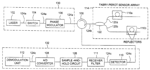
Figure 1 illustrates a fiber-optic time-division multiplexing (TDM)
interferometric
sensor system 100 that incorporates the principles of the present invention.
The
system 100 includes an array 114 of Fabry-Perot sensors 116, a transmitter
unit 130
that produces an interrogation signal for the sensor array 114 and a receiver
unit 132
that receives and demodulates the signals from the sensors. The transmitter
unit 130
includes a laser 102, a switch 104, and a phase modulator 106, while the
receiver unit
132 comprises a detector 110, a receiver filter 111 that suppresses frequency
components in the detected optical signal that are outside the band required
for
demodulation of the sensors, a sample-and-hold circuit 126, an analog to
digital (A/D)
converter 128 and a demodulation unit 112 that extracts the phase of the
individual
sensors 116. The Fabry-Perot sensors 116a and 116b are individually formed on
optical fibers 120a and 120b that are coupled together by a splitter 122
forming a star
network topology. A fiber 124b is connected to a circulator 108 which
separates a lead
fiber into down-lead fibers 124a and up-lead fibers 124c such that the fibers
124a-c
optically couple together elements of the system 100. The fibers 124a, 124b
and 124c
are connected to the circulator so that the interrogation signal from the
transmission
unit 130 is directed towards the sensor array 114 and so the reflected signal
from the
sensor array is directed towards the receiver unit 132. A common lead fiber of
sensor
116a (116b) is formed by the fiber 124b and the portion of the fiber 120a
(120b)
between the coupler 122 and the sensor. Accordingly, a noise contributing
fiber for the
two sensors 116a and 11 6b are formed by the fibers 124b, 120a and 120b.
While Figure 1 illustrates the use of the laser 102 and the phase modulator
106,
the principles of the present invention can be implemented as shown in Figure
1A.
Figure 1A shows a transmitter unit 130 with a frequency shifter 150, such as a
Bragg
cell, which sweeps the frequency of the light from the laser 102.
Additionally, while
9
CA 02535964 2006-02-09
Figures 1 and 1 A show interrogation of Fabry-Perot type interferometers,
principles of
the invention are highly suited for interrogation of other interferometer
types, such as,
for example, Michelson and Mach-Zender based interferometer topologies.
Figure 2 shows aspects of TDM where the laser 102 outputs light with a
periodic
intensity pattern and with a repetition period Tcalled a TDM repetition
period. The
TDM repetition period is divided into transmission time slots of a length
equal to the
sensor delay imbalance zs . A sequence of two or more interrogation pulses are
generated in two or more transmission time slots by switching on and off the
laser 102
directly or by using the switch 104. For the illustrated embodiment, the
repetition period
is divided into five transmission time slots, where time slots one and two are
pulse
transmission time slots while three, four and five are dark transmission time
slots.
The signal of a certain transmission time slot is formed by masking out the
portion of the interrogation signal within the transmission time slot. This is
done by
multiplying the interrogation signal with a signal that is one during the
transmission time
slot and zero in all other time slot. The duty-cycle of the laser 102 is
defined as the
fraction of time in which the laser 102 is turned on. The duty-cycle depends
on the
number of the sensors 116 multiplexed and the separation between the sensors
116.
Pulses propagating a sensor path and a reference path of one of the sensors
116
interfere at the receiver producing optical power amplitudes that depend
periodically on
the phase delay difference between the two paths. The phase delay varies due
to a
response from a measurand.
Figure 3 shows an unwanted reflector R, and first and second reflectors R, and
Rz of the sensor 116 being interrogated. The overlapping pulses reflected from
the
reflectors R, and R2 are reflections of interrogation pulses transmitted in
the same TDM
repetition period, while the pulses reflected from the unwanted reflector RX
are
reflections of interrogation pulses transmitted in another TDM repetition
period. When
the dual-pass delay z between the unwanted reflector R, and one of the
reflectors R,
or R, is equal to a multiple of the TDM repetition period T, pulses reflected
from the
CA 02535964 2006-02-09
unwanted reflector RC and the sensor 116 overlap in time at the receiver and
the
interference between the reflection from the sensor 116 and the unwanted
reflector Rx
may give rise to noise or crosstalk on the demodulated signal from the sensor
116.
Accordingly, unwanted reflectors positioned both before and after the sensor
116 may
give rise to noise and crosstalk on the sensor.
Figure 4 shows that reflections in the common lead fiber 124b leading to
interference between pulses originating from different TDM repetition periods
appear at
positions where the interrogation pulses propagating towards the sensors 116
collide
with the reflected signal from the sensors 116. Weak reflections in the up-
lead fiber
124a and down-lead fiber 124c to a first order approximation do not contribute
to noise
or errors in the detected and demodulated signals. The parts of the common
lead fiber
124b where the pulses collide define collision points 404. Although not shown
in the
figure, there are also collision points on fibers 120a and 120b. The distance
between
the collision points 404 is defined as c 1(2n) - T, where c is the speed of
light and n is the
refractive index of the fiber. This means that the total number of collision
points 404 per
sensor reflector on the common lead fiber 124b is kmaX = LTf l TI, where Tf is
the
maximum difference in delay between a sensor pathway and a noise contributing
pathway. Here, Ld denotes rounding down to the nearest integer. Thus,
suppression of
the interference only requires suppressing the interference between the
reflections from
two interrogation pulses that are less than or equal to kmax TDM repetition
periods
apart.
For z larger than the pulse coherence time, the pulses reflected from the
unwanted reflector R, do not originate from the same repetition period as the
reflectors
R, and R,. This allows for suppression of crosstalk and noise by modulation of
the
phase or frequency of the interrogation pulses from TDM repetition period to
TDM
repetition period so that the interference between the pulses from the
interrogated
sensor 116 and the unwanted pulses does not include frequency components that
are
used to demodulate the sensor 116. By modulating the phase of the
interrogation
11
CA 02535964 2008-04-03
signal, the interference between the signal transmitted in one pulse time slot
and the
signal transmitted in the same or another pulse time slot delayed by more than
the
sensor imbalance provides a frequency outside the frequency bands used for
demodulation of the sensors 116. Furthermore, modulating the phase of the
interrogation signal so that the interference between the signal transmitted
in one pulse
time slot and any signal transmitted in the dark time slots provides a
frequency outside
the frequency bands used for demodulation of the sensors 116 and thus enables
suppression of noise due to leakage during the dark time slots.
The following embodiments described assume that a variant of the two pulse
heterodyne sub-carrier generation is used. However, other embodiments can also
be
used with other interrogation schemes such as phase-generated carrier
interrogation
and multi-pulse heterodyne sub-carrier interrogation.
In one embodiment, the phase difference between the two interrogation pulses
in
the pulse time slots is varied linearly with time so that the sensor phase can
be found
from the sequence of reflected pulses from the sensor 116 by processing
information
within a frequency band centered at the sub-carrier frequency fS, and with a
bandwidth
2BW. The noise or crosstalk due to the interference between an unwanted light
component and a pulse from an interrogated sensor is suppressed if the phase
or
frequency modulation of the interrogation pulses is such that the interference
does not
appear in the frequency band fs, -BW <_ f< f, +BW . Signal components outside
this
frequency band can be removed either by the analog receiver filter 111 (shown
in
Figure 1) or a digital filter within the demodulation unit 112.
In some applications, the interrogation signal may be divided into different
channels that are interleaved in the time domain so that the sampling period
Ts of each
channel is a multiple of the TDM repetition period T. One example of such
interleaving
is the polarization-resolved interrogation method based on switching the
polarization
states of the interrogation pulses described in O.H. Waagaard and E.
ROnnekleiv,
"Method and Apparatus for Providing Polarization Insensitive Signal Processing
for
Interferometric Sensors," U.S. Patent Application Serial No. 10/650,117. In
this
12
CA 02535964 2008-04-03
example, the repetition periods are divided into four polarization channels
that are
defined by the polarization states of the two interrogation pulses. The
polarization
channels are sequentially interrogated so that within P = 4 repetition periods
all
polarization channels are interrogated. In general, the repetition periods may
be
divided into P _ 1 interleaved channels, where P is an integer. The sampling
period for
each interleaved channel becomes T= PT.
The allowed frequencies range can be divided into a low-frequency (f < RBW)
range and a high-frequency range (f > RBW), where RBW is the bandwidth of the
receiver filter 111, which must be larger than 1/(2zs) in order to detect the
individual
pulses.
In one embodiment of the invention where the unwanted interference signal is
shifted to the high-frequency range, the optical frequency is shifted from
repetition
period to repetition period so that the difference in frequency between any
two pulses in
kmaX subsequent TDM repetition periods is larger than RBW. Figure 6 shows how
the
interrogation signal can be shifted in frequency in steps that are larger than
RBW.
Interference between reflected interrogation pulses originating from different
repetition
periods produce frequencies larger than RBW. The receiver filter removes these
interference signals. The required frequency modulation can be achieved by
modulation of the phase using an electro-optical modulator 106 as shown in
Figure 1,
by using a frequency shifter such as an acousto-optical modulator 150 as shown
in
Figure 1A, or by tuning the frequency of the light source. The frequency shift
is reset to
fstep after minimum k. repetition periods.
In Figure 6, the optical frequency shift of leakage light that may occur in
the time
intervals when the intensity nominally should be zero is kept at zero, and it
is therefore
different from the frequency of any of the interrogation pulses. This means
that the
interference between reflected leakage light and reflected interrogation
pulses is also
suppressed since the frequency difference is larger than RBW.
13
CA 02535964 2006-02-09
In another embodiment, the unwanted interference signal is shifted to the low-
frequency range by varying the optical phase of the interrogation pulses from
repetition
period to repetition period in such a manner that the interference between
pulses
reflected from the interrogated sensor and unwanted pulse reflections is
shifted to a
frequency that is outside the frequency band fsc BW that is used for the
demodulation.
The available frequency range to where the unwanted interference signal
components
can be shifted is limited by the sampling period of the individual sampling
channels,
T= PT, and the bandwidth BW of the signal from the interrogated sensor. All
frequency components larger than the receiver Nyquist frequency 1/(2Ts) are
aliased to
the frequency in the range below 1/(2T ) due to the sampled nature of the
pulses and
the receiver sampling. Crosstalk and noise caused by interference between
pulses
reflected from an interrogated sensor and pulses reflected from an unwanted
reflector
are therefore suppressed if the phase modulation between repetition periods is
such
that the unwanted interference signals do not appear at frequencies f in the
ranges
T B W <_ .~ ~ T - .fs, + BW
S S (1)
T +fs~ BW < f <_ T +fS, +BW,
s s
where k is an integer larger than or equal to zero. These bands are the non-
hashed
parts of the frequency axis in figure 5.
The n'th repetition period in a TDM sampling sequence corresponds to the m'th
point in the sampling sequence of the p'th ( p= 0,..., P-1) sampling
(interleaved)
channel so that n= Pm + p. The phase of the interrogation pulses in the first
and
second transmission time slot are
0, (n) = 0,p (m) = 0õs (n) - (2 - ,u)o,, (n) (2a)
0,(n) =0 (m) =0õs(n)+pos, (n), (2b)
14
CA 02535964 2006-02-09
respectively, where 0 _ ,u _ 2 is a constant, ~ns is the modulation that
provides noise
suppression from unwanted reflections and ~5C is the modulation that provides
the sub-
carrier, and they are given by
0õs(n)=On (m)=n-'7cfT=(Pm+p)2 ;TfT (3a)
0, (n)=os,(m)=m)Tj, T +0o l2. (3b)
The phase difference between the two transmission time slots is
¾z (m)-o,p(m)=20, (m)=m27cfs,T +¾o . The freedom to choose ,u in Equations
(2a)
and (2b) enables selection so that the sub-carrier modulation is either on the
first pulse
(,u = 0), on the second pulse (,u = 2) or both (,u =1). Selection of the
frequency f, is
discussed below. If the phase offset of the interleaved channels are chosen as
OOP = p2zfS,T , then 0S,(n) = n;c fT , and the phase difference between the
two
transmission time slots varies linearly with n. The phase offset Oo may be
removed
from the demodulated phase signal by subtraction. In the following
discussions, it is
assumed ¾o = 0 , so that 0 (m) = O5C (m), dp .
The interference between reflectors R, and R2 in interleaved channel p is
given
by
Ip(m)=R,Iz+Rz1,+2Vp(m)~R,RzI,Izcos(m2TCfs, T +Op(m)) (4)
where 11 and 12 are the intensities of the two interrogation pulse, V'' (m) is
the visibility of
the interference and Op(m) is the sensor phase. The complex reflection
response of
interleaved channel p, Xp (m) = t~(m) exp[iO (m)] , where rp (m) = 2V P(m) R,
Rzl,lz , can
be found from the sequence of detected pulses from a sub-carrier with
frequency fs~ .
From the P complex values XP(m), p= 0,...,P-1, the sensor phase can be
calculated.
CA 02535964 2006-02-09
The dual-pass delay between the reflectors R, and Rz is one TDM repetition
period in Figure 3. In order to analyze the interference between the
reflections from R,
, R, and Rr in a more general case, the dual-pass delay difference between the
reflectors R, and RY is set to k = Pj + q (q = 0, 1, ... P-1) times the TDM
repetition
period. Note that the following discussion applies when the dual-pass delay
difference
differs with less than the pulse coherence length from k times the TDM
repetition
period. Pulses reflected from RY appear in the same receiver time slot as the
interference signal from the sensor. There are two unwanted interference
components
within this receiver time slot caused by interference with reflections from
the unwanted
reflector Rx . The first component is caused by the interference between
pulses
originating from the second pulse transmission time slot reflected from the
first reflector
R, and pulses originating from the same pulse transmission time slot reflected
from the
unwanted reflector RY and delayed by k TDM repetition periods. The second
component is the interference between pulses originating from the first pulse
transmission time slot reflected from the second reflector RZ and pulses
originating
from the second pulse transmission time slot and delayed by k TDM repetition
periods
reflected from the unwanted reflector RX . The interference phase of these two
components can be expressed as,
0 p(m)-0z '(m-j)+O~(m)+O (m)
=0ns(n)-0õs(n-k)+,uos, (m)-pos, (m-j)+OY (m)+Of (m)
=[n2 -(n-k)2 ])Tf,T+,u[m-(m- j)];Tfs,T +OP (m)+Os (m) (5a)
=mk27cf,T +OP(m)+OP(m)-ak +,u,8,
Y,p(m)-0p-9(m-I)+0p(m)
=0õs(n)-0õs(n-k)-(2-,u)os, (m)-uos, (m-j)+6. (m)
=[n' -(n-k)'];T f,T+[-(2-,u)m-p (m-J)]TCfs, T +0 P (m) (5b)
=mk27cf,T -m27tfj, +0p(m)-a~ +
16
CA 02535964 2006-02-09
Here, ak =k(k+2p);cf,T,,(3,= j;Tf,T, and OP(m) is the phase delay difference
between the second reflector R. and the unwanted reflector Rr .0,P(m) is
assumed to
be slowly varying comparable to the receiver Nyquist frequency. Thus, the
interference
components in (5a) and (5b) are confined to frequency bands centered around
kf, and
fs, - kf;=
While not shown in the figures, noise and crosstalk can also appear if the
dual-
pass delay between the second reflector R, and the unwanted reflector R, is
equal to k
= Pj + q (q = 0, 1, ... P-1) times the TDM repetition period. In this case,
the signal from
the sensor includes the interference between pulses originating from the
second pulse
transmission time slot reflected from the first reflector R, and pulses
originating from the
first pulse transmission time slot reflected from the unwanted reflector Rx
and the
interference between pulses originating from the first pulse transmission time
slot
reflected from the second reflector R2 and pulses originating from the first
pulse
transmission time slot reflected from the unwanted reflector RC . The phase of
these
two interference components is given as,
Op(m)-K' (m-j)+Of (m)+0" (m)
=~6õs(n)-0,,s(n-k)+,uos, (m)+(2-,u)os, (m- j)+0P(m)+Of (m)
_ [n' - (n - k)2 ]7rf,T +[,um +(2 -,u)(m - j)];z fsTs +Op (m)+OP(m) (6a)
= mk2;TfTs +m2;Tfs,Ts +O (m)+Os (m)-ak -(2-,u)~j
O,p (m) - OP-q (m - j ) + Op (m)
=Oõs(n)-0õs(n-k)-(2-,u)os, (m)+,uos, (m-j)+0r (m)
= [n' - (n - k)2 ];Tf,T + (2 -,u)[-m + (m - j)]27t fs, T + OY (m) (6b)
=mk27tf,T +OP(m)-ak -(2-,u)~3j.
In this case, the two interference components are confined to frequency bands
centered around kf, and f , + kf, .
17
CA 02535964 2006-02-09
The two collision points with delays that differ by k times the TDM repetition
period from the delays of R, and R2 give rise to components in the detected
signal at
beat frequencies kf,, f5f -kf, and f, +kf, . Beat frequencies that are larger
than 1/(2Ts)
are aliased. In a preferred embodiment, the subcarrier frequency is chosen as
fs'; =
1/(NPTS), where Np is an integer larger than 2. After aliasing to the Nyquist
frequency
range [0,1 /(2T )), the beat signal frequencies become,
f, (k)=Imod(kf,+Nfs, l2,Npfs,)-Npfs, /2)1 (7a)
.fb (k) = Imod(.fs, - kf, + NP.fs, l 2, Np.fs,)- NP.fs, l 2)I (7b)
f~ (k) = Imod(.fS, + kf, + NP.fs, l 2, Np.fS,)- Np fs~ l 2)~ (7c)
f, should be chosen such that neither f~ (k), fb(k) nor f(k), k = 1, 2, ...
kmax
appears in the frequency range between fS,. - BW and fs, + BW. The separation
between fsc and the beat frequency that is closest to fs, is defined as fSep.
In general,
fSep should be as large as possible to avoid overlap between the beat signal
band and
the subcarrier band. The choice of frequency f, that gives the largest
possible value
for fsep is found by setting fa(kn,ax +1) = fS~ in Equation (7a). This
equation has solutions
f, = lfSep where l<- kn,ax is an integer that has no common divisor with kmax
+1, and
.~sep = k .f s + l = [(kmax + 1)NpT ]-~ (8)
max
Accordingly, fs~p is maximum if Np is as small as possible, i.e., NP = 3
should be
chosen.
Figure 7 shows generated beat frequencies due to interference between the
reflection from the collision points and the reflection from the sensor with
k,,ax =16 and
Np = 3. With l=1, the frequencies that are closest to f, are fb(1) , fJ1) ,
fb(kn,ax) and
18
CA 02535964 2006-02-09
f(kmax) . In some cases, it might be preferable to move fb(1) and ffl) further
away
from f, This is achieved by selecting 1> 1.
The interference between the leakage light reflected from another time-
division
multiplexed sensor and reflection of the interrogation pulses from the
interrogated
sensor can also be suppressed by modulating the difference between the phase
of the
pulse transmission time slots and the phase of the dark transmission time
slots, Ooff .
By setting Ooff (n) =Oõs (n) and using Equation (2), the phase of the
interference between
the first or second pulse generated in TDM repetition period n, respectively,
and the
leakage light generated in TDM repetition n-k may be expressed as
0, (n)-0o~(n-k)+O, (n)=Ons(n)-Ons(n-k)-(2-,u)os, (n)+0, (n) =mk2~Ts -(2-
,u)m~fS,Ts +0
C~(n)+ak (9a)
02 (n)-0o~-(n-k)+0.Y2(n) =0ns(n)-Oõ5(n-k)+,uOs, (n)+OX2(n)
= mk2)7fT + fimy~,T s +0r2(n)+ak
(9b)
where 0r1(n) and 0x2(n) are the physical phase difference between the
interfering
components and ak is the same as in Equations (5a) and (5b). It is possible to
choose
p and f, so that the interference between signals received from the
interrogated sensor
and leakage light that has propagated pathways of other time-division
multiplexed
sensors or other pathways with moderate transmission loss appears at a
frequency
different from the sub-carrier frequency fS,. In most cases the difference in
delay
between the time-division multiplexed sensors is less than the TDM repetition
period.
The interference between the leakage light and the interrogation pulses from
the same
TDM period (k=0) appears at a frequencies ,ufs, and (2 -,u) fs, which is
different from fs,
when ,u is different from 0 or 2. Note that the interference between
interrogation pulses
and leakage light can be suppressed also when O~~ (n) =Ons (n) = 0, i.e., no
modulation
is applied to suppress interference between pulses originating from different
TDM
repetition periods. In a preferred embodiment, ,u =1 may be chosen so that
19
CA 02535964 2006-02-09
(n)=0õs(n)-0s, (n) (10a)
0, (n)=Ons(n)+0s, (n). (10b)
Then, the interference between the leakage and the interrogation pulses from
the same
TDM repetition period appears at half the sub-carrier frequency. If fs, > 4
BW, the
interference between the interference pulses and the leakage light does not
give any
contribution in the signal band from which the sensor phase is extracted, and
can
therefore be filtered out by any appropriate digital filter.
With the phase modulation scheme described in Equations (9) and (10), 0S, must
be modulated two sub-carrier periods before the phase can be reset. This means
that
the maximum voltage applied to the phase modulator is twice the maximum
voltage
when the crosstalk due to leakage is not suppressed. However, ¾S, can be reset
every
sub-carrier period if a square wave pattern with period that is half the sub-
carrier period
and amplitude 7r / 2 to is added to Oofr :
0off (n) (n) + - rect( n ), (11)
2 2PNp
where
rect(x)= 1 x-Lxj<0.5 (12)
-1 otherwise.
Thus, the reset of OS,(n) is compensated by a phase shift of 'T in ooff,
leading to an
interference signal between the leakage light and one of the two pulses that
are
periodic with half the sub-carrier period.
While the foregoing is directed to embodiments of the present invention, other
and further embodiments of the invention may be devised without departing from
the
basic scope thereof, and the scope thereof is determined by the claims that
follow.