Note: Descriptions are shown in the official language in which they were submitted.
CA 02536119 2006-02-13
MICRO-SWITCHES FOR DOWNHOLE USE
BACKGROUND
The invention relates to micro-switches for use in various tools, such as
downhole
well tools.
In forming a well, many different types of operations may be performed,
including drilling, logging, completion, and production operations. Various
different
types of devices are used to perform the desired operations. Examples of such
devices
include perforating guns to perform perforating operations, flow control
devices to
control fluid flow (injection or production), packers to isolate different
regions of the
well, and other devices.
The activating mechanisms to activate such devices may include mechanical,
hydraulic, and electrical activating mechanisms. To electrically activate a
downhole
device, a power source is connected to the downhole device. This is typically
accomplished by using switches, either at the surface or in a downhole module.
The
switch is initially open to isolate the power source from the downhole device.
When
activation is desired, the switch is closed to provide electrical power to the
downhole
device.
In wellbore applications, one type of switch is made from a gas discharge tube
that is either a triggered type of over-voltage type switch. A triggered-type
switch
employs an external stimulus to close the switch or to activate it. An over-
voltage switch
is activated whenever the voltage level on one side of the switch exceeds a
threshold
value.
Some switches employ a gas tube having an electrode at each end. In order to
make the switch conduct, either a trigger voltage is applied to a third
internal grid or
anode, or the switch is forced into conduction as a result of an over-voltage
condition.
Because the typical gas tube discharge switch is arranged in a tubular
geometry, it is
usually associated with a relatively high inductance. Also, the tubular shape
of a gas tube
does not allow convenient reduction of the overall size of a switch.
Additionally, it may
be difficult to integrate the gas tube switch with other components.
CA 02536119 2006-02-13
2
Another type of switch includes an explosive shock switch. The shock switch is
constructed using a flat flexible cable having a top conductor layer, a center
insulator
layer, and a bottom conductor layer. A small explosive may be detonated on the
top layer
causing the insulator layer to form a conductive ionization path between the
two
conductor layers. One variation of this is a "thumb-tack" switch in which a
sharp metal
pin is used to punch through the insulator layer to electrically connect the
top conductive
layer to the bottom conductive layer.
The explosive shock switch offers a low inductance switch but an explosive
pellet
must ignite to trigger the switch. The thumbtack switch is similar to the
explosive switch
but it may not be reliable. Thus, a need continues to exist for switches
having improved
reliability and triggering characteristics.
SUMMARY
In general, according to one embodiment, an apparatus for use in a downhole
tool
includes a downhole component, and a switch including conductors and a
microelectromechanical device adapted to electrically connect the conductors
when
activated.
Other features and embodiments will become apparent from the following
description, from the drawings, and from the claims.
BRIEF DESCRIPTION OF THE DRAWINGS
Fig. 1 illustrates an embodiment of a tool string for use in a wellbore.
Fig. 2 is a schematic diagram of an exploding foil initiator (EFI) trigger
circuit in
accordance with an embodiment useable in the tool string of Fig. 1.
Fig. 3 illustrates an embodiment of a switch including a
microelectromechanical
tack.
Figs. 4A-4B illustrates another embodiment of a switch having an electrode
tethered by a frangible element.
Fig. 5 illustrates yet another embodiment of a switch having parallel plates
and a
dielectric layer capable of breaking down in response to an applied electrical
current.
Fig. 6 illustrates a further embodiment of a switch including a bistable
element.
CA 02536119 2006-02-13
3
Figs. 7A-7D illustrate yet a further embodiment of a switch that includes a
chamber containing a dielectric gas.
Fig. 8 illustrates another embodiment of a switch including a moveable
electrode.
DETAILED DESCRIPTION
In the following description, numerous details are set forth to provide an
understanding of the present invention. However, it will be understood by
those skilled
in the art that the present invention may be practiced without these details
and that
numerous variations or modifications from the described embodiments may be
possible.
For example, although reference is made to switches used for activating
exploding foil
initiators (EFIs), further embodiments may include switches used to activate
other
components.
As used here, the terms "up" and "down"; "upper" and "lower"; "upwardly" and
downwardly"; "above" and "below"; and other like terms indicating relative
positions
above or below a given point or element are used in this description to more
clearly
described some embodiments of the invention. However, when applied to
equipment and
methods for use in wells that are deviated or horizontal, or when such
equipment are at a
deviated or horizontal orientation, such terms may refer to a left to right,
right to left, or
other relationship as appropriate.
Referring to Fig. l, a downhole tool 10, which may include a perforating gun
15
as one example, is lowered through a tubing 7 positioned in a wellbore 8 that
is lined with
a casing 9. A packer 6 is set between the tubing 7 and the casing 9 to isolate
the tubing-
casing annulus. The downhole tool 10 is run on a carrier 12, which may be a
wireline,
slickline, tubing, or other carrier. Certain types of carriers 12 (such as
wirelines) may
include one or more electrical conductors 13 over which power and signals may
be
communicated to the downhole tool 10. The perforating gun 15 shown in Fig. 1
includes
a plurality of shaped charges 20. In one embodiment, such shaped charges 20
may be
detonated by use of initiator devices 22 that are activated by a command
issued from the
well surface, which may be in the form of electrical signals sent over the one
or more
electrical conductors 13 in the carrier 12. Alternatively, the command may be
in the form
CA 02536119 2006-02-13
4
of pressure pulse commands or hydraulic commands. The initiator devices 22 may
be
electrically activated by signals communicated over one or more electrical
lines 24.
Other embodiments of the downhole tool 10 may include packers, valves, plugs,
cutters, or other devices. Thus, in these other embodiments, the command
issued from
the well surface may activate control modules to set packers, to open and
close valves, or
to actuate or release other devices. To activate a device in the downhole tool
10, switches
may be provided to connect an electrical signal or electrical power to the
device. For
example, to initiate an explosive, the initiator device 22 may include a
switch and an
exploding foil initiator (EFI) circuit.
In accordance with some embodiments, switches may include
microelectromechanical elements, which may be based on microelectromechanical
system (MEMS) technology. MEMS elements include mechanical elements which are
moveable by an input energy (electrical energy or other type of energy). MEMS
switches
may be formed with micro-fabrication techniques, which may include
micromachining
on a semiconductor substrate (e.g., silicon substrate). In the micromachining
process,
various etching and patterning steps may be used to form the desired
micromechanical
parts. Some advantages of MEMS elements are that they occupy a small space,
require
relatively low power, are relatively rugged, and may be relatively
inexpensive.
Switches according to other embodiments may be made with microelectronic
techniques similar to those used to fabricate integrated circuit devices. As
used here,
switches formed with MEMS or other microelectronics technology may be
generally
referred to as "micro-switches." Elements in such micro-switches may be
referred to as
"micro-elements," which are generally elements formed of MEMS or
microelectronics
technology. Generally, switches or devices implemented with MEMS technology
may be
referred to as "microelectromechanical switches."
In one embodiment, micro-switches may be integrated with other components,
such as EFI circuits to initiate explosives. Integrated components are
contained in
smaller packages, which enable more efficient space utilization in a wellbore.
As used
here, components are referred to as being "integrated" if they are formed on a
common
support structure placed in packaging of relatively small size, or otherwise
assembled in
close proximity to one another. Thus, for example, a micro-switch may be
fabricated on
CA 02536119 2006-02-13
the same support structure as the EFI circuit to provide a more efficient
switch because of
lower effective series resistance (ESR) and effective series inductance (ESL).
The micro-
switch may also be formed on a common substrate with other components.
Referring to Fig. 2, according to one embodiment, a capacitor discharge unit
(CDU) includes a capacitor 202 that is chargeable to a trigger voltage level.
The
capacitor 202 provides a local energy source to provide activating energy. The
capacitor
202 is connected to a micro-switch 204 that may be activated closed by a
trigger voltage
Vu;gge~ or trigger current I~;gger. When the switch 204 is closed, activating
energy is
coupled to an EFI circuit 206 to activate the EFI 206.
An EFI circuit typically includes a metallic foil connected to a source of
electric
current, such as the capacitor 202. A reduced neck section having a very small
width is
formed in the foil, with an insulator layer placed over a portion of the foil
including the
neck section. When a high current is applied through the neck section of the
foil, the
neck section explodes or vaporizes. This causes a small flyer to shear from
the insulator
layer, which travels through a barrel to impact an explosive to initiate a
detonation.
The following describes various embodiments of micro-switches. Such micro-
switches are useable in the CDU of Fig. 2, or alternatively, they may be used
to connect
electrical energy to other downhole components.
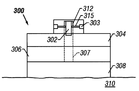
Refernng to Fig. 3, according to an embodiment, a MEMS switch 300 is acdvable
by a MEMS tack 302. In this embodiment, the MEMS tack 302 replaces the
thumbtack
actuator used in some conventional thumbtack switches. The switch 300 includes
top and
bottom conductor layers 304 and 308 that sandwich an insulating layer 306. The
conductors 304 and 308 may each be formed of a metal or some other suitable
conductive
material. The insulator layer 306 may include a polyimide layer, as an
example. The
MEMS tack 302 may be placed over the top conductor layer 304. When actuated,
such
as by an applied trigger voltage V~;~e~ having a predetermined amplitude, an
actuator 303
releases the MEMS tack 302 to move through the layers 304 and 306 to contact
the
bottom conductor layer 308. This electrically couples the top and bottom
conductors 304
and 306 to activate the switch 300. Thus, the electrically conductive layer
304 may be
driven to a drive voltage Vdrive~ while the electrically conductive layer 308
is connected to
the component to be activated (e.g., the EFI circuit 206 of Fig. 2).
CA 02536119 2006-02-13
6
In one embodiment, a preformed bore 307 may already be present in the layers
304 and 306 through which the MEMS tack 302 may travel. In another embodiment,
the
MEMS tack 302 may have a sharp tip to puncture through the layers 304 and 306
to
reach the layer 308.
In one arrangement, the actuator 303 includes moveable support elements 305
that
support the tack 302 at an enlarged flange portion 312. The support elements
305 when
withdrawn from the tack flange portion 312 allow the tack 302 to drop into the
bore 307.
The support elements 305 may be radially moveable by a MEMS gear mechanism
303.
When an electrical energy is applied, the MEMS gear mechanism 303 radially
retracts the
support elements 305 from the tack 302 to enable it to drop into the bore 307
to
electrically connect the conductors 304 and 308. In an alternative
arrangement, instead
of retracting the support from the tack 302, a MEMS gear mechanism 303 may be
employed to drive the tack 302 into the bore 307.
The layered structure making up the micro-switch 300 may be formed on a
substrate 310, which may be a semiconductor, insulator, or other substrate. In
one
example, the substrate 310 may be a silicon substrate. The conductor layer 308
is first
deposited on the substrate 310, followed by the insulator layer 306 and the
next
conductor layer 304. The bore 307 may be patterned by an anisotropic etch
through the
layers 304 and 306. The MEMS structure including the tack 302 and the actuator
303
may then be formed on top of the conductor layer 304 over the bore 307.
Referring to Figs. 4A-4B, according to another embodiment, a micro-switch 500
includes a first substrate 502 and a second substrate 504. The first substrate
502 and the
layers formed over it are actually shown upside down in Figs. 4A-4B. In
forming the
micro-switch 500, the two substrates 502 and 504 are independently patterned,
with one
flipped upside down to face the other one.
An insulator layer 506 (e.g., a nitrite or SXNy layer) is formed over a
surface of the
substrate 502. A conductive line 510 (e.g., a metal layer including aluminum,
nickel,
gold, copper, tungsten, and titanium) is formed on the insulator layer 506. A
plurality of
tethers 516, each made of a semiconductor material such as doped silicon of
selected
resistivity, may then be formed on the substrate 502 for supporting a
conductive plate
514, which may be made of a metal such as aluminum, nickel, gold, copper,
tungsten,
... I ~ . Ii
CA 02536119 2006-02-13
7
and titanium. The tethers S 16 are bonded to the conductive plate 514 at the
contact
points between the tethers 516 and plate 514. The tethers 516, when exposed to
a
relatively large electrical current, disintegrates or otherwise breaks to
allow the
conductive plate 514 to drop through the gap 515 to contact a conductive layer
512
formed over the substrate 504. Thus, effectively, the tethers 516 are
frangible elements
that break apart in response to application of an electrical voltage or
current.
As shown in Fig. 4B, the tethered plate 514 has a bent portion 517 that allows
it to
be connected to a bond pad 519 formed over the substrate 502. The bond pad 519
may
be contacted to a lead finger, for example, that provides a drive voltage
Vdrive to the
tethered conductive plate 514. The tethers 516 are contacted to the conductive
line 510,
which in turn may be connected to another bond pad 521 that receives a trigger
current
Itrigger~
In operation, the conductive plate 514 is driven to a drive voltage Vari"e.
When
the micro-switch 500 is to be closed (or activated), a trigger current IUigger
is applied
through the conductive line 510, which breaks or disintegrates at least a
portion of the
tethers 516. This allows the conductive plate 514 (which is at the drive
voltage Vdrive) to
drop to contact the conductive layer 512, thereby driving the voltage Vo to
the drive
voltage Vdrive~ 'tee conductive layer 512 (and the voltage Vo) may be
connected to a
device to be activated, such as the EFI circuit 206 of Fig. 2.
Refernng to Fig. 5, yet another embodiment of a micro-switch 600 includes two
parallel plates 602 and 604 with a dielectric layer 610 between the parallel
plates. The
dielectric properties of the dielectric layer 610 can be modulated by an
electrical energy
in the form of a trigger voltage or current to provide a conductive path
between the two
conductive plates 602 and 604. A conductive line 606 may be formed over the
conductive plate 604, with an insulator layer 607 between the line 606 and
conductive
plate 604. The dielectric layer 610 separating the conductive plates 602 and
604 may be
a dielectric solid, liquid, or gas. The line 606 when supplied with a trigger
current causes
the dielectric layer 610 to break down and provide a conductive path between
the
conductive plates 602 and 604.
In operation, a drive voltage Vdrive is applied to the conductive plate 602
with the
conductive plate 604 coupled to a device to be activated. When a trigger
current Iui~er is
CA 02536119 2006-02-13
applied to the line 606, the dielectric layer 610 breaks down and the voltage
V~;"e is
conducted through the conductive path from the conductive plate 602 to the
plate 604 to
raise the voltage Vo to the drive voltage V~;"e.
Referring to Fig. 6, a micro-switch 700 according to another embodiment
includes
a bistable microelectromechanical switch 700. The switch 700 includes a
contact plate
706 that is maintained at a neutral position (i.e., inactive position) when a
drive voltage
Vdrive is applied. The contact plate 706 is positioned at substantially a mid-
plane between
plates 702 and 704. The plates 702 and 704 are each driven to Vap,,e to
maintain the
contact plate 706 at its neutral position. When activation of the micro-switch
700 is
desired, a trigger voltage V~;~ger is added to one of the plates 702 and 704
to increase the
voltage to Vdri~e + Va;gger This creates an electrostatic force to cause an
imbalance in the
switch, which moves the plate 706 to contact the plate 704. The contact plate
706 at its
base end is attached to a support column 710. In one embodiment, the contact
plate 706
and support column are integrally formed with a metal to provide a cantilever.
The
cantilever is adapted to bend by application by an electrostatic force. When
the
cantilever plate 706 contacts the plate 704, the voltage Vdrive '~ Vrrigger is
communicated to
the cantilever plate 706.
Referring to Fig. 7A-7D, another embodiment of a micro-switch 800 is
illustrated.
Fig. 7A is an exploded side view of the micro-switch 800, including a top
substrate 802
and a bottom substrate 804. Structures may be formed on each of the substrates
802 and
804. Fig. 7B shows a top view of the bottom substrate 804, and Fig. 7C shows a
bottom
view of the top substrate 802. A conductive plate 806 and an upper dielectric
layer 810
are deposited on the top substrate 802. A lower conductive plate 808 is formed
over the
bottom substrate 804, and a lower dielectric layer 812 is formed over the
lower
conductive plate 808. In addition, a triggering electrode 814 is formed over
the dielectric
layer 812.
As shown in Fig. 7C, the dielectric layer 810 has a portion cut away to form a
window exposing the upper conductive plate 806. Similarly, as shown in Fig.
7B, the
dielectric layer 812 has a portion cut away to form a window exposing the
lower
conductive plate 808.
, .., i ~" ,
CA 02536119 2006-02-13
9
As shown in Fig. 7A, the upper substrate 802 is flipped to an upside down
position. When the upper and lower substrates 802 and 804 and attached
structures are
contacted to each other, the structure of Fig. 7D is achieved. The fabrication
of the
structure may be performed in a chamber filled with inert gas (e.g., Argon) so
that the
gap 816 formed as a result of bringing the two substrates 802 and 804 together
is also
filled with the inert gas. Alternatively, the gap 816 may be filled with
another dielectric
element, such as a liquid or solid dielectric. The dielectric material is
selected to break
down upon application of a predetermined voltage or current trigger signal.
In operation, a trigger voltage is applied to the trigger conductor plate 814
that
breaks down the insulator in the gap 816 to provide a conductive path between
the upper
conductive plate 806 and the lower conductive path 808, thereby closing the
micro-
switch 800.
Referring to Fig. 8, according to another embodiment, a MEMS switch 400 may
include electrical contacts 404, 406, 408, and 410 separated by gaps 420 and
422.
Contacts 404 and 406 are electrically coupled to lines 416 and 418,
respectively, which
terminate at electrodes 412 and 414, respectively. The electrodes 412 and 414
may be
electrically contacted to corresponding components, such as to an energy
source and a
device to be activated by the energy source. The contacts 404 and 406 are
slanted to abut
against contacts 408 and 410, respectively, when the contacts 408 and 410 are
moved
upwardly by an actuator member 402. The actuator member 402 may be moveable by
application of a trigger voltage, for example. When the contacts 404, 406,
408, and 410
are contacted to one another, an electrically conductive path is established
between the
electrodes 412 and 414. Movement of the actuator member 402 may be
accomplished by
using MEMS gears (not shown).
The contacts 404, 406, 408, and 410 may be formed of metal or some other
electrically conductive material. The switch 400 may be formed in a
semiconductor
substrate, such as silicon.
Advantages of the various switches disclosed may include the following.
Generally, the switches may be implemented in relatively small assemblies,
which
improves the efficiency of the switches due to reduced resistance and
inductance.
Further, some of the switches may be integrated with other devices, such as
EFI circuits,
CA 02536119 2006-02-13
1U
to form an overall package that is reduced in size. Reliability and safety of
the switches
are enhanced since explosives or mechanical actuation as used in some
conventional
switches are avoided.
While the invention has been disclosed with respect to a limited number of
embodiments, those skilled in the art will appreciate numerous modifications
and
variations therefrom. It is intended that the appended claims cover all such
modifications
and variations as fall within the true spirit and scope of the invention. For
example, other
switch configurations using micro-elements may be used.