Note: Descriptions are shown in the official language in which they were submitted.
CA 02536641 2006-02-22
WO 2005/027444 PCT/US2004/029863
TX LINE DRIVER WITH COMMON MODE IDLE STATE AND SELECTABLE
SLEW RATES
BACKGROUND OF THE INVENTION
TECHNICAL FIELD OF THE INVENTION
This invention relates generally to communication
systems and more particularly to line driver circuits used
therein.
1o DESCRIPTION OF RELATED ART
Communication systems are known to transport large
amounts of data between a plurality of end user devices,
which, for example, include telephones, facsimile machines,
computers, television sets, cellular telephones, personal
digital assistants, etc. As is also known, such
communication systems may be local area networks (LANs)
and/or wide area networks (WANs) that are stand-alone
communication systems or interconnected to other LANs
and/or WANs as part of a public switched telephone network
~o (PSTN), packet switched data network (PSDN), integrated
service digital network (ISDN), or Internet. As is further
known, communication systems include a plurality of system
equipment to facilitate the transporting of data. Such
system equipment includes, but is not limited to, routers,
switches, bridges, gateways, protocol converters, frame
relays, private branch exchanges, etc.
The transportation of data within communication
systems is governed by one or more standards that ensure
the integrity of data conveyances and fairness of access
3o for data conveyances. For example, there are a variety of
Ethernet standards that govern serial transmissions within
a communication system at data rates of 10 megabits per
second, 100 megabits per second, 1 gigabit per second and
beyond. Synchronous Optical NETwork (SONET), for example,
1
CA 02536641 2006-02-22
WO 2005/027444 PCT/US2004/029863
requires 10 gigabits per second. In accordance with such
standards, many system components and end user devices of a
communication system transport data via serial transmission
paths. Internally, however, the system components arid end
s user devices process data in a parallel manner. As such,
each system component and end user device must receive the
serial data and convert the serial data into parallel data
without loss of information.
Accurate recovery of information from high-speed
to serial transmissions typically requires transceiver
components that operate at clock speeds equal to or higher
than the received serial data rate. Higher clock speeds
limit the usefulness of prior art clock recovery circuits
that require precise alignment of signals to recover clock
s5 and/or data. Higher data rates require greater bandwidth
for a feedback loop of the recovery circuits to operate
correctly. Some prior art designs are bandwidth limited.
As the demand for data throughput increases, so do the
demands on a high-speed serial transceiver. The increased
2o throughput demands are pushing some current integrated
circuit manufacturing processes to their operating limits,
where integrated circuit processing limits (e. g., device
parasitics, trace sizes, propagation delays, device sizes,
etc.) and integrated circuit (IC) fabrication limits (e. g.,
25 IC layout, frequency response of the packaging, frequency
response of bonding wires, etc.) limit the speed at which
the high-speed serial transceiver may operate without
excessive fitter performance and/or noise performance.
A further alternative for high-speed serial
3o transceivers is to use an IC technology that inherently
provides for greater speeds. For instance, switching from
a Complementary Metal Oxide Semiconductor (CMOS) process to
a silicon germanium or gallium arsenide process would allow
integrated circuit transceivers to operate at greater
2
CA 02536641 2006-02-22
WO 2005/027444 PCT/US2004/029863
speeds, but at substantially increased manufacturing costs.
CMOS is more cost effective and provides easier system
integration. Currently, for most commercial-grade
applications, including communication systems, such
alternate integrated circuit fabrication processes are too
cost prohibitive for wide spread use.
Modern communication systems, including high data rate
communication systems, typically include a plurality of
circuit boards that communicate with each other by way of
so signal traces, bundled data lines, back planes, etc.
Accordingly, designers of high data rate communication
transceiver devices often have conflicting design goals
that relate to the performance of the particular device.
For example, there are many different communication
protocols specified for data rates that range from 2.48832
gigabits per second for OC48, to 9.95 gigabits per second
for OC192. Other known standards define data rates of 2.5
gigabits per second (INFINIBAND) or 3.125 gigabits per
second (XAUI). These different data rates affect the
2o allowable rise and fall time of the signal, the peak
amplitude of the signal and the response time from an idle
state. For example, one protocol may specify a peak
voltage range of 200-400 millivolts, while another standard
specifies a mutually exclusive voltage range of 500-700
.millivolts. Thus, a designer either cannot satisfy these
mutually exclusive requirements or must design a high data
rate transceiver device that can adapt according to the
protocol being used for the communications.
Along these lines, field programmable gate array
(FPGA) circuits are gaining in popularity for providing the
required flexibility and adaptable performance described
above for those designers that seek to build one device
that can operate according to multiple protocols. Thus,
while FPGA technology affords a designer an opportunity to
3
CA 02536641 2006-02-22
WO 2005/027444 PCT/US2004/029863
develop flexible and configurable hardware circuits,
specific designs that achieve the desired operations must
still be developed. For example, based on a transceiver's
transmission rate, it is desirable to provide a transceiver
design with an adaptive slew rate. Similarly, because
response times may be very limited, especially for the
higher data rate communication protocols, it is desirable
to minimize a rise time from an idle state to an
operational state. Accordingly, there is a need for an
so idle state mode of operation that reduces settle time and
enables the transceiver device to produce a signal quickly.
BRIEF SUMMARY OF THE INVENTION
The present invention includes a transmit (Tx) line
15' driver having a selectable slew rate and a common idle
state mode and further including circuitry for selecting
the slew rate and for placing the transmit line driver in
the common idle state mode. A transmit line driver,
generally includes a pre-driver circuit that provides an
2o input data stream to a current driver. The current driver
then produces a corresponding output data stream at a
specified current level that is sufficient to drive an
output channel, circuit, etc. Coupled to a differential
line carrying the input data stream is a plurality of
25 selectable capacitors of a selectable capacitor array.
Accordingly, the circuitry selects capacitors of the
selectable capacitor array to calibrate a slew rate for the
input data stream and, accordingly, for the output data
stream produced by the current driver.
3o The circuitry further is coupled to select a switch to
ground or remove a bias signal from the pre-driver circuit,
and more specifically, a bias signal from a biasing device
of the pre-driver circuit to prompt the pre-driver circuit
to provide an output voltage of VDD (source voltage) to a
4
CA 02536641 2006-02-22
WO 2005/027444 PCT/US2004/029863
pair of inputs of the current driver whenever a. transmitter
is in an idle state and is not producing an output data
stream. The output voltage, which is coupled as an input
of the current driver, causes the current driver to produce
an output voltage that is at a specified level. In the
described embodiment of the invention, responsive to device
characteristics and resistor values of a resistor coupled
between a drain and the source voltage, the output voltage
of the current driver is at a specified level that is one
Zo half of a logic one value for the output data stream.
BRIEF DESCRIPTION OF THE DRAWINGS
Figure 1 is a schematic block diagram of a
programmable logic device that includes programmable logic
fabric, a plurality of programmable multi-gigabit
transceivers (PMGTs) and a control module;
Figure 2 is a schematic block diagram of one
embodiment representing one of the programmable multi-
gigabit transceivers;
2o Figure 3 illustrates an alternate schematic block
diagram representing one of the programmable multi-gigabit
transceivers;
Figure 4A illustrates a schematic block diagram of a
programmable receive PMA module that includes a
~5 programmable front-end, a data and clock recovery module,
and a serial-to-parallel module;
Figure 4B illustrates a schematic block diagram of a
programmable transmit PMA module that includes a phase
locked loop, a parallel-to-serial module, and line driver;
3o Figure 5 is a functional schematic diagram of a line
driver with selectable slew rates and a common idle state
mode of operation according to one embodiment of the
invention;
5
CA 02536641 2006-02-22
WO 2005/027444 PCT/US2004/029863
Figure 6 is a functional schematic diagram that
illustrates a first mode of operation of a Tx line driver
formed according to one embodiment of the invention;
Figure 7 is a functional schematic diagram that
illustrates a second mode of operation of a Tx line driver
formed according to one embodiment of the invention;
Figure 8 is a signal diagram showing a logic one
signal transmitted at two different rates and the
corresponding slew rates; and
to Figure 9 is a flow chart illustrating operation of the
present invention according to one embodiment of the
present invention.
DETAILED DESCRIPTION OF THE INVENTION
Figure 1 is a schematic block diagram of a
programmable logic device 10 that includes programmable
logic fabric 12, a plurality of programmable multi-gigabit
transceivers (PMGTs) 14-28 and a control module 30. The
programmable logic device 10 may be a programmable logic
~o array device, a programmable array logic device, an
erasable programmable logic device, and/or a field
programmable gate array (FPGA). When the programmable
logic device 10 is an FPGA, the programmable logic fabric
12 may be implemented as a symmetric array configuration, a
row-based configuration, a sea-of-gates configuration,
and/or a hierarchical programmable logic device
configuration. The programmable logic fabric 12 may
further include at least one dedicated fixed processor,
such as a microprocessor core, to further facilitate the
so programmable flexibility offered by programmable logic
device 10.
The control module 30 may be contained within the
programmable logic fabric 12 or it may be a separate
module. In either implementation, the control module 30
6
CA 02536641 2006-02-22
WO 2005/027444 PCT/US2004/029863
generates the control signals to program each of the
transmit and receive sections of the programmable multi-
gigabit transceivers 14-28. In general, each of the
programmable multi-gigabit transceivers 14-28 performs a
serial-to-parallel conversion on received data and performs
a parallel-to-serial conversion on transmit data. The
parallel data may be 8-bits, 16-bits, 32-bits, 64-bits,
etc.
Typically, the serial data will be a 1-bit stream of
so data that may be a binary level signal, multi-level signal,
etc. Further, two or more programmable multi-gigabit
transceivers may be bonded together to provide greater
transmitting speeds. For example, if PMGTs 14, 16 and 18
are transceiving data at 3.125 gigabits-per-second, the
PMGTs 14-18 may be bonded together such that the effective
serial rate is 3 times 3.125 gigabits-per-second.
Each of the programmable multi-gigabit transceivers
14-28 may be individually programmed to conform to separate
standards. In addition, the transmit path and receive path
of each programmable mufti-gigabit transceivers 14-28 may
be separately programmed such that the transmit path of a
transceiver is supporting one standard while the receive
path of the same transceiver is supporting a different
standard. Further, the serial rates of the transmit path
and receive path may be programmed from 1 gigabit-per-
second to tens of gigabits-per-second. The size of the
parallel data in the transmit and receive sections, or
paths, is also programmable and may vary from 8-bits, 16-
bits, 32-bits, 64-bits, etc.
3o Figure 2 is a schematic block diagram of one
embodiment representing one of the programmable multi-
gigabit transceivers 14-28. As shown, the programmable
mufti-gigabit transceiver includes a programmable physical
media attachment (PMA) module 32, a programmable physical
7
CA 02536641 2006-02-22
WO 2005/027444 PCT/US2004/029863
coding sub-layer (PCS) module 34, a programmable interface
36, a control module 35, a PMA memory mapping register 45
and a PCS register 55. The control module 35, based on the
desired mode of operation for the individual programmable
multi-gigabit transceivers 14-28, generates a programmed
deserialization setting 66, a programmed serialization
setting 64, a receive PMA PCS interface setting 62, a
transmit PMA. PCS interface setting 60, and a logic
interface setting 58. The control module 35 may be a
Zo separate device within each of the programmable multi-
gigabit transceivers and/or included within the control
module 30 (of Figure 1). In either embodiment of the
control module 35, the programmable logic device control
module 30 determines the corresponding overall desired
s5 operating conditions for the programmable logic device 10
(of Figure 1) and provides the corresponding operating
parameters for a given multi-gigabit transceiver to its
control module 35, which generates the settings 58-66.
The programmable physical media attachment (PMA)
2o module 32 includes a programmable transmit PMA. module 38
and a programmable receive PMA module 40. The programmable
transmit PMA. module 38, which will be described in greater
detail with reference to Figure 4B, is operably coupled to
convert transmit parallel data 48 into transmit serial data
25 50 in accordance with the programmed serialization setting
64. The programmed serialization setting 64 indicates the
desired rate of the transmit serial data 50, the desired
rate of the transmit parallel data 48, and the data width
of the transmit parallel data 48. The programmable receive
3o PMA module 40 is operably coupled to convert receive serial
data 52 into receive parallel data 54 based on the
programmed deserialization setting 66. The programmed
deserialization setting 66 indicates the rate of the
receive serial data 52, the desired rate of the receive
8
CA 02536641 2006-02-22
WO 2005/027444 PCT/US2004/029863
parallel data 54, and the data width of the receive
parallel data 54. The PMA memory mapping register 45 may
store the programmed serialization setting 64 and the
programmed deserialization setting 66.
The programmable physical coding sub-layer (PCS)
module 34 includes a programmable transmit PCS module 42
and a programmable receive PCS module 44. The programmable
transmit PCS module 42 receives transmit data words 46 from
the programmable logic fabric 12 via the programmable
so interface 36 and converts them into the transmit parallel
data 48 in accordance with the transmit PMA PCS interface
setting 60. The transmit PMA PCS interface setting 60
indicates the rate of the transmit data words 46, the size
of the transmit data words (e. g., 1-byte, 2-bytes, 3-bytes,
4-bytes, etc.) and the corresponding transmission rate of
the transmit parallel data 48. The programmable receive
PCS module 44 converts the receive parallel data 54 into
receive data words 56 in accordance with the receive
PMA PCS interface setting 62. The receive PMA PCS
ao interface setting 62 indicates the rate at which the
receive parallel data 54 will be received, the width of the
receive parallel data 54, the transmit rate of the receive
data words 56 and the word size of the receive data words
56.
The control module 35 also generates the logic
interface setting 58 that provides the rates at which the
transmit data words 46 and receive data words 56 will be
transceived with the programmable logic fabric 12. Note
that the transmit data words 46 may be received from the
so programmable logic fabric 12 at a different rate than the
receive data words 56 are provided to the programmable
logic fabric 12.
As one of average skill in the art will appreciate,
each of the modules within the programmable PMA. 32 and
9
CA 02536641 2006-02-22
WO 2005/027444 PCT/US2004/029863
programmable PCS 34 may be individually programmed to
support a desired data transfer rate. The data transfer
rate may be in accordance with a particular standard such
that the receive path, i.e., the programmable receive PMA
module 40 and the programmable receive PCS module 44 may be
programmed in accordance with one standard, while the
transmit path, i.e., the programmable transmit PCS module
42 and the programmable transmit PMA module 38 may be
programmed in accordance with another standard.
so Figure 3 illustrates an alternate schematic block
diagram representing one of the programmable multi-gigabit
transceivers 14-28. In this embodiment, the programmable
multi-gigabit transceivers 14-28 include a transmit section
70, a receive section 72, the control module 35 and the
programmable interface 36. The transmit section 70
includes the programmable transmit PMA. module 38 and the
programmable transmit PCS module 42. The receive section
72 includes the programmable receive PMA module 40 and the
programmable receive PCS module 44.
2o In this embodiment, the control module 35 separately
programs the transmit section and the receive section via
transmit setting 74 and receive setting 76, respectively.
The control module 35 also programs the programmable
interface 36 via the logic interface setting 58.
Accordingly, the control module 35 may program the receive
section 72 to function in accordance with one standard
while programming the transmit section 70 in accordance
with another standard. Further, the logic interface
setting 58 may indicate that the transmit data words 46 are
3o received from the programmable logic fabric 12 at a
different rate than the receive data words 56 are provided
to the programmable logic fabric 12. As one of average
skill in the art will appreciate, the programmable
interface 36 may include a transmit buffer and a receive
CA 02536641 2006-02-22
WO 2005/027444 PCT/US2004/029863
buffer, and/or an elastic store buffer to facilitate the
providing and receiving of transmit data words 46 and
receive data words 56 to and from the programmable logic
fabric 12.
Figure 4A illustrates a schematic block diagram of the
programmable receive PMA module 40 that includes a
programmable front-end 100, a data and clock recovery
module 102, and a serial-to-parallel module 104. The
programmable front-end 100 includes a receive termination
so circuit 106 and a receive amplifier 108. The data and
clock recovery module 102 includes a data detection circuit
110 and a phase locked loop 112. The phase locked loop 112
includes a phase detection module 114, a loop filter 116, a
voltage controlled oscillator (VCO) 118, a 1st divider
is module 120, and a 2nd divider module 122.
The programmable front-end 100 is operably coupled to
receive the receive serial data 52 and produce amplified
and equalized receive serial data 124 therefrom. To
achieve this, the receive termination circuit 106 is
2o programmed in accordance with a receive termination setting
126 to provide the appropriate termination for the
transmission line between the programmable receive PMA.
module 40 and the source that originally transmitted the
receive serial data 52. The receive termination setting
25 126 may indicate whether the receive serial data 52 is a
single-ended signal, a differential signal, may indicate
the impedance of the termination line, and may indicate the
biasing of the receive termination circuit 106.
The receive termination circuit 106 further biases the
3o receive serial data 52 and provides the bias adjusted
signal to the receive amplifier 108. The gain and
equalization settings of the receive amplifier 108 may be
adjusted in accordance with the equalization setting 128
and the amplification setting 130, respectively. Note that
11
CA 02536641 2006-02-22
WO 2005/027444 PCT/US2004/029863
the receive termination setting 126, the equalization
setting 128, and the amplification setting 130 are part of
the programmed deserialization setting 66 provided by the
control module 35.
The data and clock recovery module 102 receives the
amplified and equalized receive serial data 124 via the
phase detection module 114 of phase locked loop 112 and via
the data detection circuit 110. The phase detection module
114 has been initialized prior to receiving the amplified
~.o and equalized receive serial data 124 by comparing the
phase and/or frequency of a reference clock 86 with a
feedback reference clock produced by divider module 120.
Based on this phase and/or frequency difference, the phase
detection module 114 produces a corresponding current that
1s provided to loop filter 116. The loop filter 116
converts the current into a control voltage that adjusts
the output frequency of the VCO 118. The divider module
120, based on a serial receive clock setting 132, divides
the output oscillation produced by the VCO 118 to produce
2o the feedback signal. Once the amplified and equalized
receive serial data 124 is received, the phase detection
module 114 compares the phase of the amplified and
equalized receive serial data 124 with the phase of the
amplified and equalized receive serial data 124. Based on
a phase difference between the amplified and equalized
receive serial data 124 and the feedback signal, a current
signal is produced.
The phase detection module 114 provides the current
signal to the loop filter 116, which converts it into a
3o control voltage that controls the output frequency of the
VCO 118. At this point, the output of the VCO 118
corresponds to a recovered clock 138. The recovered clock
138, which was referenced as the serial receive clock 98 in
Figure 4, is provided to the divider module 122, the data
12
CA 02536641 2006-02-22
WO 2005/027444 PCT/US2004/029863
detection circuit 110 and to the serial-to-parallel module
104. The data detection circuit 110 utilizes the recovered
clock 138 to recovered data 136 from the amplified and
equalized receive serial data 124. The divider module 122
divides the recovered clock 138, in accordance with a
parallel receive and programmable logic clock setting 134,
to produce a parallel receive clock 94 and a programmable
logic receive clock 96. Note that the serial receive clock
setting 132 and the parallel receive and programmable logic
1o clock setting 134 are part of the programmed
deserialization setting 66 provided to the programmable
receive PMA module 40 by the control module 35.
The serial-to-parallel module 104, which may include
an elastic store buffer, receives the recovered data 136 at
25 a serial rate in accordance with the recovered clock 138.
Based on a serial-to-parallel setting 135 and the parallel
receive clock 94, the serial-to-parallel module 104 outputs
the receive parallel data 54. The serial-to-parallel
setting 135, which may be part of the programmed
2o deserialization setting 66, indicates the rate and data
width of the receive parallel data 54.
Figure 4B illustrates a schematic block diagram of a
programmable transmit PMA. module 38 that includes a phase
locked loop 144, a parallel-to-serial module 140, and a
25 line driver 142. The phase locked loop 144 includes a
phase detection module 146, a charge pump 147, a loop
filter 148, a voltage control oscillator (VCO) 150, a
divider module 154, and a divider module 152.
The phase detection module 146 compares the phase
3o and/or frequency of the reference clock 86 with the phase
and/or frequency of a feedback oscillation produced by
divider module 154. The phase detection module 146
generates control signals to charge pump 147 which, in
turn, produces a current signal to represent the phase
13
CA 02536641 2006-02-22
WO 2005/027444 PCT/US2004/029863
and/or frequency difference between the reference clock 86
and the feedback oscillation in one embodiment of the
invention. The loop filter 148 converts the current signal
into a control voltage that regulates the output
oscillation produced by the VCO 150. Divider module 154,
based on a serial transmit clock setting 158, divides the
output oscillation of the VCO 150, which corresponds to a
serial transmit clock 92, to produce the feedback
oscillation. Note that the serial transmit clock setting
158 may be part of the programmed serialization setting 64
provided to the programmable transmit PMA, module 38 by the
control module 35.
Divider module 152 receives the serial transmit clock
92 and, based on a parallel transmit and programmable logic
i5 clock setting 160, produces a parallel transmit clock 88
and a transmit programmable logic clock 90. The parallel
transmit and programmable logic clock setting 160 may be
part of the programmed serialization setting 64.
The parallel-to-serial module 140 receives the
2o transmit parallel data 48 and produces therefrom a serial
data stream 156. To facilitate the parallel-to-serial
conversion, the parallel-to-serial module 140, which may
include an elastic stored buffer, receives a parallel-to-
serial setting to indicate the width of the transmit
25 parallel data 48 and the rate of the transmit parallel
data, which corresponds to the parallel transmit clock 88.
Based on the parallel-to-serial setting, the serial
transmit clock 92 and the parallel transmit clock 88, the
parallel-to-serial module 140 produces the serial data
3o stream 156 from the transmit parallel data 48.
The line driver 142 increases the power of the serial
data stream 156 to produce the transmit serial data 50.
The line driver 142 may be programmed to adjust its pre-
emphasis settings, slew rate settings, and drive settings
14
CA 02536641 2006-02-22
WO 2005/027444 PCT/US2004/029863
via a pre-emphasis control signal 161, a pre-emphasis
setting signal 162, a slew rate setting signal 164, an idle
state setting 165 and a drive current setting 166. The
pre-emphasis control signal 161, pre-emphasis setting
signal 162, the slew rate setting signal 164, the idle
state setting 165 and the drive current setting 166 may be
part of the programmed serialization setting 64. As one of
average skill in the art will appreciate, while the diagram
of Figure 4B is shown as a single-ended system, the entire
Zo system may be differential signaling and/or a combination
of differential and single- ended signaling.
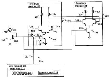
Figure 5 i.s a functional schematic diagram of a line
driver with selectable slew rates and a common idle state
mode of operation according to one embodiment of the
invention. A line driver 180 includes a pre-driver module
182 that is coupled to produce a differential input data
stream to a line driver module 184. Coupled to a
differential input line that carries the input data stream
is a selectable capacitor array 186. Selectable capacitor
2o array 186 provides a plurality of selectable capacitor
configured MOSFETs that may be selectively coupled to the
differential input line to provide a slew rate that
corresponds to a data rate of the input data stream.
Pre-driver module 182 includes a differential pair of
MOSFETs 188 and 190 and a pair of load resistors 192 and
194 coupled between the drains of MOSFETs 188 and 190 and a
supply, respectively. The differential pair of the pre-
driver module 182 are biased by MOSFET 196. MOSFET 196 is
part of a current mirror 198 and is coupled as a mirror
3o device, meaning it conducts a current that is a function of
a reference current! produced by MOSFET 200 that is coupled
as a reference device in the current mirror 198.
More specifically, with respect to the current
produced by the reference device in relation to current
CA 02536641 2006-02-22
WO 2005/027444 PCT/US2004/029863
produced by the mirror device as a function of the
reference current, the amount of current in the two devices
is generally proportional and their magnitudes are a
function of the scaling of the devices in relation to each
other. For two equally scaled devices configured as a
current mirror, the current produced by the mirror device
matches the current produced by the reference device. In
the described embodiment, however, the mirror devices are
scaled to produce approximately five times more current
Zo than the reference device conducts for a similar bias
voltage applied across the gate and source of the device.
Similarly, line driver module 184 comprises a
differential pair of MOSFETs 202 and 204 having drains
coupled to load resistors 206 and 208, respectively, that
1s are further coupled to the supply. The differential pair
of MOSFETs of line driver module 184 are also coupled, at
the source terminals, to MOSFET 210 which is coupled as a
mirror device of current mirror 198. MOSFET 210 also
produces a bias current to the differential pair of MOSFETs
20 202 and 204 that is a function of the reference current
conducted by MOSFET 200 of current mirror 198.
As may further be seen, the amount of current
conducted by MOSFET 200, the reference device of the
current mirror, is set by a current source 212. A drain
25 and a gate of MOSFET 200 are coupled to a gate of MOSFETs
196 and 210 in a typical current mirror configuration.
Thus, if the desired output current level of line driver
module 184 is ten milliamps, and MOSFET 210 is scaled to
conduct five times more current than MOSFET 200 of current
3o mirror 198, the current source 212 should be designed to
provide two milliamps of current because of the relative
scaling of the devices in current mirror 198.
A selectable switch 214 is further coupled to the gate
(input) of MOSFET 196 to selectively provide the bias
16
CA 02536641 2006-02-22
WO 2005/027444 PCT/US2004/029863
signal to MOSFET 196. Accordingly, when the selectable
switch 214 is opened, MOSFET 196 turns off thereby turning
off MOSFETs 188 and 190 of the differential pair of pre
driver module 182. When MOSFETs 188 and 190 are off, the
drains of MOSFETs 188 and 190, which are coupled to the
load resistors 192 and 194, respectively, go to the supply
and produce the supply voltage as an output.
During normal operation, when an input data stream is
being received at the gates of the differential pair of
Zo MOSFETs 188 and 190, pre-driver module 182 produces a
differential input data stream to line driver module 184.
When switch 214 is open and line driver 180 is in an idle
state, pre-driver module 182 produces the supply voltage on
both output lines comprising the differential input of line
driver module 184. Vout is the differential output of line
driver module 184.
As pre-driver module 182 produces the supply voltage
on the differential input line of line driver module 184,
the gates of the differential pair of MOSFETs 202 and 204,
2o which are coupled to the differential input line to receive
either the supply voltage or the input data stream produced
by pre-driver module 182, produce an idle state common mode
output or an output data stream, respectively. If an input
data stream is being received at the gates of MOSFETs 202
and 204, the line driver 184 operates in a normal mode and
produces the output data stream.
Also coupled to the differential input line of line
driver module 184 is a selectable capacitor array 216.
Capacitor array186. Selectable capacitor array 186 216
3o comprises a plurality of selectable capacitors 218 and 220
that may be selectably coupled to the differential input
line to set or adjust a slew rate of the output data stream
produced by line driver module 184. In one embodiment of
17
CA 02536641 2006-02-22
WO 2005/027444 PCT/US2004/029863
the invention, all of the capacitors 218 and 220 of
selectable capacitor array 186 are selectable.
In an alternate embodiment, at least one capacitor 218
(actually a pair of capacitors 218) is permanently coupled
s to each input line of the differential input line to set a
slew rate for the highest data rate of an output data
stream produced by line driver module 184 and is
permanently biased into an operational mode. Capacitors
218 and 220 are scaled differently in the described
io embodiment to provide different amounts of capacitance
according to design requirements. As a slew rate requires
reducing for a slower data rate serial data, selectable
capacitors 220 of varying sues may be added. Such
capacitance values may readily be determined by one of
is average skill in the art.
In the described embodiment, however, all of the
capacitors 218 and 220 are selectable. Further, that only
two capacitors are shown for each differential input shown
by no means limit the number of capacitors of various sizes
ao that can and should be added to produce one of a plurality
of specified slew rates. Accordingly, additional
capacitors 218 are selectively coupled to each line of the
differential input line to adjust the slew rate for slower
data rates for the output data stream.
25 As is known by one of average skill in the art, one
may merely add a capacitance of capacitors coupled in.
parallel, thus facilitating the addition of additional
capacitors of the selectable capacitor array to adjust the
slew rate. As capacitance increases, a total charge time
so increases thereby increasing the rise time of the bits of
the input data stream (the slew rate of the input data
stream) .
In the described embodiment of the invention, the
capacitors 218 are actually capacitor configured MOSFETs
18
CA 02536641 2006-02-22
WO 2005/027444 PCT/US2004/029863
218 and 220 coupled to each differential input line of the
line driver module 184. Accordingly, a bias signal
received by each MOSFET 218 or 220 biases the capacitor
configured MOSFETs 218 and 220 into an operational state.
In one embodiment the other end of the capacitors 218 and
220 are coupled to the slew rate logic 226, where the slew
rate logic 226, includes circuitry comprising the slew rate
setting 164 signal connected to two inverters in series
which in turn are connected to the other end of the
so capacitors 218 and 220 (or in another embodiment the slew
rate setting 164 signal is connected directly to the other
end. of the capacitors 218 and 220, i.e., the slew rate
setting 164 signal is the bias signal). In place of
capacitor configured MOSFETs, however, one may include
actual capacitors that are switched in and out of coupling
with. a selectable switch, where, in one embodiment, one end
of the selectable switch is connected to ground and the
other end to the capacitor and the control to the switch is
provided by the slew rate logic 226, which is directly or
2o indirectly connected to the slew rate setting 164.Line
driver 180 further includes slew rate and idle state logic
222. Slew rate and idle state logic 222 further includes
slew rate logic block 226 and idle state logic block 224.
Idle state logic block 224 produces an idle signal to open
switch 214 to remove a bias signal from MOSFET 196 of
current mirror 198. Accordingly, when idle state logic
block 224 produces the idle signal, a bias signal is
removed from MOSFETs 188 and 190 of the differential pair
of pre-driver module 182 to turn off MOSFETs 188 and 190 to
3o cause pre-driver module 182 to output the supply voltage as
has been described above. The logic of idle state logic
block 224 and slew rate logic block 226 may be formed in
programmable logic fabric 12 of Figure 1 or in control
modules 30 and 35, among other places according to design
19
CA 02536641 2006-02-22
WO 2005/027444 PCT/US2004/029863
preferences. As may also be seen, a switch 215 is provided
to ground the gate of MOSFET 196 whenever switch 214 is
opened to remove the bias signal from MOSFET 196 in order
to ensure that the MOSFET is biased into a non-operational
mode. In one embodiment the idle logic block 224 includes
circuitry comprising two series connected inverters
connected to the idle state setting 165. The output of the
first inverter is the idle bar (complement of idle) signal
and the output of the second inverter is the idle signal
to (FIG. 6) .
Slew rate logic block 226 is coupled to receive a data
rate indication and produces corresponding bias signals to
MOSFETs 218 or 220 to selectively couple (biasing to an on
state) 218 or 220 to each line of the differential input
line to adjust the slew rate to a value that corresponds
with the received data rate. For example, if line driver
180 supports only two data rates, then slew rate logic
block 226 selects one of two combinations of capacitors to
establish one of two corresponding slew rates. In one
2o embodiment of the invention, four different slew rates are
selectable and are provided for. It is understood that the
number of actual selectable slew rates is a matter of
choice for one practicing the invention.
To clarify operation of the present invention, Figures
6 and 7 are functional schematic diagrams that illustrate
the various modes of operation of line driver 180.
Referring now to Figure 6, the idle state mode of operation
is illustrated. As may be seen, selectable capacitor array
186 is not shown in Figure 6. Moreover, the corresponding
3o slew rate logic block 226 is shown in dashed lines. ~nlhile
the line driver 180 is in an operational mode, the idle
state logic block 224 does not assert the idle signal to
cause switch 214 to remain closed and switch 215 to remain
open. The operational mode idle signal produced by idle
CA 02536641 2006-02-22
WO 2005/027444 PCT/US2004/029863
state logic block 224 is shown in Figure 6. When idle
state logic block 224 asserts the idle signal during an
idle mode, however, switch 214 opens to remove a bias
signal from MOSFET 196 of current mirror 198. Similarly,
s switch 215 closes to ground the gate of MOSFET 196.
Because this results in MOSFETs 196, 188 and 190 being
turned off, MOSFETs 196, 188 and 190 are shown in dashed
lines. As the impedance of a gate terminal, and more
specifically, the gates of MOSFETs 202 and 204 approach
Zo infinity, the output nodes of pre-driver module 182
approach the supply voltage because no current is conducted
through the load resistors 192 and 194. Accordingly, the
output voltage of Vsupply is produced from pre-driver module
182.
15 As is known by one of average skill in the art, only
one of the differential MOSFETs will be on at a time and
producing an output during an operational mode.
Accordingly, the output signal magnitude is a function of
the bias current produced by MOSFET 210 of current mirror
20 198 and a value of the load resistors 206 and 208. When
both MOSFETs 202 and 204 are on during idle state mode of
operation because both gates are receiving the supply
voltage produced by pre-driver module 182, however, the
current in each differential MOSFET 202 and 204 is one half
25 of the current in MOSFET 210. Accordingly, a differential
output produced at the drains of MOSFETs 202 and 204 has
one half of the signal magnitude of an output signal
produced during normal operation.
Referring now to Figure 7, the idle state logic block
30 224, the line that carries the idle signal, as well as
switch 214 are all shown in dashed lines to indicate that
they need not be electrically present for the purpose of
this discussion. The operation of slew rate logic block
226 is as described. Slew rate logic block 226 produces
21
CA 02536641 2006-02-22
WO 2005/027444 PCT/US2004/029863
bias signals to capacitor configured MOSFETs 218 and 220 to
selectively couple the capacitor configured MOSFETs 218 and
220 to provide a slew rate that corresponds with a serial
data rate.
Figure 8 is an example of a signal diagram showing a
logic one signal transmitted at two different rates and the
corresponding slew rates. This example is for illustration
purposes only. For example, signal "a" might be a 10
Gigabit input data stream signal while signal "b°' might be
so a 1 Gigabit output data stream signal. The rise timeof
signal "a" is shown as "ta" while the rise time of signal b
is shown as "tb°'. The slew rate corresponds to these shown
rise times. Thus, by adding capacitance to the input data
stream, the rise time transitions from to to tb thereby
decreasing the slew rate.
Figure 9 is a flow chart illustrating operation of the
present invention according to one embodiment of the
present invention. Initially, the inventive method
includes determining whether the Tx line driver, for
2o example, line driver 180, is in one of an idle state or in
an operational state (step 230). If the Tx line driver is
in an idle state, steps 232 through 240 are performed. If
the Tx line, driver is in an operational state, then steps
242 though 248 are performed.
2s If the Tx line driver is in an idle state, the next
step of the invention includes producing an idle state mode
signal to a switch and removing a bias signal from a pre-
driver module (step 232). In one embodiment of the
invention, a switch configured MOSFET is coupled in series
3o with a gate of a MOSFET that provides a bias signal to a
differential pair of the pre-driver module. Thus, to open
the circuit and remove the bias signal, the idle state mode
signal is one that turns off the switch configured MOSFET
to open a connection between a bias signal and the gate of
22
CA 02536641 2006-02-22
WO 2005/027444 PCT/US2004/029863
the MOSFET that provides the bias signal to differential
pair of the pre-driver module.
Thereafter, the method includes turning off a
differential pair of the pre-driver module (step 234) and
producing an output from the pre-driver module that is
equal to a supply voltage (step 236). Because the bias
signal to the differential pair is removed, the MOSFETs of
the differential pair are turned off causing a differential
output of the pre-driver module to go to the supply
to voltage.
As the output of the pre-driver module goes to the
supply voltage, both MOSFETS of a differential pair of a
line driver module are biased into an on state. Because
the current level through a biasing MOSFET is fixed by a
i5 current mirror configuration, the total bias current is
divided through each MOSFET of the differential pair of the
line driver module. Thus, the method includes conducting
equal amounts of current through the differential pair of
the line driver module (step 238). This equal amount of
2o current is one half of a signal magnitude during normal
operation. Accordingly, the voltage drop across a pair of
load resistors coupled to the drains of the differential
pair of the line driver module is one half, thereby
producing a common mode idle state output from the Tx line
2s driver (step 240) .
If the Tx Line driver is in an operational state, the
method includes determining a data rate for an outgoing
data stream (step 242). In one embodiment of the
invention, the data rate is received from external logic.
3o Based upon the received data rate during normal operation,
the invention further includes determining what capacitors
should be coupled to produce a corresponding slew rate
(step 244) and producing corresponding bias signals to
selectively couple selected capacitors (step 246). Thus,
23
CA 02536641 2006-02-22
WO 2005/027444 PCT/US2004/029863
the invention includes coupling selected capacitors to a
differential input data stream and producing a
corresponding slew rate for the outgoing data stream (step
248) .
s The invention disclosed herein is susceptible to
various modifications and alternative forms. Specific
embodiments therefore have been shown by way of example in
the drawings and detailed description. It should be
understood, however, that the drawings and detailed
so description thereto are not intended to limit the invention
to the particular form disclosed, but on the contrary, the
invention is to cover all modifications, equivalents and
alternatives falling within the spirit and scope of the
present invention as defined by the claims.
24