Note: Descriptions are shown in the official language in which they were submitted.
CA 02536724 2006-02-16
Title
AMORPHOUS SELENIUM FLAT PANEL X-RAY IMAGER FOR
TOMOSYNTHESIS AND STATIC IMAGING
Field
This patent specification is in the field of radiography and pertains more
specifically
to x-ray imaging using a digital, flat panel x-ray imager.
Background
Flat panel x-ray imaging devices that use charge generator materials such as
doped
amorphous selenium charge generator layers and directly convert x-rays to
electrical
charges and thus generate electrical signal related to local x-ray exposure,
have been
developed in recent years. See, for example U.S. Patent No. 5,319,206, and
Yorker J.,
Jeromin L., Lee D., Palecki E., Golden K., and Jing Z., "Charactrerization of
a full field
mammography detector based on direct x-ray conversion in selenium," Proc. SPIE
4682,
21-29 (2002). Commercial versions for general radiography and for mammography
have
been available for more than a year in this country from Hologic, Inc. of
Bedford, MA
("Hologic") and Direct Radiography Corporation of Newark, DE. ("DRC"). The DRC
imager is used in mammography systems that have been available for more than a
year in
this country from Lorad Corporation of Danbury, CT ("Lorad"). In such direct
conversion panels , the charge generator material directly converts x-ray
photons into
electron-hole pairs and, under an applied electrical field, the holes and
electrons barrier to
respective electrodes with very little lateral loss to neighboring pixels.
Direct conversion
is believed to offer better,spatial resolution and other advantages over
indirect conversion
panels, in which x-ray photons cause scintillation in a material such as
cesium iodide and
the resulting light energy in detected.
The structure of a direct conversion flat panel imager of the type referred to
above is
illustrated in principle but not to scale in Fig. 5. It comprises a top
electrode 500, a
charge barrier layer 502 (typically made of Parylene) separating the top
electrode from an
CA 02536724 2006-02-16
amorphous selenium-based charge generator layer 504, an electron blocking
layer 506
patterned into a two-dimensional pixel array, a charge collection electrode
508 that also is
patterned into a pixel array, a TFT array comprising respective transistors
510 coupled to
the charge collection electrode and to respective signal storage capacitors
512, a substrate
514 typically made of glass, a gate pulse line 516 that enables (turns ON) the
transistors
to deliver to charge amplifiers 518 the charges collected at the respective
storage
capacitors, an a programmable high voltage power supply 520. The illustrated
equivalent
capacitor circuit for a pixel comprises a capacitor 522 representing
capacitance across the
charge barrier layer, a capacitor 524 representing capacitance across the
charge generator
layer, and a capacitor 526 representing capacitance of the charge storage
capacitor far the
pixel. One of the functions of the charge barner layer is protection of the
thin-film
transistors, which can suffer breakdown damage if the charge stored in the
charge storage
capacitors becomes too high, e.g. when a capacitor stores charges generated at
a region of
the charge generating layer that receives x-rays that have not been attenuated
by the
object being imaged. For example, in mammography the corners of the flat panel
imager
typically are outside the breast outline and receive much more radiation than
the part of
the imager under the breast. The charge barrier layer protects such
transistors by
collecting charges that gradually reduce the electrical field in the
appropriate portions of
the charge generator layer, and thus reduce the amount of charge that would
otherwise
collect at the pertinent charge collection capacitors.
The charge barrier layer thus contributes to meeting one of the challenges in
flat panel
detectors, namely, breakdown protection of the thin-film transistors. Another
challenge
is ghosting (remnants of one or more previous images) due to the time it takes
to dissipate
charges collected in the imager from previous x-ray exposures. Various
techniques have
been developed and used commercially to remove or at least reduce ghosting to
an
acceptable level. They include charge erasing by exposure to visible light
between x-ray
exposures and various ways to manipulate the bias potential of electrodes
between x-ray
exposures. The time needed to attend to ghosting makes it difficult to take
images in
rapid succession, such as for fluoroscopy or tomosynthesis
It has been reported that it would be impractical to use a direct conversion
panel
without a charge barrier layer. Thus, a 1998 paper by well-known researchers
in direct
2
CA 02536724 2006-02-16
conversion panels states that direct metallization of a selenium based
detector in theory
would allow for rapid imaging but concluding based on experimental data that
this gives
non-reproducible and unstable results. Polischuk B, Shukri Z., Legros A. and
Rougheout
H., "Selenium direct converter structure for static and dynamic x-ray
detection in medical
imaging applications," SPIE Conference on Physics of Medical Imaging, San
Diego, CA,
February 1998, SPIE Vol. 3336, pp. 494-504, states that "In order to develop a
selenium
based x-ray detector which could operate in real time, i.e. 30 frames per
second, a direct
metallized selenium structure would be required. It is well established in
solid-state
theory that metallic electrodes deposited directly onto the free surface of
semiconductor
layers can behave as Schottky contacts." The paper states then states that
"most metals
with lower work functions [than selenium] should have built-in potential
barriers which .
could minimize the injection of excess charge from the metal electrode," but
reports that
tests showed that "sample-to-sample variability and contact instability were
common
observations on these samples," and that: "It was therefore concluded that any
x-ray
detector which relied only on the Schottky contact to limit dark currents
would provide
non-reproducible and unstable results." The paper proposes the solution of
including a
blocking layer between the top electrode and the selenium, and states that
"The role of
the top blocking layer is to limit the injection of positive charge from the
metallic
electrode, but allow any x-ray-generated electron to move unimpeded from the
selenium
layer to the metallic contact." The authors of the article are from Noranda
Advanced
Materials of Quebec, Canada, an entity that is believed to have been a major
developer at
the time of flat panel selenium-based x-ray imagers, in addition to DRC.
A number of earlier proposals have dealt with the issue of high voltage
protection in
flat panel detectors. U.S. Patent No. 6,353,229, granted to the three authors
of the 1998
paper and two other inventors, refers to several such proposals. One is cited
at column 1,
lines 24-39 and is reported to involve a special dual-gate TFT (thin-film
transistor)
structure that forms a back channel in the TFT structure if the pixel voltage
exceeds a
certain potential. See, Zhao W., Law J., Waechner D., Huang Z., and Rowlands
J.,
"Digital radiology using active matrix readout of amorphous selenium detectors
with
high voltage protection," 1998 Med Phys 25 (4), pp. 539-549. Another is
discussed at
column 1, lines 46-57 U.S. Patent 5,198,673) and is said to involve the use of
a second
3
CA 02536724 2006-02-16
two-terminal protection device resident at each pixel location. The patent
also refers, in
the section entitled "Description of Prior Art," to a number of other items of
prior art: ( 1 )
PCT International Application WO 96/22616 published Jul 25, 1996; (2) Lee D.,
Cheung
L.K., and Jeromin L., "A new digital detector for projection radiography,"
1995, SPIE
Vol. 2432, pp. 237-249; (3) U.S. Patents No. 5,598,004 and 5,396,072 (stating
that "no
mention is made [in those patents] of the high voltage protection of the TFT
array"); (4)
U.S. Patent No. 5,528,043 (stating that the patent "does not mention whether
high voltage
protection of the circuit from the selenium bias is achieved"); (5) U.S.
Patent No.
5,436,101 (stating that "there is no mention of any high voltage protection of
any element
on the substrate"); and (6) Canadian patent application 2,184,667 published
March 4,
1998 and corresponding EP 0 826 983 published the same day (stating that "no
indication
of how this structure could be used for high voltage protection is given").
U.S. Patent No. 6,353,229 proposes to achieve high voltage protection "by
setting the
high voltage biasing electrode to a negative potential and the TFT "off ' gate
voltage to a
predetermined negative value such that the TFT is essentially non-conductive."
The
patent recognizes that "there will always be some TFT leakage" but states that
"the
negative "off ' voltage may be adjusted so as to minimize the same and render
the TFT
essentially non-conductive." See column 2, lines 49-61.
Earlier papers and patents are believed to be consistent with the patents and
papers
cited above. See U.S. Patents Nos. 5,132,541, 5,184,018, 5,396,072, and
5,942,756, and
Zhao W. and Rowlands J.A., "A large area solid-state detector for radiology
using
amorphous selenium," SPIE Medical Imaging, Vol. 1. 1651, pp. 134-143, 1992.
Each of the patents and papers cited above is hereby incorporated by reference
in this
patent specification as though fully set forth herein.
Summary of Disclosure
This patent specification discloses a new approach that departs from, and in
some
ways contradicts, the proposals in the patents and papers cited above. The new
approach
includes placing a top electrode directly on and in physical and electrical
contact with a
selenium-based charge generator layer, and intentionally uses leakage current
of the TFT
array transistors for protection. In the new approach, the leakage current
characteristics
4
CA 02536724 2006-02-16
of the TFT array transistors provide an operating regime in which the leakage
current is
relatively low for pixels that measure radiation within the typical range
expected for the
object being imaged but the leakage current is sufficiently high to avoid
transistor
breakdown for pixels that receive more radiation, e.g. pixels that are outside
the object
being imaged and receive radiation that is not attenuated by the object, such
as pixels at
corners of the imager. In the new approach, the TFT leakage current regime
provides
breakdown protection despite the absence of a charge barrier layer between the
top
electrode and the charge generator layer designed to protect from high voltage
TFT
breakdown.
In a preferred but non-limiting example, a top metal electrode is deposited or
otherwise formed directly on the selenium-based layer, with no deliberately
formed
charge blocking or insulating layer between the top electrode and the charge
generator
layer. The leakage current of the thin-film transistors rises at a relatively
low rate with
voltage at the transistors up to a selected range but rises much more steeply
with voltage
at the transistors above that range. As a non-limiting example for a specific
circuit
configuration, the leakage current rises at a low rate up to transistor
voltage in the range
of 20-25 volts but rises much more steeply with voltage above that range. At
higher
voltage, the steeply rising leakage current provides built-in protection
against transistor
breakdown. The range of 20-25 volts is only an example, and other ranges may
be
appropriate to accomplish protection in the case of differently structured TFT
array
transistors or imagers.
Brief Description of the Drawing
Fig. 1 illustrates a partial cross-section of an x-ray imager panel
incorporating an
example of the technology disclosed in this patent specification.
Fig. 2 is a partly block-diagram and partly circuit diagram of a portion of
the imager
of Fig. 1.
Fig. 3 illustrates voltage vs. leakage current characteristic of a thin-film
transistor
used in Fig. 2.
CA 02536724 2006-02-16
Fig. 4 illustrates a comparison of ghosting characteristics of an imager using
the
disclosure of this patent specification and a prior art imager.
Fig. 5 illustrates a prior art x-ray imager panel in a view similar to that of
Fig. 1.
Figs. 6a and 6b show graphs illustrating linearity of an imager according to
Figs. 1-3
in screening mode and in tomosynthesis mode, respectively.
Figs. 7a and 7b show graphs illustrating modulation transfer function (MTF) of
an
imager according to Figs. 1-3 in screening mode and in tomosynthesis mode,
respectively.
Fig. 8 shows a graph illustrating noise power spectrum (NTS) of an imager
according
to Figs. 1-3 in screening mode.
Figs. 9a-9b and Fif. 9c show graphs illustrating detector quantum efficiency
(DQE) of
an imager according to Figs. 1-3 in screening mode and in tomosynthesis mode,
respectively.
Fig 10 shows a graph illustrating ghost(%) characteristics of an imager
according to
Figs. 1-3 in screening mode.
Fig. 11 shows a graph illustrating image lag as a function of elapsed time of
an
imager according to Figs. 1-3 in tomosynthesis mode.
Fig. 12 shows a graph illustrating residual image ghost as a function of time
of an
imager according to Figs. 1-3 in tomosynthesis mode.
Detailed Description of Preferred Embodiments
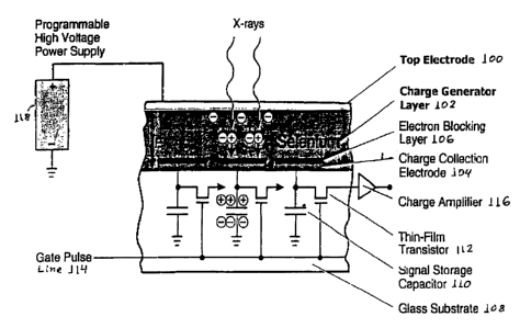
Referring to Fig. 1, a non-limiting example of an imager incorporating the
teachings
of this patent specification comprises a top electrode 100 deposited or
otherwise formed
directly on, and in physical and electrical contact with, an upper surface of
an amorphous
selenium-based charge generator layer 102. Unlike the case illustrated in Fig.
5, there is
no deliberately deposited or otherwise formed charge barrier layer, although
it is possible
that some unappreciated interaction may take place at the interface between
top electrode
100 and charge generator layer 102 exhibiting some barrier effects. A charge
collection
electrode 104 is patterned into a two-dimensional array of pixel electrodes
that are under
charge generator layer 102 or are embedded at a bottom surfaces thereof. An
electron
6
CA 02536724 2006-02-16
blocking layer 106 may cover pixel electrodes 104 (also called charge
collection
electrode). A read-our circuit is interposed between charge generator layer
102 and a
substrate 108, and comprises respective signal storage capacitors 110 coupled
electrically
with the pixel electrodes and a thin-film transistor (TFT) array comprising
respective
gating transistors 112 coupled electrically with the junctions between the
pixel electrodes
and the signal storage capacitors. Transistors 112 are normally in an OFF
state but can
be enabled (turned ON) by a gating signal delivered over gate pulse line 114,
to thereby
deliver charge accumulated in signal storage capacitors to a charge amplifier
116. A
programmable high voltage power supply 118 applies a positive potential to top
electrode
100 relative to ground and to grounded signal storage capacitors 110, to
thereby induce
an electrical field in charge generator layer 102. Additional electrical
fields can be
generated as well, for example by forming and appropriately biasing special
electrodes
that extend into the underside of charge generator layer 106, between adjacent
charger
collector electrodes 104. Fig. 1 is not to scale, and omits well known
components of an
imaging panel, such as a protective layer over top electrode 100 (e.g.
Parylene
passivation over an A1 top electrode, or any protective layer over the top
electrode) and
various other mechanical or electrical components that are a part of the
imaging panel
that has been available from DRC and used by Lorad for mammography and has
3584 by
4096 square pixels of 70 microns each over an active area of about 25 by 29
cm. The
charge generator layer is about 200 microns thick and is thermally stabilized
by
controlled amounts of dopants. A voltage of about 1,000 volts across the
charge
generator layer can be used, resulting in an electric field of about 5 volts
per micron
thickness.
Referring to Fig. 2, the components that are the same as in Fig. 1 bear the
same
reference numerals. The additional components are: additional gate pulse lines
GZ ... Gn
that are similar to line 114 (G,) but serve other rows of transistors 112, a
gate driver 200
directed by a controller 202 to selectively enable transistors 112 in the
respective rows,
and column readout lines Di ... Dm that feed the outputs of transistors 112 in
respective
columns to sample-and-hold (S/H)circuits 204. A multiplexer 206 takes the
output of
circuits 204 and feeds analog-to-digital converters (ADC) 210, also controlled
by
controller 202. Digitized pixel values from ADC 208 are delivered to serial
data port 210
7
CA 02536724 2006-02-16
and then to an image buffer, from which they can be taken for appropriate
processing into
image data for display, storage, transmission, etc. The pixel charges can be
read out
individually, or several pixels (e.g. an array of 2 by 2 pixels) can be binned
into a single
sample for higher reading speed at the expense of spatial resolution. The
panel can be
operated in a static mode for screening mammography, for example at a 28 kVp,
MO/MO
spectrum provided by an x-ray generator from Lorad designated M4, with an
image cycle
of 30 seconds and at a source-detector distance of 65 cm. For test purposes,
an exposure
range of 1 to 16 mR can be used, which subsumes the typical dose of 1-10 mR
for breast
cancer screening. Alternatively, the panel can be operated in a dynamic,
tomosynthesis
mode, for example using a 28 kVp, Mo/Rh spectrum, with an image cycle of 0.5
or 1.0
seconds and 2x2 pixel binning, and at exposure range of 0.5-1.5 mR per image,
i.e. at a
dose range per image of about a factor of 10 less than for the static,
screening mode so
that about 10 images can be taken in dynamic, tomosynthesis mode in one sweep
of stop-
and-expose imaging.
Fig. 3 illustrates leakage current characteristics of a thin-film transistor
112 that are
particularly important for the operation of the imager of Figs. 1 and 2. As
seen, when the
transistor is in its OF'F state, and the voltage at the transistor drain 112a
(at the junction
between the respective signal storage capacitor 110 and pixel electrode 104)
is less than
about 20 volts, or at least less than somewhere in the range of about 20-25
volts, the
leakage current of the transistor rises at a relatively low rate. However,
with the
transistor still in its OF'F state, the leakage current rises at a
significantly higher rate
(more steeply) with rise in the voltage at 112a above the range of about 20-25
volts. In
the example, the inflection point between low and high rates of leakage
current rise is
closer to 20 volts than to 25 volts. In this example, the rise above the
inflection point is
progressively steeper. While the exact point of inflection or range in which
the point of
inflection occurs may vary depending on the details of a particular TF'T
array, the
important feature is that the leakage increase at a sufficiently high rate
above a voltage
range appropriate for a particular use of an imager panel to avoid voltage
breakdown of
(or overvoltage damage to) the transistors.
As illustrated in Fig. 4, one of the benefits of an x-ray imager of the type
illustrated in
Figs. 1-3 is a dramatic decrease in ghosting effects as compared with a prior
art imager of
8
CA 02536724 2006-02-16
the type illustrated in Fig. 5. Fig. 3 compares ghosting of an imaging panel
currently sold
by Direct Radiography Corporation (standard DRC detector) with an otherwise
similar
panel of the type illustrated in Figs. 1-3 (metal on selenium detector): A
significant
difference between the two detectors (x-ray imaging panels) is that the
standard DRC
detector has a charge barrier layer (layer 502 in Fig. 5) while in the metal
on selenium
detector the top electrode 100 is directly on the charge generator layer 102
as seen in Fig.
1. Indeed, the two panels can be otherwise identical, with identical TFT
arrays.
However, transistors 112 in the metal on selenium detector of Fig. 1 operate
in a different
regime, in which they are allowed to extend the voltage at drain 112a into a
range that the
charge barner layer 502 in the standard DRC detector was designed to prevent.
The low ghosting that the metal on selenium detector exhibits (the x-ray
imager of
Figs. 1-3) allows for rapid imaging as compared with the standard DRC
detector. While
the x-ray imager of Figs. 1-3 may use technology for erasing ghost images
between x-ray
exposure that is the same or similar to those used in the imagers currently
sold by Direct
Radiology Corporation, in the alternative it may be possible to use the imager
of Figs. 1-3
without such erasing.
The top electrode 100 typically is elemental metal or an alloy or inorganic
oxide such
as Indium-Tin Oxide (ITO), but an organic conductor may be used instead. The
material
of top electrode 100 preferably has a lower work function than the underlying
charge
generator layer. Preferably, top electrode 100 is made of a material that
would allow a
free flow of negative charge from the charge generator layer 102 into
electrode 100 while
inhibiting the injection of positive charge from electrode 100 into charge
generating layer
102. Preferably, but not necessarily, the material of top electrode 100 has
the following
characteristics: work function < 4.0 electron volt; electrical resistivity <
55 u.ohm.cm;
atomic number < 60. Further, the material of top electrode 100 preferably is
chemically
stable when in contact with selenium, is not flammable in solid form and is
neither
explosive nor corrosive, is not too toxic or carcinogenic or radioactive, and
allows the
formation of top electrode 100 by a deposition or other process compatible
with forming
the remaining structure of the imaging panel. Chromium (Cr) is believed to be
an
example of a suitable material that meets the criteria set forth above, for
example in
thickness of 1,000 Angstroms, although other thicknesses also may be suitable.
ITO and
9
CA 02536724 2006-02-16
A1 in elemental form or as the predominant metal in an alloy with each other
or with
other elements, also are believed to be examples of suitable materials. The
chemical
stability Al, In, and Ti in elemental form or in alloys with each other or
other metals, with
selenium in the panel of Figs. 1-3 may need to be confirmed. Cs meets the
other
requirements, but its chemical stability with selenium may present challenges.
Ba, Tb,
and Be also may work if safety/health issues that they pause are overcome.
Another
consideration is thermal expansion compatibility with selenium, which may
impose
conditions on the composition of thickness of the top electrode.
The ability to rely on transistor leakage current to avoid breakdown under the
expected operating conditions an x-ray imaging panel may be surprising given
common
assumptions in x-ray imaging technology. For example, in mammography uses of
the
prior art panel illustrated in Fig. 5 that had been commercially available, it
had been
believed that without charge barrier layer 502 such a high amount of charge
would
accumulate at the individual signal storage capacitors 512 that the capacitor
voltage
would rise to a level sufficiently high to damage the dielectric in the
capacitor and/or the
channel in the thin film transistor 510, leading to permanent damage of the
imaging
panel. One calculation assumes that the leakage current is zero, and estimates
that under
mammography x-ray energies the imaging panel is accumulating 4.58x10-'5
Coulomb per
mR per pixel.. If the maximum x-ray exposure rate is 5R/secorid, then the
maximum
accumulated charge at capacitor 512 is 2.3x10-" Coulomb in 1 second. This
theoretical
calculation leads to a voltage of 34.7 volts across signal storage capacitor
512. In
practice, in the case of a large and dense breast, the exposure rate is closer
to 3 R/second.
While this is the estimate assuming there is no leakage current, actual
measurements of
the TFT in the current mammography imaging panels (Fig. 5) supplied by DRC
indicate
a rapidly increasing drain-to-source leakage current with increasing voltage
over about
20-25 volts. At about 30 volts at the drain, the leakage current is
interpolated to be 24
pA, just enough to leak away excess charge as the signal storage capacitor
potential roses
over 25 volts. This rapidly rising leakage current thus becomes a self-
protecting
mechanism, which in turn allows dispensing with a charge barrier layer such as
502 (Fig.
5) and its ghosting effects.
CA 02536724 2006-02-16
Tests in the screening mode of a mammography panel according to Figs. 1-3, at
the
parameters set forth above, suggest:
~ Good linearity at the expected exposure range (see Fig. 6a);
~ Good presampling modulation transfer function (MTF) (see Fig. 7a);
~ Good noise power spectrum (NPS) as a function of spatial frequency for
different exposure over the expected range (see Fig. 8);
~ Good efficiency expressed as detective quantum efficiency (DQE) as a
~ composite parameter that measures the efficiency of an imaging system in
transferring the input signal to noise ratio at the output according to the
expression
DQE (f,X) _ (S(X)xMTF(f))2 /(~(X)xNPS(f,X))
where S(X) is the measured signal at a certain exposure X, ~(X) is the
incident photon fluence per unit area at exposure X (see Figs 9a-9b); and
~ Good ghosting characteristics as a function of elapsed time (see Fig 10) in
a
test where the imager was exposed to a large "ghost" exposure of 2.6 R with a
28 kVp, Mo/Mo spectrum, with part of the imaging surface being covered by
a piece of 1.0 mm thick sheet of lead. 30 seconds later, the first read frame
was acquired at a much lower dose of 9 mR, with the lead removed and the x-
ray beam filtered through 4 cm of Lucite. The mean detector signals in a 256
by 256 pixel region of interest inside and outside the Lucite phantom location
were compared, and ghosting magnitude was calculated as the normalized
difference:
Ghost(%) _ ((signal(inside) - signal(outside))/signal(inside)x100%.
Tests in the tomosynthesis mode of a mammography panel according to Figs. 1-3,
at
the parameters set forth above, also suggest:
~ Good linearity at the expected exposure range (see Fig. 6b);
~ Good presampling modulation transfer function (MTF) (see Fig. 7b);
~ Good efficiency (Fig. 9c) expressed as detective quantum efficiency (DQE)
calculated using the methodology used in the screening mode but at the
tomosynthesis parameters;
11
CA 02536724 2006-02-16
~ Good image lag characteristics (Fig. 11 ), where lag was investigated by
exposing the imager to a single high exposure at 28 kVp with half the imaging
area covered by a 1.0 mm thick sheet of lead, then reading out a series of
dark
image frames at 0.5 second intervals. Two tests were done, one with a high
dose of 164 mR, the other with 58 mR. Lag was calculated as the normalized
difference in the dark counts between the unshielded area exposed to the high
dose and the other half that was shielded by the lead:
Lag(%) _ ((dark counts(unshielded) - dark counts(shielded))/dark counts
(shielded)x 100%; and
Good residual image ghost as a function of time (Fig. 12), investigated by
exposing the imager to a high ghost exposure of 177 mR with a 36 kVp Mo/Rh
spectrum, with a part of the imager covered with a 4.2 cm thick acylic block.
A
series of read dose images then followed at 1.0 second intervals, with the
acrylic
block removed and at 5.29 mR for each image frame.
The graphs discussed above are for a specific configuration of an example of a
panel,
and it should be clear that different results may be obtained with different
embodiments
of the invention set forth in the appended claims or with different test
conditions.
It should be understood that the disclosure above illustrates only non-
limiting
examples of the claimed inventions, that variations will occur to those
skilled in the
pertinent technologies, and that the scope of the inventions recited in the
appended claims
is not limited to those examples.
12