Note: Descriptions are shown in the official language in which they were submitted.
CA 02537476 2006-03-O1
WO 2005/024951 PCT/CA2004/001592
SPHERE-SUPPORTED THIN FILM PHOSPHOR
ELECTROLUMINESCENT DEVICES
CROSS REFERENCE TO RELATED U.S. PATENT APPLICATION
This patent application claims the priority benefit from United States
Provisional Patent Application Serial No. 601500,375 filed on September 5,
2003 entitled SPHERE-SUPPORTED THIN FILM PHOSPHOR
ELECTROLUMINESCENT DEVICES, and which is incorporated herein in
its entirety.
FIELD OF THE INVENTION
The present invention relates to materials and structures for thin
film electroluminescent devices, and more particularly the present
invention relates to sphere-supported thin film phosphor
electroluminescent (SSTFEL) devices.
BACKGROUND OF THE INVENTION
Thin film electroluminescent (TFEL) devices typically consist of a
laminar stack of thin films deposited on an insulating substrate. The thin
films include a transparent electrode layer and an electroluminescent (EL)
layer structure, comprising an EL phosphor material sandwiched between
a pair of insulating layers. A second electrode layer completes the
laminate structure. In matrix addressed TFEL panels the front and rear
electrodes form orthogonal arrays of rows and columns to which voltages
CA 02537476 2006-03-O1
WO 2005/024951 PCT/CA2004/001592
are applied by electronic drivers, and light is emitted by the EL phosphor
in the overlap area between the rows and columns when sufficient voltage
is applied in excess of a voltage threshold.
TFEL devices have the advantages of long life (50,000 hours or
more to half brightness), wide operating temperature range, high contrast,
wide viewing angle and high brightness.
In designing an EL device, a number of different requirements have
to be satisfied by the substrates, the laminate layers and the interfaces
between these layers. To enhance electroluminescent performance, the
dielectric constants of the insulator layers should be high. To work reliably
however, self-healing operation is desired, in which electric breakdown is
limited to a small localized area of the EL device: The electrode material .
covering the dielectric layer fails at the local area, preventing further
breakdown. Only certain dielectric and electrode combinations have this
self healing characteristic. At the interface between the phosphor and
insulator layers, compatibility between materials is required to promote
charge injection and charge trapping, and to prevent the interdiffusion of
atomic species under the influence of the high electric fields during
operation, and also at the temperatures required to fabricate the EL
device.
Standard EL thin film insulators, such as SiO~, Si3N4, AI203, SiOXNy,
SiAIOXNy and Ta205 typically have relative dielectric constants (K) in the
2
CA 02537476 2006-03-O1
WO 2005/024951 PCT/CA2004/001592
range of 3 to 60 which we shall refer to as low K dielectrics. These
dielectrics do not always provide optimum EL performance due to their
relatively low dielectric constants. A second class of dielectrics, called
high
K dielectrics, offer higher performance. This class includes materials such
as SrTi03, BaTi03, PbTi03 which have relative dielectric constants
generally in the range of 100 to 20,000, and are crystalline with the
perovskite structure. While all of these dielectrics exhibit a sufficiently
high
figure of merit (defined as the product of the breakdown electric field and
the relative dielectric constant) to function in the presence of high electric
fields, not all of these materials offer sufficient chemical stability and
compatibility in the presence of high processing temperatures that may be
required to fabricate an EL device. Also, it is difficult to form high
dielectric
constant insulating layers as thin films with good breakdown protection.
Substrates are also of fundamental importance for TFEL devices.
Glass substrates are in commercial production. At temperatures
significantly higher than 500°C, glass softens and mechanical
deformation
may occur due to stresses within the glass. For this reason, the maximum
processing temperature of TFEL phosphors is of great significance.
Yellow-emitting ZnS:Mn TFEL displays are compatible with glass
substrates, however, many TFEL phosphors require higher processing
temperatures. Example include blue emitting BaA12S4:Eu, which is typically
annealed at 750°C (Noboru Miura, Mitsuhiro Kawanishi, Hironaga
3
CA 02537476 2006-03-O1
WO 2005/024951 PCT/CA2004/001592
Matsumoto and Ryotaro Nakano, Jpn. J. Appl. Phys., Vo1.38 (1999) pp.
L1291-L1292), and green-emitting Zn2Sio.5Geo.504:Mn, which is annealed
at 700°C or more (A.H.Kitai, Y. Zhang, D. Ho, D. V. Stevanovic, Z.
Huang,
A. Nakua, Oxide Phosphor Green EL Devices on Glass Substrates, SID
99 Digest, p596-599 ).
Substrates other than glass may be used, and Wu in United States
Patent No. 5,432,015 teaches the application of ceramic substrates such
as alumina sheets for TFEL devices. In such devices, thick film, high
dielectric constant dielectrics are prepared. These dielectrics are in the
range of 20 p,m thick and are deposited by a combination of screen
printing and sol-gel methods onto metallized alumina substrates, and are
generally based on lead-containing materials such as PbTi03 and related
compounds. Although, due to their thickness, these dielectrics offer good
breakdown protection, they limit the processing temperature of phosphors
that are on top of the dielectric layer, and phosphors that require
processing temperatures of 700°C or higher may be contaminated by the
dielectric formulation at these temperatures. Also, substrate cost is much
higher for ceramics than for glass, particularly for large size ceramics over
~30 cm in length or width, since cracking and warping of large ceramic
sheets is hard to control.
Although glass substrates may also be considered for processing
temperatures at which they soften, (generally above 500 to 600°C),
4
CA 02537476 2006-03-O1
WO 2005/024951 PCT/CA2004/001592
warping or compaction of the glass will occur, particularly if longer
annealing time are required.
Spray drying is a technique for ceramic synthesis that offers the
ability to create spherical or almost spherical ceramic particles of a wide
range of ceramic materials. It produces particles by atomizing a solution
or slurry and evaporating moisture from the resulting droplets by
suspending them in a hot gas. The schematic diagram of the spray drying
apparatus is indicated in Fig.1.
The spray drying process mainly comprises four main steps, each
of which influences the final product properties. The four steps are: slurry
preparation, atomization, evaporation and particle separation.
In the case of spraying drying BaTi03 particles, the quality of slurry
has an important influence on the atomizing procedure and the properties -
of the final spherical particles (Stanley J. Lukasiewicz, "Spray-Drying
Ceramic Powders", J. Am. Ceram. Soc., 72 (4) 617-624, 199). The slurry
is prepared from ultrafine BaTi03 primary particles dispersed in distilled
water. Care is taken to make sure of uniformly dispersed slurry. If
aggregates are present, they must be eliminated through a milling
procedure. If necessary, organic dispersant should be added into the
slurry, which could be absorbed on the surface of the particles by
coulombic or Van der Waals forces or hydrogen bonding to keep the slurry
in the deflocculated state. Two important properties of slurry are volume
5
CA 02537476 2006-03-O1
WO 2005/024951 PCT/CA2004/001592
percent of solid and viscosity of slurry. These two conflicting parameters
must be optimized to obtain optimum spray-dried particles.
Atomization takes place in O of FIG. 1, generating a large number
of small droplets from a bulk fluid. The resultant increase in the surface
area-to-volume ratio allows rapid moisture removal from the droplets. As
the feed is sprayed into the hot drying air (150200°C) in O of FIG.1, a
saturated vapour film is quickly established at the surface of each droplet
in the spray. Evaporation is generally completed within 1030 seconds,
which is the time for drying gas to pass from inlet to outlet of the drying
chamber. Then, dried particles are separated from drying air and collected
in a cyclone separator (~OO of FIG.1 ).
The main advantages of spray drying are spherical or near-spherical
particle shape and closely controlled particle size distribution over range
10-500 p.m (David. E. Oakley, "produce uniform particles by spray drying",
Chemical engineering progress, Oct., p48-54, 1997). The surface finish of
spray-dried particles can be controlled by adjusting processing
parameters. Grain size of the particles can be maintained in sub-micron
range by adjusting the starting primary particles. Sintering of the ceramic
particles is accomplished after spray drying, and grain growth is generally
observed to depend on sintering temperature and time.
Flexible polymer substrates for electronic displays are desireable
due to their low cost, low weight and robustness. For vehicles they also
6
CA 02537476 2006-03-O1
WO 2005/024951 PCT/CA2004/001592
offer safety advantages in that glass-related injury is eliminated.
Manufacturing of displays on flexible substrates also offers the promise of
roll-to-roll processing which is a low cost volume production method.
EL devices on plastic substrates are well known in which a powder
phosphor layer is deposited between two electrodes. These are known as
powder EL devices that are used in low brightness lamps and backlights
for liquid crystal displays.
Present powder EL lamps are based on ~nS:Cu (S. Chadha, Solid
State Luminescence, A.H. Kitai, editor, Chapman and Hall, pp. 159-227).
In these powders, Cu2_XS forms inclusions as shown in Fig. 2, which act as
electric field intensifiers since they are sharp-tipped conductors (tip radius
<_50 angstroms).
During operation, these Cu2_xS tips lose their sharpness, and the
electric field decreases, resulting in weaker luminescence. In careful
observation using an optical microscope, A.G. Fischer (A. G. Fischer, J.
Electrochem. Soc., 118, 1396, 1971) saw comet-shaped light emission
extending away from the tips, which decreased in length as the phosphor
aged.
Other reports (S. Roberts, J. Appl. Phys., 28, 245, 1957) suggested
ion diffusion and linked deterioration of these phosphors to moisture.
The observed time-dependent luminance available from powder EL
is shown in Fig. 3.
7
CA 02537476 2006-03-O1
WO 2005/024951 PCT/CA2004/001592
By suitable co-activation in ZnS:Cu with CI, Mn and other ions, the
colour may be altered to achieve blue, green and yellow emission (see
Table 1 ).
Table 1 Powder
phosphors
known
to
exhibit
EL.
Phosphor Excitation Colour
ZnS:Cu, CI(Br, I) AC Blue
ZnS:Cu, CI(Br, I) AC Green
ZnS:Cu, CI ~ Yellow
AC
ZnS:Cu, Cu, CI AC Yellow
and
DC
ZnSe:Cu, CI ~ AC Yellow
and
DC
ZnSSe:Cu, CI AC Yellow
and
DC
ZnCdS:Mn, CI (Cu) AC Yellow
ZnCdS:Ag, CI (Au) AC Blue
ZnS:Cu, AI AC Blue
Figure 4 shows a typical commercial lamp. There have been no
fundamental improvements in luminance or stability since the 1950's,
although improved encapsulation technology has been developed to
reduce moisture penetration.
Therefore, it would be very advantageous to provide a TFEL device
structure in which no high temperature substrate is necessary, and which
offers mechanical flexibility. Such a device would possess the excellent
8
CA 02537476 2006-03-O1
WO 2005/024951 PCT/CA2004/001592
stability, high brightness and threshold-voltage characteristics of TFEL
devices, along with the low cost, light weight and robustness of a plastic
substrate.
SUMMARY OF THE INVENTION
It is an object of the present invention to develop SSTFEL devices
that include substantially spherical dielectric particles (preferably
spherical
BaTi03 particles) and polymer substrates.
To achieve this objective, spherical spray-dried BaTi03 particles
were used as the starting material. After sintering and sieving, an oxide
phosphor layer was deposited and annealed on the top surface of mono-
dispersed BaTi03 spheres. The phosphor-coated spheres were
subsequently embedded into polypropylene film. This functional SSTFEL
device was finished by depositing a front transparent ITO electrode and a
rear gold electrode.
The present invention provides an electroluminescent display device,
comprising;
a flexible, electrically insulated substrate having opposed surfaces;
an array of generally spherical dielectric particles embedded in the
flexible, electrically insulated substrate with each of the spherical
dielectric
particles having a first portion protruding through one of the opposed
9
CA 02537476 2006-03-O1
WO 2005/024951 PCT/CA2004/001592
surfaces and a second portion protruding through the other of said opposed
surfaces;
an electroluminescent phosphor layer deposited on the first portion of
each spherical dielectric particles;
a continuous electrically conductive, substantially transparent
electrode layer located on the top surfaces of the electroluminescent
phosphor layer and areas of the flexible electrically insulating substrate
located between the top surfaces of the electroluminescent phosphor layer;
and
a continuous electrically conductive electrode layer coated on the
second portion of the spherical dielectric particles and areas of the
flexible,
electrically insulated substrate located between the second portions of the
spherical dielectric particles, means for applying a voltage between the
continuous electrically conductive, substantially transparent electrode layer
and the continuous electrically conductive electrode layer.
The present invention also provides a capacitor, comprising;
a flexible, electrically insulated substrate having opposed surfaces;
an array of generally spherical dielectric particles embedded in the
flexible, electrically insulated substrate with each of the spherical
dielectric
particles having a first portion protruding through one of the opposed
surfaces and a second portion protruding through the other of said opposed
surfaces;
CA 02537476 2006-03-O1
WO 2005/024951 PCT/CA2004/001592
a first continuous electrically conductive layer covering the first
portion of the spherical dielectric particles and areas of the flexible
electrically insulating substrate located between the frst portions of the
spherical dielectric particles;
a continuous electrically conductive electrode layer covering the
second portions of the spherical dielectric particles and areas of the
flexible,
electrically insulated substrate located between the second portions of the
spherical dielectric particles.
The present invention also provides a p-n semiconductor device,
comprising;
a flexible, electrically insulated substrate having opposed surfaces;
an array of generally spherical semiconductor particles made of an n-
type semiconductor embedded in the flexible, electrically insulated substrate
with each of the spherical semiconductor particles having a first portion
protruding through one of the opposed surfaces and a second portion
protruding through the other of said opposed surFaces;
p-type semiconductor layer deposited on the first portion of each
spherical semiconductor particles;
a first continuous electrically conductive electrode layer located on
the top surfaces of the p-type semiconductor layer and areas of the flexible
electrically insulating substrate located between the top surfaces of the p-
type semiconductor layer; and
11
CA 02537476 2006-03-O1
WO 2005/024951 PCT/CA2004/001592
a second continuous electrically conductive electrode layer coated on
the second portion of the spherical semiconductor particles and areas of the
flexible, electrically insulated substrate located between the second portions
of the spherical semiconductor particles, means for applying a voltage
between the first and second continuous electrically conductive electrode
layers.
BRIEF DESCRIPTION OF THE DRAWINGS
The invention will now be described, by way of example only,
reference being had to the accompanying drawings, in which:
Figure 1 is schematic diagram of a spray drying system used for
producing the spherical dielectric particles used in the present invention;
Figure 2 shows prior art Cu2_XS inclusions in ~nS:Cu powder
phosphor;
Figure 3 is a graph showing maintenance curve of prior art powder
EL cell;
Figure 4 is the structure of typical prior art AC powder EL lamp with
flexible plastic and foil construction;
Figure 5 is schematic diagram of a SSTFEL structure produced in
accordance with the present invention;
Figure 6a is cross-sectional view of another embodiment of an
SSTFEL structure;
12
CA 02537476 2006-03-O1
WO 2005/024951 PCT/CA2004/001592
Figure 6b is top view of an embodiment of SSTFEL structure;
Figure 7 shows a high purity Ah03 plate with 54 p,m diameter, and
18 p,m deep pits used in the process of preparing SSTFEL displays in
accordance with the present invention;
Figure 8 shows an embedding process to prepare pp-BT composite
sheet;
Figure 9 shows a plot of Luminance and luminous 'efficiency of
SSTFEL displays driven at 60 Hz;
Figure 10 shows a plot of Luminance and luminous efficiency of
SSTFEL displays driven at 600 Hz;
Figure 11 shows a schematic diagram of an SSTFEL structure with
a double ITO layer;
Figure 12 shows a schematic diagram of the procedure making a
flexible TFEL display with polypropylene-ceramic composite structure;
Figure 13 shows a schematic diagram of further steps in the
procedure for making a flexible TFEL display with polypropylene-ceramic
composite structure;
Figure 14 shows a schematic diagram of further steps in the
procedure for making a flexible TFEL display with polypropylene-ceramic
composite structure; and
Figure 15 shows the structure of the SSTFEL device produced
using the steps shown in Figures 12 to 14.
13
CA 02537476 2006-03-O1
WO 2005/024951 PCT/CA2004/001592
DETAILED DESCRIPTION OF THE INVENTION
The inventors have shown for the first time that thin film phosphor
electroluminescent devices can be prepared using dielectric spheres,
preferably BaTi03 spheres for electroluminescent (EL) display
applications. The device possesses a novel structure and is prepared
through a special processing route in order to perform high temperature
annealing processes required before applying the spheres into a low
temperature substrate.
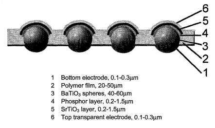
Figure 5 shows the schematic diagram of the proposed structure of
the Sphere-Supported Thin Film Electroluminescent (SSTFEL) device. A
phosphor layer 4 is deposited onto the top surface of BaTi03 spheres 3.
In a preferred embodiment a thin SrTi03 layer 5 is deposited onto the
phosphor layer for effective charge injection into the phosphor layer. The
BaTi03 spheres are embedded within a polymer layer 2 with the top and
bottom areas of the BaTi03 spheres exposed. The top area of the BaTi03
spheres and the surrounding polymer is coated with transparent
electrically conducting electrode 6; the bottom area of the BaTi03 spheres
and surrounding polymer is coated with another electrically conducting
electrode 1, which may be opaque. The preferred thickness ranges for
each of the components comprising the SSTFEL structure are shown to
the right of the corresponding components in Figure 5.
14
CA 02537476 2006-03-O1
WO 2005/024951 PCT/CA2004/001592
Any EL phosphor material may be used including but not limited to
metal oxide or sulphide based EL materials. For example, the sulphide
phosphor may be any one of ZnS:Mn or BaA12S4:Eu, or BaA14S7:Eu. The
oxide phosphors may preferably be any one of Zn2Sio.5Geo,504:Mn,
Zn~Si04:Mn, or Ga~03:Eu and CaA1204:Eu.
A specific embodiment of the SSTFEL structure that has been
fabricated and tested is shown in Figure 6. Isolated BaTi03 spheres 33 are
embedded in the polypropylene film 22, which does not cover the top and
bottom areas of BaTi03 spheres. The top surface area of the spheres is
coated with green oxide phosphor layer 44 which is Zn2Sio.5Geo.504:Mn.
SrTi03 was not deposited on the oxide phosphor layer. The whole bottom
surface area of the BaTi03 spheres and polypropylene film are coated with
a gold layer 11. The top transparent electronically conducting electrode is
deposited ITO layer 55. The thickness ranges for each of the components
are shown in Figure 6.
Details of a non-limiting, exemplary fabrication process will now be
provided.
Spray-dried BaTi03 particles used comprise NanOxideTM HPB-1000
Barium Titanate Powder (Lot# BTA020516AC), which is produced by TPL,
Inc. The particles had almost spherical shape, very smooth surface, and a
large size distribution range of approximately 1 ~120p,m. While spherical
particles are preferred, it will be understood that the particles do not need
CA 02537476 2006-03-O1
WO 2005/024951 PCT/CA2004/001592
to be perfectly spherical and for example may be slightly ellipsoidal or
flattened in shape.
Sintering of the as-received spheres was perFormed at 1120°C for 2
hours in air within an open-end furnace. The shrinkage due to sintering is
approximately 20%, grain size after sintering is 0.40.8 p,m and surface
roughness is less than 0.5p,m. Sintered BaTi03 spheres with size range of
53~63p,m were selected by U.S.A standard test sieves (Laval Lab Inc).
In order to make a specific positional arrangement of BaTi03
spheres embedded in the polypropylene film, a pattern of circular
depressions is used to hold BaTi03 spheres on an alumina substrate
during the sputtering, annealing and embedding processes. This pattern of
circular depressions on a high purity AI203 plate is shown in Figure 7. The
54 ~.m diameter, and 18 p.m deep pits are arranged to form an array of
closely-spaced 5 x 5 units. The horizontal and vertical distances between
each unit are 284 p,m and 246 p,m respectively. Each pit is 71 ~,m away
from another pit within one unit based on a Genre-to-centre distance. A
few BT spheres are intentionally arranged among units in order to facilitate
the subsequent embedding process.
To provide a sufficient bond for each BaTi03 sphere to stay in each
pit, a polymer is melted into each pit first. In order to keep the alumina
surface between pits from being covered by polymer, solid poly (a-
methylstyrene) [PAMS, Mw=80, 800, d=1.075] powder is used to
16
CA 02537476 2006-03-O1
WO 2005/024951 PCT/CA2004/001592
accomplish the patterning process, and is introduced into the pits and then
melted. The PAMS powder is prepared by mechanical pulverization of
PAMS pellets. Particle size is approximately in the range of 1 ~1 Op.m. It
has no specific melting point. There is a temperature range (~ 50°C)
between softening point and fully melted state.
At room temperature, solid PAMS powder is put into each pit and
there is little PAMS powder on the surface area among pits. Then, still at
room temperature, BaTi03 spheres are spread onto the AI203 plate to
form one layer of a closed packed pattern. After increasing the
temperature to 115°C, PAMS powder in each pit forms an adhesive gel.
When BaTi03 spheres are pressed gently, one sphere adheres to each
pit. After cooling to room temperature, excess BaTi03 spheres is brushed
away, leaving the same pattern of spheres as that of pits indicated in
Figure 7.
After patterning, the AI203 plate loaded with BaTi03 spheres and is
baked at 1000°C for 10 minutes in air to burn off the PAMS completely.
After baking, the spheres are still weakly adhered to the AI203 plate due to
weak bonding forces that result from the burn-ofF of PAMS. The sticky
force is large enough to keep the spheres stationary during the following
sputtering, annealing and embedding processes.
A 50 nm thick AI203 barrier layer was first deposited on the top area
of BT spheres by RF sputtering, followed by a green emitting
17
CA 02537476 2006-03-O1
WO 2005/024951 PCT/CA2004/001592
Zn2Sio.5Geo,5O4:Mn phosphor layer sputtered in the same chamber. The
spheres were kept at 250°C and the EL film thickness was about 800nm.
After sputtering, the spheres, still sitting on the AI203 plate, were annealed
at 800°C for 12 hours in vacuum with an oxygen pressure of 2.0x10⁻⁴
Torr.
This annealing procedure is to activate and crystallize the phosphor layer.
The AI203 barrier layer improves the phosphor performance since it acts
as a diffusion barrier between the BT and the phosphor.
After annealing, the procedure to embed phosphor-coated BaTi03
spheres into a polypropylene film is shown in Figure 8. A 25.4 p.m-thick
biaxially oriented polypropylene film (TRANSPROP TM OL polypropylene
from Transilwrap Company, Inc.) was placed over the phosphor-coated
BT spheres. Then a Gel-Pak sheet which comprises an elastic, gel-like,
adhesive polymer layer 1 supported by a polyester sheet 2 (GEL-FILM TM
WF-40/1.5-X4 from Gel-Pak Inc.) was placed on the top of the
polypropylene film. A pressure of 180g/cm2 was applied on the back of
polyester sheet to hold this structure together. After heating the whole
structure at 200°C for 5 minutes, the polypropylene film melted and
filled
in between the spheres under the pressure. After cooling, a pp-BT
composite sheet was peeled ofF. Next, this composite sheet was
sandwiched between two Gel-Pak sheets. Pressing the sandwich
structure under 180g/cm2, this composite sheet was heated and melted
again so that the pp moves to the centre of the composite sheet. Note
18
CA 02537476 2006-03-O1
WO 2005/024951 PCT/CA2004/001592
that the top and bottom areas of the spheres are not covered by
polypropylene film. The adhesive layer of the Gel-Pak film is elastic and
deforms under pressure. It can effectively protect the top and bottom area
of the spheres from being covered with polymer. Moreover, the resultant
polypropylene film could be easily peeled off from this Gel-Pak adhesive
layer without any damage.
After the resultant film of Figure 8c was obtained, a thin layer of
gold (100nm) was sputtered onto the bottom area of the film. A
transparent ITO electrode (100nm) was sputtered onto the top area of the
film. When an AC voltage of between 150 and 300 volts peak was applied
across the ITO and gold electrodes, bright green light was emitted from
the top area of the spheres:
It can be seen that the exposed top and bottom areas of the BT
spheres are symmetric with the pp film. The thickness of the composite
film is dependent on the original pp film thickness, BT sphere density,
applied pressure and other processing parameters during the embedding
process.
When an AC applied voltage is above the threshold value across
the ITO and gold electrodes, the phosphor-coated top area of each
individual BT sphere emits green EL. It is observed in prototype devices
that the light-emitting area varies in each BT sphere due to variations of
19
CA 02537476 2006-03-O1
WO 2005/024951 PCT/CA2004/001592
the size of BT spheres and the uniformity of the pp-BT composite film
which also affects the size of the light-emitting area.
Figure 9 shows the average luminance and luminous efficiency as
a function of peak applied voltage. The frequency of the driving voltage is
60Hz. Average luminance of the SSTFEL device could reach 35 cd/m2
driven at 250 volts. The highest luminous efficiency is about 0.18 Im/W.
When driven at 600Hz, luminance reaches over 150 cd/m2 as shown in
Figure 10.
It should be noted that a transparent, thin film dielectric layer
deposited on top of the phosphor layer is generally understood to improve
the EL characteristics, and should be considered as within the scope of
this invention. As mentioned above, although an oxide EL phosphor was
used in some of the examples disclosed herein, other EL materials may
be used such as sulphide phosphors.
The spheres may also be coated by thin film phosphor and
dielectric layers using other methods. For example, instead of sputtering,
films may be grown by evaporation or chemical vapour deposition
techniques.
Rather than only coating the top portion of the spheres, the thin film
EL phosphor and thin film dielectric layers may be coated uniformly on the
entire surface of the spheres. This may be achieved by rolling the
spheres during deposition, or by using a chemical vapour deposition
CA 02537476 2006-03-O1
WO 2005/024951 PCT/CA2004/001592
process with the spheres in a fluid bed allowing the vapour stream to pass
through the bed. After embedding the spheres into the polymer substrate
the portion of the spheres protruding from the back of the polymer film
may be etched in a weak acid, for example, to remove the thin films in this
region, resulting in a structure very similar to that shown in Figure 7. The
advantage of this approach would be that the coated spheres would not
require any orientation prior to being embedded into the polymer; and
could therefore be prepared as a loose powder. If the etching step is
omitted, light will be generated at both the upper and lower phosphor
areas of each spheres.
Dielectric materials other than barium titanate could be employed to
make spheres such as strontium titanate (SrTi03) and lead zirconium-
titanates (Pb(Zr,Ti)03), for example. Th'e diameter of the spheres could be
as small as about 5 microns or as large as about 500 microns.
Polymers other than polypropylene could be employed. Possible
materials include polyethylene, polystyrene or polyester. In general,
electrically insulating polymers capable of bonding to the spheres and
being coated with electrode layers could be employed. For maximum
contrast, or for specific applications black or coloured polymers could be
considered, to give the resulting EL device a specific black or coloured
appearance.
21
CA 02537476 2006-03-O1
WO 2005/024951 PCT/CA2004/001592
Spheres emitting several different colours could be deposited into
the polymer in a spatially patterned manner. For example, red, green and
blue emitting EL phosphors are known, and could be arranged in pixels to
form an array of picture elements capable of representing colour images.
Each pixel could consist of one sphere emitting each colour, or of many
spheres emitting each colour. By depositing row and column electrodes
appropriately placed relative to the various colour-emitting regions of the
EL device, a colour EL display that can be addressed electronically may
be realized, see Figures 12 to 14 showing details of fabricating such EL
display arrays.
Patterning of the spheres of various colours could be achieved
using well known printing methods for inks and toners. These include silk-
screening and printing from metal plates, as well as the photocopying
processes in which electrically charged toners are electrostatically
patterned by means of a photosensitive plate or drum.
Spheres emitting various colours could be blended to achieve a
desired pre-selected colour due to the combination of two or more colours.
Additional protective layers of suitable materials such as polymer or
glass sheets could be added above and below the EL device to provide
electrical protection or to provide for a sealed device.
An improvement to the device of Figure 5 may be made as shown
in Figure 11. In this embodiment, a more complex ITO electrode is used
22
CA 02537476 2006-03-O1
WO 2005/024951 PCT/CA2004/001592
which prevents undesirable high electric fields that may develop across
the polymer in the regions near the phosphor coated surface of the BT
spheres. This ITO coating could be deposited using, by way of example,
the following process: Firstly, the phosphor 4 coated spheres 2 could be
embedded into the polymer sheet 3 such that almost half the spheres
protruded on the front side of the polymer sheet. A first transparent ITO
top electrode 6 is then be sputtered onto one side of the spheres, and
subsequently the spheres are embedded symmetrically such that the front
and back of each sphere were equally protruding. Then a second
transparent ITO top electrode 7 in electrical contact with the first
transparent ITO top electrode would be sputtered. Finally, a bottom
electrode 1 would be sputtered to form the structure of Figure 11. The use
of both front electrodes at 6 and 7 prevents high electric fields from being
present in the polymer during electrical operation of the device.
It is also anticipated by the inventors that alternative uses of the
spherical structures provided herein exist. For example, referring to
Figure 7b, if the BaTi03 .is replaced with an n-type semiconductor, and the
phosphor layer were replaced with a p-type semiconductor, then a p-n
junction diode device could be formed in each sphere. A semiconductor
of interest could be GaXln~~_X~N which is known to provide for efficient light
emission in diode devices.
23
CA 02537476 2006-03-O1
WO 2005/024951 PCT/CA2004/001592
The portion of the spheres protruding from the back of the polymer
film could also be used to advantage. For example, a thin film of a
suitable semiconducting material could be grown such that it provided
switching characteristics to improve the matrix addressing properties of a
display device which had many row and column electrodes. Other
switching devices could also be formed by a patterning process on the
said portion of the spheres to create circuitry capable of controlling the
electric current flowing through each sphere, or allowing each sphere to
become a device that could store information relevant to its brightness
level.
In the examples presented above, the portions of the spheres
protruding from the front and back of the polymer film were about equal in
area. However if in FIG 8b) the elastomer layers of two Gel-Pak sheets
had different elastomeric characteristics, it would be possible to provide
for different areas of the portions of the spheres protruding from the front
and back of the polymer film. This could be used to optimize display
performance or properties.
All the above description relates to visual display applications of
this technology. With appropriate modifications, other applications could
include flexible capacitors. The capacitor would be formed as shown at 50
in Fig. 11, but would differ from the EL device in that the transparent
electrode 6 on the top of the spheres/polymer film (Figure 5) would be
24
CA 02537476 2006-03-O1
WO 2005/024951 PCT/CA2004/001592
replaced by a metal electrode and there would be no phosphor layer. The
completed capacitor can now be laminated onto a printed circuit board, or
,even within the layers of a printed circuit board to realize an integrated
capacitor. A review of other approaches to the integrated capacitor (R.
IEEE Spectrum Magazine, July, 2003, pp26-30) generally involve the use
of a glass or ceramic layer deposited on a metal foil which can crack and
therefore fail, whereas this invention avoids this problem by the natural
flexibility of the polymer film between the ceramic spheres. Generally high
values of capacitance may be achieved using high dielectric constant
ceramics such as BaTi03 for the spheres. The diameter of the spheres
may also be small, such as 10 p,m, to further increase capacitance. In
many cases only low voltages of 1-5 volt need to be applied to these
capacitors, permitting the use of smaller spheres and a correspondingly
thinner polymer film. These capacitors could be used in printed circuit
boards (i.e. incorporated as a dielectric layer within the circuit board
laminate) for circuit applications requiring a high performance capacitor
that doesn't occupy circuit board space like a regular capacitor mounted
on the board. In addition, since leads between the capacitor and the
circuit board are eliminated, the usual parasitic inductance associated with
the capacitor is minimized.
As used herein, the terms "comprises" and "comprising" are to be
construed as being inclusive and open ended, and not exclusive.
CA 02537476 2006-03-O1
WO 2005/024951 PCT/CA2004/001592
Specifically, when used in this specification including claims, the terms
"comprises" and "comprising" and variations thereof mean the specified
features, steps or components are included. These terms are not to be
interpreted to exclude the presence of other features, steps or
components.
The foregoing description of the preferred embodiments of the
invention has been presented to illustrate the principles of the invention
and not to limit the invention to the particular embodiment illustrated. It is
intended that the scope of the invention be defined by all of the
embodiments encompassed within the following claims.
26