Note: Descriptions are shown in the official language in which they were submitted.
CA 02537549 2006-03-02
Digital Signal Processing Device
The invention relates to a digital signal process-
ing device, in particular a digital computing device,
according to the preamble of claim 1.
In digital signal processing, digital signals are
digitally processed by applying various algorithms, the
digital signals being derived e.g. from originally ana-
logue signals by scanning. Signal processing may, e.g.,
be in form of computations corresponding to algorithms
used in communications engineering, e.g. in order to
realize a band pass filter or the like. For such digi-
tal signal processing, the digital signal values are
stored in binary form in memory means, the values
mostly being stored as an integer in 2-complement rep-
resentation or as fixed point format. With certain ap-
plications, also the more complex floating point format
can be resorted to.
For carrying out the digital signal processing,
mostly digital signal processors (DSP) are used, in ap-
plications with very high throughput rates, such as,
e.g. in the course of an image compression or in the
DSL (digital subscriber line) technique, also specially
tailored arithmetic-logic units are used which allow
- 1 -
CA 02537549 2006-03-02
for substantially higher computing speeds.
In the course of signal processing, often a format
conversion is necessary, i.e. the number representation
must be changed with a view to the precision desired.
What is typical in this instance is that for a higher
precision, the number of the bits used, i.e. the bit
width of the data words, must be extended, with a re-
duction being required again thereafter, and moreover,
during these format changes also the position of the
decimal point must be adapted. With these format align-
ments and decimal point adaptations, naturally numeri-
cal errors will result which, subsequently, will also
affect the precision of the result and, thus, the qual-
ity of the output signal; in applications in the field
of communication technology, the reduced quality of the
output signal may, e.g. show itself as signal noise,
and, e.g. when realizing (designing) integrating fil-
ters, a total failure of these filters can be caused.
Accordingly, the exact format alignment as well as
optionally also a rounding which is correct with regard
to such a digital signal technology are highly critical
aspects in the course of such a digital signal process-
ing, such manipulations, moreover, occurring frequently
in the common practical applications as an addition to
- 2 -
CA 02537549 2006-03-02
the mathematical computations proper, such as multiply-
ing or adding. Therefore, such a format alignment also
has substantial effects on the processing speeds ob-
tamable, i.e. the clock frequency which can be
achieved in each case, whereby consequently also the
technical and economical chance of implementation will
be determined.
In the signal processors currently used, or known,
respectively, format adaptations and roundings are ef-
fected in terms of program technology by means of a se-
ries of individual commands, wherein several clock cy-
cles are required for carrying out these commands; in
some cases, the number of clock cycles required there-
for may be larger than the number of clock cycles for
the algorithmic signal processing or computation
proper, which, of course, is particularly disadvanta-
genus.
From US 4,041,461 A, US 4,876,660 A and
US 5,844,827 A, processor devices are known in which
also re-formatting is carried out in the course of sig-
nal processing procedures. In the known techniques,
however, the information for a re-formatting is pro-
vided in concrete manner a priori due to an appropriate
programming via a control processor, and deposited in a
- 3 -
CA 02537549 2006-03-02
register, i.e. here, the respective shifting operations
must be provided in detail by programming, transition
to other number formats requiring corresponding new
programming inputs. These known techniques thus are in-
flexible and unhandy with regard to format changes.
Accordingly, it is an object of the invention to
provide a particularly efficient processing of digital
signals by employing flexible number format alignments
and, optionally, rounding operations, wherein in par-
ticular an arbitrarily presettable format alignment
shall be rendered possible within a single clock cycle,
and this even in the same step as the mathematical op-
erations proper.
To achieve this object, the invention provides for
a digital signal processing device comprising the fea-
tures of claim 1. Particularly advantageous embodiments
and further developments are defined in the dependent
claims.
Thus, in accordance with a particularly preferred
aspect of the invention, a specific format alignment
unit, preferably including a rounding unit, is directly
integrated in the data path of the arithmetic-logic
unit. The possible format alignments as well as, op-
tionally, rounding operations thus become a direct com-
- 4 -
CA 02537549 2006-03-02
ponent of each signal processing command so that, as a
rule, no separate clock cycle is necessary. A further
advantage consists in that program furnishing is sub-
stantially simplified since the programmer automati-
cally is no longer confronted with the problems arising
in connection with format alignment. The number format
alignment unit, optionally with the integrated rounding
unit, need not be designed for a previously determined
format, much rather it is possible with particular ad-
vantage to pre-set a format or adjust a format, for
which purpose preferably, a format-register is provided
as format-presetting unit. This format register is
charged once as required, and then, on account of its
contents, it will determine the format alignments and
roundings and, thus, the exact mode of functioning of
these units. In particular, the format register con-
tams arrays for determining the data format, such as
the number of digits as a whole and the number of the
digits following the decimal point, this being so both
for the source format and for the destination format.
Furthermore, also a saturation function (also
termed clipping function) can be integrated in the num-
ber format alignment unit so as to prevent an overflow
of a signal value when exceeding the maximum value into
_ 5 _
CA 02537549 2006-03-02
the reverse algebraic sign. By integrating such a satu-
ration function, i.e. incorporating a saturation unit
in the format alignment unit, it is also achieved that
no additional clock cycle will be required, and, as has
been mentioned, errors which could possibly arise in
connection with the format alignment and the rounding
function, are prevented by this saturation function. A
comparable saturation function preferably is also asso-
ciated with the rounding unit to thus recognize a pos-
Bible overflow when rounding up, and to output the cor-
rect result.
In the following, the invention will be explained
in more detail by way of preferred exemplary embodi-
ments to which, however, it shall not be restricted. In
detail, in the drawings:
Fig. 1 shows a block diagram of a signal processor
known per se;
Fig. 2 shows a schematic block diagram of an
arithmetic-logic unit of such a processor, i.e. with a
number format alignment unit according to the inven-
tion, which has an associated format presetting unit;
Fig. 3 shows such an algebraic-logic unit with
number format alignment unit in more detail;
Fig. 4 schematically shows a format of a format
- 6 -
CA 02537549 2006-03-02
register as a format-presetting unit;
Fig. 5 shows a detailed set-up of the number for-
mat alignment unit including rounding unit and satura-
tion unit, in two partial figures 5A and 5B which be-
long together;
Fig. 6 shows a table with positive and negative 4-
bit binary numbers having algebraic signs associated to
them, with a value range of from -8 to +7;
Fig. 7 shows a comparable table with 4-bit binary
numbers, each having two digits in front of the decimal
point and two digits thereafter, the values ranging
from -2 to +1.75;
Fig. 8, in association with the arrangement of
Fig. 5, schematically shows an example of a number for-
mat alignment with rounding and saturation, having an
overflow; and
Fig. 9 shows a comparable example of a number for-
mat alignment with rounding and saturation, but now
with an underflow.
In Fig. 1, the construction of a processor known
per se is schematically illustrated in a block diagram,
wherein a program memory 1 is provided, to which a pro-
gram controller 2 is connected so as to appropriately
control an arithmetic-logic unit 4 that receives the
7 -
CA 02537549 2006-03-02
data to be processed from a data memory 3. What is
known for the design of such arithmetic-logic units 4
are the Harvard-architecture, as illustrated, or also
the Von Neumann-architecture; here it is proceeded from
an arithmetic-logic unit 4 of Harvard architecture,
even if this, of course, is not to be seen as restric-
tive. The arithmetic-logic unit 4 quite generally con-
tams an arithmetic unit (ARU) as will be explained in
more detail hereinafter by way of Fig. 3, and it de-
fines a data path.
In such a digital signal processor, each program
instruction is carried out in three phases, the control
of the sequence being effected by means of the program
control 2. In the first phase, the so-called fetch
phase, a command word is read out of the program memory
and supplied to the program control 2, as illustrated
in Fig. 1 by reference 1a. In the subsequent decode
phase, this command word is decoded and split up into
individual micro-operations, by which the arithmetic-
logic unit 4 is activated. This is indicated by connec-
tion 2a between the program control 2 and the arithme-
tic-logic unit 4 in Fig. 1. In the third phase, the
execute phase, the instruction is operated, and accord-
ingly, in this phase the micro-operations are transmit-
- g -
CA 02537549 2006-03-02
ted in the form of control signals via the connection
2a to the arithmetic-logic unit 4 to be actually car-
ried out, data from the data memory 3 being addition-
ally loaded into the arithmetic-logic unit 4 via the
data connection 3a; in the arithmetic-logic unit 4,
these data are arithmetically processed and temporarily
stored in registers. After this processing, the data
obtained are, e.g., stored again in data memory 3, e.g.
via a connection 4a. In this respect, the data memory 3
constitutes, e.g., an input storage means and, at the
same time, an output storage means for the arithmetic-
logic unit 4.
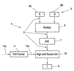
In Fig. 2, the construction of an arithmetic-logic
unit 4 is shown in somewhat more detail in a block dia-
gram, wherein data A, B to be interlinked are supplied
to input registers 5A, 5B, e.g. (for instance from the
data memory 3 according to Fig. 1), which can be con-
sidered as an input memory means 5, whereupon the data,
when running the said micro-operations, get into the
arithmetic unit, and here, e.g., a multiplier unit 6 is
provided in series with an adding unit 7. The result of
these calculation operations will normally be supplied
to output memory means, here schematically illustrated
by a result register 8, the result being indicated by
g
CA 02537549 2006-03-02
"Y". The individual components 5A, 5B to 8 define a
data path 9, and in this data path 9, a number format
alignment unit 10 is directly arranged which simultane-
ously contains a rounding unit, as will be explained in
more detail hereinafter. This data format alignment
unit 10, alignment unit or also adapting unit termed in
short hereinafter, is capable of converting the data
supplied into a pre-determined number format, wherein,
as shown in Fig. 2, a format presetting unit 11 is pro-
vided which, in particular, has the form of a format
register, and whose output is connected to the align-
ment unit 10, as indicated in Fig. 2 by connection 11a.
This format presetting unit 11 can be loaded with ap-
propriate format information for the respective calcu-
lating procedure or data processing procedure, as sche-
matically indicated at input 11b in Fig. 2.
Arranging the alignment unit 10 directly in the
data path 9 leading from the input registers 5A, 5B to
the result register 8 in the manner illustrated means
that the desired format alignments and, optionally,
rounding operations can occur in the same clock cycle
in which the calculating operations are carried out,
with only a short delaying time having to be put up
with until the data will appear at the output of the
- 10 -
CA 02537549 2006-03-02
alignment unit 10. This means a temporal acceleration
in comparison with a technique in which the format
alignments and rounding operations are carried out via
the program such that they will only occur in subse-
quent clock Cycles, after the calculating procedures
proper, in separate alignment and rounding steps of the
program. The present hardware-type realization of these
alignment and rounding tasks directly in the data path
9 also allows for a simplification of programming,
since in the respective program to be stored in program
memory 1 in Fig. 1, simply the desired formats must be
provided for storage in the format presetting unit 11
(as far as these formats do not result by themselves a
priori from the memory format of the data memory 3),
yet no alignment and rounding operations whatsoever
need to be programmed. In case the previously referred
to delaying time that must be taken into consideration
in the present technology were rather long in compari-
son with the clock time, e.g. in case it should take a
half clock cycle, which might possibly happen in par-
ticularly fast arithmetic-logic units 4 with particu-
larly short clock cycles, it may very well be provided
for a memory element (register) for buffer purposes to
be incorporated in the alignment unit 10, so that then
- 11 -
CA 02537549 2006-03-02
the format alignment and rounding activities started in
the given clock cycle can be finished in a second clock
cycle, without the given delaying times possibly nega-
tively affecting the result of the operations in the
arithmetic-logic unit, as is deposited as result Y in
register 8.
From Fig. 3, further details for the construction
of such a typical arithmetic-logic unit 4 for DSP
(digital signal processor) applications are apparent.
In digital signal processing, an important task is, for
instance, the so-called multiply-accumulate function
(MAC function). In this function, two input numbers
(operands) are multiplied, and the result of the multi-
placation then is added to the content of an accumula-
tor. Such a MAC function is realized by the arithmetic-
logic unit 4 according to Fig. 3, e.g., wherein, more-
over, the result obtained is subjected to number range
adaptation (number format alignment and rounding). For
such functions, often the 2-complement representation
with algebraic signs is used for the numbers, as will
be explained in more detail hereinafter by way of Figs.
6 and 7, with the invention, however, naturally not be-
ing restricted to such a representation. To simplify
matters, however, the entire following description has
- 12 -
CA 02537549 2006-03-02
been based on such a 2-complement representation with
algebraic signs.
According to Fig. 3, in the beginning the desired
numbers A, B for the multiplication to be carried out
are read out of data memory 2 and loaded into registers
5A, 5B, which is effected by the program control (pro-
gram control 2 in Fig. 1) by means of the respective
loading commands "LOAD". In comparable manner, the data
memory 3 moreover is supplied with "CONTROL" control
commands from the program memory 2 via a control line
3b. In the next step, the data, or operands, respec-
Lively, A, B are then supplied to the arithmetic unit
6, a corresponding control signal (MUL/DIV - multi-
ply/divide) being applied to the former by the program
control 2 at 6b. The result of the multiplication is
supplied to the adder/subtracter 7 via connection 6a,
to which an adding command (or subtracting command, re-
spectively; ADD/SUB) is supplied accordingly by the
program control 2 via a control connection 7b. From the
output of an accumulator 12, the current content of
this accumulator 12 is supplied to a second input of
this adder/subtracter 7, as indicated at 12a in Fig. 3.
The result of this addition is again stored in accumu-
lator 12, compare the output 7a of the adder 7, with a
- 13 -
CA 02537549 2006-03-02
multiplexes 13 being interposed which, via a control
input 13b ("SELECT"), is adjusted such by the program
control 2 that the multiplexes 13 will bring the adder
output 7a to the respective input of the accumulator 12
(cf. link 13a between multiplexes 13 and accumulator
12). Operation of the accumulator 12 is initiated by a
control input 12b ("OPERATION") coming from the program
control 2.
The multiply/accumulate command usually is re-
peated several times in a loop; as soon as the final
result is present in the accumulator 12, it is, in the
present example, stored again in data memory 3,
wherein, however, the number format is adapted before,
since the width of the accumulator 12 as a rule is lar-
ger than the width of the data values A, B read out of
data memory 3. In the present example, the multiplexes
13 serves to load the accumulator 12 with an initial
value from the data memory 3 by means of a separate in-
struction at the beginning of a loop. Usually, the
value "00" is used as this initial value.
As has been mentioned, the contents of accumulator
12 (output 12a) thus is transferred to the alignment
unit 10 for number format alignment and, preferably,
also for a possible rounding, before it is re-stored in
- 14 -
CA 02537549 2006-03-02
data memory 3, and in this alignment unit 10 the adap-
tation of the number format and the rounding are car-
ried out, as is to be described in more detail by way
of Fig. 5. By this, it is achieved that the calculation
result will correspond to the pre-determined memory
format, wherein, nevertheless, a greater word width
(number width, i.e. a larger amount of bits per number)
can be used for the calculation processes carried out
in the arithmetic-logic unit 4, for a higher precision
of computation. The respective control information is
received by the alignment unit 10 from the format pre-
setting unit 11, preferably a register which contains
control data regarding the respective fixed format
(FXD FORMAT); this control information is loaded be-
forehand, at the start of the program, during an ini-
tializing phase, in accordance with the memory format
presetting of the data memory 3, e.g.. To this end, for
instance at the start of the program, a value is di-
rectly read out of the data memory 3, cf. output 3a in
Fig. 3, and loaded into the presetting unit 11 with the
help of a control signal 11b (~~LOAD"). This word, thus,
indicates the destination format (DST - destination)
which the obtained result Y (cf. Fig. 2) shall have,
wherein the format pre-setting unit, or register 11,
- 15 -
CA 02537549 2006-03-02
respectively, contains an appropriate region DST, apart
from a memory region SRC (SRC - source) for respective
format data regarding the format used during the calcu-
lation operation in the arithmetic-logic unit 4. The
appropriate format data can have a length of 8 bit each
in the register 11 (cf. the bit digits 0-7, a total of
0-15, in the presetting unit 11 according to Fig. 4).
The format SRC in presetting unit 11 thus relates
to the format of the number given at the output of ac-
cumulator 12, the "source number", whereas the format
DST indicates the destination format of the data word
for storing in data memory 3. Each field DST, SRC, re-
spectively, in register 11 contains the position of the
decimal point in the form of a binary number without
algebraic sign, a value of "2", e.g., indicating that
the number to be regarded shall have two decimal
places, i.e. two digits to the right from the decimal
point, so that the decimal point will be shifted from
the outermost right position by two digits to the left.
According to Fig. 3, the alignment unit 10 deliv-
ers the result (Y; cf. also Fig. 2) at its output 10a
proper, which result will be deposited in the output
memory means, according to Fig. 3 directly in data mem-
ory 3; in addition, during the format alignment and
- 16 -
CA 02537549 2006-03-02
rounding, also an overflow or an underflow may result
during the adaptation of numbers (underflow - UFL;
overflow - OFL), and respective status signals UFL and
OFL are provided at outputs 10b and 10c of the align-
ment unit 10; these two status signals UFL, OFL can
preferably be supplied to a status register 14 so as to
be available for a treatment of exceptions.
With reference to Fig. 5, the mode of operation of
the alignment unit 10 (format alignment, rounding)
shall be explained now in more detail, wherein in the
following, it will be referred to Figs. 6-9, too. Fig.
5 is composed of Figs. 5A and 5B, which are to be imag-
fined to be laid at each other along the broken separat-
ing lines in Figs. 5A and 5B. Fig. 5, moreover, also
contains exemplary dimensional data regarding the num-
ber of bits and width of bits of the individual data
values incurred in the course of processing, these di-
mensional data being very much in line with common
practical examples. Subsequently, to provide for a bet-
ter understanding, further explanations shall be given
by way of concrete, yet simplified numerical examples
with low bit numbers, making particular reference to
Figs. 8 and 9, wherein also previously 2-complement
number representations shall be explained by way of
- 17 -
CA 02537549 2006-03-02
Figs. 6 and 7, with regards to overflow and underflow.
The alignment unit 10, also termed ALIGN and ROUND
unit (with a view to the format adaptation and round-
ing), is provided with the output value 12a of accumu-
lator 12, as already mentioned, and as is also visible
in Fig. 5 in addition to Fig. 3. The format of this
output value at output 12a of the accumulator 12 subse-
quently is to be adapted by the alignment unit 10 ac-
cording to the specification by register 11 (termed
general format presetting unit 11) such that the data
word finally obtained (output 10a) is suitable for
storage in data memory 3 (or in any other data memory,
optionally with a different number format). The align-
ment unit 10 is arranged directly in the data path (cf.
data path 9 in Fig. 2) of the arithmetic-logic unit 4,
i.e. normally the operations carried out by the align-
ment unit 10 are preferably carried out in the same
clock cycle as the calculating operations in the pre-
ceding arithmetic units 6, 7, wherein only a slight de-
laying time occurs from step to step. However, in case
extremely short clock cycles were given, and the
switching modules by which the individual components,
in particular the alignment unit 10, are realized,
should cause a comparatively somewhat too large delay,
- 18 -
CA 02537549 2006-03-02
a buffer storage, as has already been mentioned, can be
provided within the alignment unit 10, optionally also
upstream and/or downstream of the alignment unit 10, to
thereby carry out a first part of the operations in a
first clock cycle, and a second part in a second clock
cycle. In Fig. 5, however, such a buffer memory unit
(in particular, a register) to be interposed has not
been drawn, since normally, such buffering is not re-
quired, but much rather the calculation operations as
well as the format alignments can be effected in one
and the same clock cycle.
As an integral hardware-type component, the pre-
sent alignment unit 10 contains also a rounding unit 15
which consists of individual logic modules and an ad-
der, as will be explained in more detail hereinafter;
furthermore, a so-called saturating function is inte-
grated to prevent a change of the algebraic sign in
case of a number overflow, or underflow, respectively,
see also the following explanations in connection with
Figs. 6 and 7.
In the Example according to Fig. 5, the accumula-
for 12 has a width of 80 bits (cf. the bit locations
No. 0-79 in Fig. 5A), and in the alignment unit 10, an
alignment into a number having a width of 32 bits shall
- 19 -
CA 02537549 2006-03-02
be effected which corresponds to the width of a data
word in data memory 3. For this purpose, the format
register 11 in addition contains a value of 40 in the
SRC array (cf. Fig. 4), and a value of 16 in the DST
array, which means that the 80 bit number from accumu-
lator 12 (the SRC number, i.e. the source number) has
its decimal point to the right of bit No. 40, whereas
the 32 bit destination number (DST number) after the
adaptation, or alignment process, respectively, shall
have its decimal point to the right of bit No. 16.
At the start of data format adaptation, or align-
ment, respectively, the 80 bit number is extended on
both sides by means of an extension unit 16, i.e. by 32
bits on the right-hand side, the LSB (LSB - least sig-
nificant bit) side, i.e. by as many bits as the desti-
nation word DST has, these newly added 32 bits all be
ing set to "0". On the other side, the left-hand side,
the MSB (MSB - most significant bit) side, also 32 bits
are added for an extension, corresponding to the bit
width of the destination word, the value of this bit
being chosen according to the value of the algebraic
sign bit which is taken over from the accumulator 12,
i.e. the bit at position "79". This procedure is also
termed "sign extend", cf. also the bit frame SIGN (SRC)
- 20 -
CA 02537549 2006-03-02
of the extension unit 16 in Fig. 5A. On the whole, thus
a width of 32 + 80 + 32 - 144 bits, from bit No. 0 to
bit No. 143, is obtained, the bits at positions 32-111
forming the original number at output 12a of the accu-
mulator 12.
Subsequently, the decimal point must be adapted to
this number which has been extended to a total of 144
bits, this being done such that the decimal point will
come to lie exactly at the required position with a
view to the destination number at output 10a of the
alignment unit 10. Be it assumed that bit No. 0 in the
source number, i.e. at the output 12a of accumulator
12, as bit having the valency 2° is always positioned
to the left of the decimal point, so that this bit in
the source number is present at position "40", and in
the destination number (output 10a of the align unit
10) it should be located at position "16". Thus, a
"shifting" by (40-16=) 24 bits towards the right (ac-
cording to the illustration of Fig. 5A) must be ef-
fected. This shifting is effected with the help of
shift unit 17 ("SHIFT"), this shifting procedure to-
wards the right (by 24 positions) being schematically
illustrated by means of the oblique illustration of its
output 17a. At its control input 17b, the shift unit 17
- 21 -
CA 02537549 2006-03-02
which may be formed by a multiplexer control block,
e.g., will get the appropriate control information for
this shifting from a control unit 17' calculating the
amount of shifting. This control unit 17' will calcu-
late the amount of shifting from the values of the for-
mat presetting register 11 which are present at the
output 11a thereof and which are supplied to the con-
trol unit 17'. The calculated amount of shift results
from the difference between the decimal point positions
of the source format (SRC array in register 11) and the
destination format (DST array in register 11; cf. Fig.
4). In fact, the control unit 17' thus can consist of a
subtractor which forms the difference between the two
contents of arrays SRC and DST of register 11, and it
may also be directly integrated as a control stage in
the shift unit 17.
In Fig. 5, i.e. in Fig. 5A, the thus obtained bit
chain is schematically illustrated by a block 18,
wherein it is illustrated by broken, oblique lines that
the number originally derived from accumulator 12 has
now been shifted by an appropriate amount (i.e. by 24
bits) towards the right. During this shifting, the bit
positions cleared at the left side due to this shifting
must be filled according to the correct algebraic sign,
- 22 -
CA 02537549 2006-03-02
i.e. bits with the value of the algebraic sign bit of
the source number (bit No. 79 in accumulator 12) are
used for filling.
If, other than illustrated in Fig. 5, a shift to-
wards the left were required (so as to provide a larger
number of places following the decimal point), the bit
positions becoming cleared on the right side are filled
by "0"-bits.
Following this shift, the decimal point is already
at the correct position, corresponding to that in the
destination number, and the destination number can be
taken as a partial array from the entire word - i.e.
from the bit chain 18 - with the desired precision. In
the present case, the precision for the destination
number results from its width of 32 bits. The arrays of
the entire word are not changed, but merely interpreted
within the format of the destination number. This can
also be termed "mask change", and in Fig. 5 this opera-
tion has been illustrated by arrow 18A. The result
thereof is illustrated in Fig. 5 (more precisely, in
Fig. 5B) by partial array unit 19, wherein it is visi-
ble that the number array 19 DST proper (DST - destina-
tion - destination number) now has a width of 32 bits,
wherein to the left, 80 bits are contained in an alge-
- 23 -
CA 02537549 2006-03-02
braic sign array 19SIGN. On the right, at bit positions
"0" to "31", the bits for the locations to be cut off
(places following the decimal point) are contained,
simple cutting off corresponding to a rounding down,
wherein, however, under certain conditions, as will be
explained in more detail hereinafter, a rounding-up
will occur by means of the rounding unit 15. When re-
moving the bits for the destination number (output
19a), the given number range can be exceeded or fallen
short of. Exceeding is only possible if the source num-
ber was positive, falling short of only if the source
number was negative.
For recognizing a possible exceeding or falling
short of (overflow or underflow) of the number range, a
logic unit 20 is provided to which all 80 algebraic
sign bits of the algebraic sign array 19SIGN as well as
the algebraic sign bit of the destination word in the
destination word array 19DST (bit at location "31", in-
dicated by DST (32) in the drawing) are supplied via
connection 19b from the output of partial array unit
19. In case of a valid number in partial array unit 19,
all the algebraic sign bits are equal, i.e. either they
are all equal to "0", or they are all equal to "1". By
means of an OR gate 21 it is now recognized whether all
- 24 -
CA 02537549 2006-03-02
the bit positions of the algebraic sign array have the
value "0", and by means of an AND gate 22 it is deter-
mined whether all the bit positions of the algebraic
sign array have the value "1". The outputs of these
gates 21, 22 are applied to inputs of a checking block
23 which determines an overflow or an underflow if the
output signal (output 21a) of the OR gate 21 is not
equal to "0", or the output signal 22a of the AND gate
22 is not equal to "1". If the output signal 21a is not
equal to "0", or if the output signal 22a is not equal
to "1", the checking block 23 merely has to determine
whether an overflow or an underflow is present, and
this determination is carried out with the assistance
of the algebraic sign bit of the source number, as it
is contained in accumulator 12, cf. also the connection
12s to the checking block 23 in Fig. 5. If this alge-
braic sign bit (bit No. "79") has the value "0", an
overflow or an excess is present, and at the output 230
of checking block 23, a - preliminary - overflow signal
OFL will be activated. However, if the algebraic sign
bit has the value "1", there exists an underflow, and
at output 23u of the checking block 23, an underflow
signal UFL will be activated. This then also consti-
tutes the status signal UFL at output 10b of the align
- 25 -
CA 02537549 2006-03-02
unit 10 which has already been mentioned in the de-
scription of Fig. 3.
Yet, via a connection 23a, the evaluation result
of the checking block 23 is also delivered to a satura-
tion unit 24 which has a width of 33 bits, i.e. one bit
more than the width of the destination number, so as to
be able to recognize again a possible overflow after a
rounding addition to be described yet.
In accordance with the checking evaluation by the
checking block 23 (output 23a regarding UFL/OFL state),
the saturation unit 24 sets the number supplied at 19a
at its output 24a to the respective maximum final
value. More in detail, in case of an overflow (OFL)
this is the greatest positive number, i.e. in this
case, all the bits, with the exception of the algebraic
sign bit (bit Nos. 31 and 32) are set to "1", whereas
the algebraic sign bits at positions 31 and 32 are set
to "0". In case of an underflow (UFL), the "largest"
negative number (i.e. the negative number with the
highest absolute value) is delivered at output 24a,
i.e. in this output number, all the bits are set to the
value "0", with the exception of the two algebraic sign
bits Nos. 31 and 32, which are set to the value "1". As
has already been mentioned, a respective underflow sig-
- 26 -
CA 02537549 2006-03-02
nal, UFL, or overflow signal, OFL, is additionally de-
livered at outputs 10b, or 10c, respectively.
When cutting off the low-value bits (in the par-
tial array unit 19, to the right of destination word
array 19DST, i.e. the bits at locations Nos. 0-31), a
systematic error will arise, and when carrying out the
operations described several times (such as when re-
suits are accumulated in the course of filter realiza-
tions), these errors may sum up unfavorably and, possi-
bly, may have a total malfunction of certain algorithms
as a consequence. To counteract this, the aforemen-
tinned rounding unit 15 is provided which is to reduce
to 0 the systematic errors in the average. In practice,
e.g., the so-called IEEE rounding may be used (cf. eg.
IEEE Standard for Binary Floating Point-Arithmetic IEEE
754-1985). With this rounding, rounding ups are ef-
fected, and effected only, if at the positions follow-
ing the decimal point (the bit positions 0-31 here), at
least one "1" bit occurs somewhere in addition to a "1"
bit at position No. 31 (a single such additional "1"-
bit is sufficient), or if only bit No. 31 has the value
"1", and if also the LSB bit in the destination array
19DST has the value "1". Such rounding up means that,
with the help of an adder 25, a "1" (generally: the
- 27 -
CA 02537549 2006-03-02
smallest positive value) is added to the number ob-
tamed on the output of the saturation unit 24. A logic
unit 26 with an OR gate 27 and an AND gate 28 will rec-
ognize whether or not such rounding (rounding up, to be
precise) in fact has to be carried out. For this pur-
pose, the least significant bit (LSB bit) from the des-
tination word array 19DST (cf. connection 19c) as well
as the cut-off bits (cf. also connection 19d) are ap-
plied to the OR gate 27 whose output 27a is applied to
the AND gate 28 just as is the bit No. 31 of the cut-
off less significant bits (cf. output 19e). The afore-
mentioned IEEE rounding will provide for a rounding-up,
i.e. the adding of a "1" in adder 25 (output "1" of the
AND gate 28, connection 28a), if any bit 19d or 19c is
set to "1" and, at the same time, the bit 19e (bit No.
31 of the partial array unit 19) also has the value
"1"_
Such a rounding-up will, however, occur only if no
underflow (signal UFL) has been found by the checking
block 23, i.e. the adder 25 with one input also is con-
nected to output 23u of the checking block 23. If such
an underflow has not been found and rounding-up has to
be carried out, the adder 25 will add the smallest pos-
Bible positive number to the result in the output 24a
- 28 -
CA 02537549 2006-03-02
of the saturation unit 24.
Since such a rounding-up may again give rise to a
number overflow (OFL), a further saturation unit 29 is
connected to the output 25a of the adder 25, and this
saturation unit 29 delimits the output result (the des-
tination word) to the highest possible number value, in
the same manner as has been described by way of the
saturation unit 24. This highest possible number value
is delivered at output 29a and stored in register 30.
If there was no overflow, the number obtained from the
adder 25 will be directly written into register 30. In
case of an overflow, a corresponding OFL signal will be
delivered at the output 29b of the saturation unit 29,
and this OFL signal will be combined with the OFL sig-
nal at the output 230 of checking block 23 according to
an OR function, cf. the OR gate 31 in Fig. 5B, so that
also in case of just one overflow, a corresponding OFL
signal will be obtained at the output 10c of the align
unit 10.
From what has been said it can be seen that if
there is no overflow and no underflow of the number
during the return to the partial array (cf. partial ar-
ray unit 19), the units 24, 25 and 29 will remain with-
out function, and the output number 19a of the partial
- 29 -
CA 02537549 2006-03-02
array unit 19 will get directly to the register 30 (as
output memory means) and be stored there.
With this, the number format alignment and the
possible rounding has been finished, and the final re-
suit, i.e. the destination number DST, with the desired
bit width (corresponding to the bit width of the desti-
nation number array 10DST of the partial array unit 19)
now can be written into the general data memory 2 as
the result Y, as previously explained particularly by
way of Figs. 1 and 3. On the other hand, the status
signals UFL and OFL are not loaded into the status reg-
ister 14 (cf. Fig. 3).
For supplementation purposes, the so-called 2-
complement illustration of the binary numbers shall
shortly be explained by way of Figs. 6 and 7 as an ex-
ample, since the operations according to Fig. 5 have
been based on this 2-complement illustration. In Fig.
6, 4-bit binary numbers having an algebraic sign S are
illustrated in a table, and in that example, the value
ranges from -8 to +7. The positive numbers are shown at
P, the negative ones at N. As may be seen, if the alge-
braic sign S has the value ~~0", the number is positive
(wherein also the number 0 shall be counted among the
positive numbers); if, however, the algebraic sign S is
- 30 -
CA 02537549 2006-03-02
"1", the number is a negative number N. When adding or
subtracting, it may now happen that the limits of the
range of numbers are exceeded or fallen short of, re-
spectively, cf. the arrows 40 and 41 in Fig. 6. For in-
stance, when adding a positive number to a positive
number (cf. arrow 40), the range P of the positive num-
bers may be exceeded (overflow) so that a negative num-
ber will "form", since the bit word "0111" (for the
number +7) in the binary number illustration shown, is
followed by the number "1000", which, however, already
is the greatest negative number (-8). Similarly, if a
negative number is added to a negative number (in terms
of its amount) (cf. arrow 41 in Fig. 6), a positive
number may be formed (i.e. with a "0" at the position
of the algebraic sign bit S), resulting in an underflow
or a falling short of the range of values.
Also in Fig. 7, 4-bit binary numbers with an alge-
braic sign (again in the 1St column of the bits) and
having integer portions I (I-integer) and two places F
following the decimal point (F-fraction) are illus-
trated, the range of values of these binary number be-
ing from -2 to +1.75. When the IEEE rounding as previ-
ously mentioned by way of Fig. 5 is used as a basis,
the numbers +0.75, + 1.5 and +1.75, e.g., would be
- 31 -
CA 02537549 2006-03-02
rounded up to +1, +2, or +2, respectively, the places
following the decimal point should be cut off; there
would be no rounding-up with the number +0.5. Namely,
with this IEEE rounding, the number 0.5 is rounded
down, whereas 0.51 is rounded up already, and likewise
the number 1.5 is rounded up, yet not the number 2.5,
but number 3.5 will be rounded up again, etc.
In Figs. 8 and 9, examples with format alignment
and rounding, once with an overflow (Fig. 8), and once
with an underflow (Fig. 9), are illustrated in the form
of simplified bit illustrations shown in lines (1) to
(8) (with substantially smaller bit widths as compared
to Fig. 5).
In detail, the 1St line in Fig. 8 shows an 8-bit
source number SRC which comprises an integer 4-bit por-
tion and 4-bit places following the decimal point. The
outermost left bit in the integer portions is the alge-
braic sign bit S. The destination number DST illus-
trated in the 8th line, on the other hand, consists of
6 bits, wherein the first three bits represent the in-
teger portions including the algebraic sign bit, and
the further three bits represent the places following
the decimal point. The value of the source number SRC
amounts to +7.9375, which here corresponds to the larg-
- 32 -
CA 02537549 2006-03-02
est value that can be represented.
According to line (2), an extension is effected to
the left of the algebraic sign bit S, wherein the same
number (i.e. six) of bits (here "0" bits) is put up in
front as the number of bits of the destination number
DST. At the same time, just as many "0" bits (i.e., six
"0" bits) are added at the right side of the source
number SRC.
For the shift now required, the difference between
the number of places following the decimal point of the
source number SRC and that of the destination number
DST must be calculated (which is effected by the con-
trol unit 17 according to Fig. 5), and this difference
is "1" in the example of Fig. 8, i.e. the bit-chain is
shifted by one digit towards the right, cf. line (3) in
Fig. 8; in doing so, at the left side it is filled up
with the value of the algebraic sign bit, i.e. specifi-
cally a "0" bit is added here. Subsequently, according
to line (4) in Fig. 8, a new mask, now having merely
six digits according to the number of bits of the des-
tination number DST, is placed over this chain. Here,
this mask can be seen in Fig. 8 by a shorter block (as
compared to lines (1) to (3)). As may be seen, by this,
the 6-bit number in the 4th line of Fig. 8 becomes
- 33 -
CA 02537549 2006-03-02
negative ("1"-bit at the outermost left position). The
nine bits to the left thereof (including the algebraic
sign bit of the destination number) are now checked for
their uniformity, and since they are not all equal, an
underflow/overflow condition is determined, cf. the
logic unit 20 in Fig. 5. To determine with exactness
whether an overflow or an underflow exists, the alge-
braic sign bit of the source number SRC is used; this
algebraic sign bit has the value "0" in the present
case, so that an overflow (OFL) is determined. If the
algebraic sign bit of the source number SRC had the
value "1", an underflow would be determined. With the
help of the saturation unit 24 (Fig. 5), the destina-
tion word DST now receives the highest positive value,
as is visible from the 5th line in Fig. 8, where this
value now is +3.875. At R in Fig. 8, the rounding unit
15 (cf. Fig. 5) recognizes the necessity of rounding
up, and for this the rounding unit 15 employs the seven
bits standing to the utmost right. Accordingly, the
destination number DST is incremented by the value
0.125 (the smallest value that can be represented with
three bits), and this addition value is illustrated in
the 6th line of Fig. 8, whereas the highest positive
value which is obtained from the saturation unit 24, is
- 34 -
CA 02537549 2006-03-02
illustrated in the 5th line.
With this adding up of the numbers, a negative
number will result again, cf. the 6th line in Fig. 8,
and this will be recognized by the second saturation
unit 29 (cf. Fig. 5). This destination number therefore
again is set at the highest positive value, which is
shown in the 7th line of Fig. 8, and the thus obtained
number is delivered to the register 30 (cf. Fig. 5) as
the final destination number DST, as illustrated in the
8th line of Fig. 8. At the same time, also a corre-
sponding overflow signal OFL is delivered to the status
register 14 (cf. Fig. 3).
In the Example in Fig. 9, the source number SRC
again is an 8-bit number having an algebraic sign bit S
and four bit of places following the decimal point,
wherein the source number illustrated SRC has the larg-
est negative value (according to the amount), i.e. -
4.000. The destination number shall have six bit posi-
dons, and corresponding to this bit number, the alge-
braic sign bits according to the 2nd line of Fig. 9 are
extended at the left side thereof by six "1"-bits,
whereas the bits at the right side are filled up by
"0". This then again is followed - cf. 3rd line of Fig.
9 - by a shifting of the chain by one digit towards the
- 35 -
CA 02537549 2006-03-02
right, with a "1"-bit being inserted again on the left
side. When changing the mask, according to the 4th line
in Fig. 9, in order to reduce the bit number to six
bits, according to the number of bits of the destina-
tion number DST, it may be seen that the number now has
taken on a positive value (the left-hand bit, the alge-
braic sign bit, has the value "0"), and furthermore,
when checking the overflow/underflow, it is also seen
that the nine bits on the left-hand side are not equal.
Since this is determined as an underflow, the number is
set to the highest negative value, cf. the 5th line in
Fig. 9. (In this example, the checking for an overflow,
or underflow (OFL/UFL), respectively, shows that there
exists an underflow, or a falling short of, since the
algebraic sign bit S of the source number SRC has the
value "1".)
In case of an underflow, however, it is not possi-
ble for the adder 25 to add a possible rounding result
to the destination number, i.e. the number remains the
same at the output of the adder 25, cf. the 6th line in
Fig. 9. The further saturation unit 29 now does not
recognize an overflow or even an underflow (7th line in
Fig. 9) and transmits the number value unchanged to the
register 30 following next, cf. the 8th line in Fig. 9.
- 36 -
CA 02537549 2006-03-02
The configuration particularly described by way of
Fig. 5 in practice can preferably be realized in combi-
natorial logic (i.e., particularly with AND and OR
gates, as well as with multiplexer chains for shifting,
etc.), without providing storing elements (registers)
therebetween. In this way, it is achieved that in the
same clock cycle, in which the calculating operations
are carried out, also the format adaptations and possi-
ble rounding operations can take place. If particularly
short clock times are to be realized, also memory ele-
ments (registers) can be provided between individual
units, as has already been mentioned.
In the foregoing, in connection with rounding, the
IEEE rounding has been explained as an example. Of
course, however, within the scope of the invention also
other types of rounding are conceivable, such as com-
mercial rounding, mere cutting away of the rear digits
and other known types of rounding. What is important
here is merely that the corresponding logic is realized
in terms of hardware, instead of providing programming
for the arithmetic-logic unit 4.
- 37 -