Note: Descriptions are shown in the official language in which they were submitted.
CA 02537911 2006-02-28
TWO LIGHT LEVEL BALLAST
Field of the Invention
The present invention relates to the general subject of circuits for
powering discharge lamps. More particularly, the present invention relates to
a
ballast that selectively powers a discharge lamp at two illumination levels.
Statement of Related Applications
The subject matter of the present application is related to that of U.S.
patent application Serial No. 11/010,845 (titled "Two Light Level Ballast,"
filed
on December 13, 2004, and having the same inventors and the same assignee as
the present invention), the disclosure of which is incorporated herein by
reference.
Background of the Invention
Two light level lighting systems have been utilized in overhead lighting
for many years. Typically, two light level systems are implemented by using
two power switches and two ballasts in each lighting fixture, wherein each of
the power switches controls only one of the ballasts in the fixture. Turning
on
both of the switches at the same time powers both ballasts, thus producing
full
light output from the fixture. Turning on only one of the switches applies
power
to only one of the ballasts in the lighting fixture and results in a reduced
light
level and a corresponding reduction in power consumed.
Because it is more economical to have a single ballast in the fixture
instead of two, a system for producing the same result using only a single
ballast
is desirable. For compatibility purposes, the ballast would be required to
operate from the same two power switches used in the two ballast system.
When both switches are closed, the ballast would operate in a full light mode.
Conversely, when only one of the two power switches is closed, the ballast
would operate in a reduced light mode.
Two light level systems that require only a single ballast are known in
the art. For example, U.S. Patent 5,831,395 (issued to Mortimer) discloses one
CA 02537911 2006-02-28
2
such system, which is described in FIG. 1. As shown in FIG. 1, the Mortimer
system includes a detector circuit 270 that provides a control signal that is
dependent on the states of two on-off switches S 1 and S2. Theoretically, when
only one of the switches S1,S2 is on, the control signal will be at a first
level,
causing the ballast to drive the lamp at a reduced light level; when both of
the
switches S 1,52 are on, the control signal will be at a second level, causing
the
ballast to drive the lamp at a higher light level.
Unfortunately, the Mortimer system has a major limitation in that
detector circuit 270 may not function properly in the presence of X
capacitances
that are typically present between the hot and neutral wires that connect the
ballast to the switches Sl,S2 and the AC source. These X capacitances (denoted
by dashed line / phantom capacitor symbols in FIG. 1 ) are present due to EMI
circuitry in the ballast and/or the nature and length of the wiring between
the AC
source, switches S 1,52, and the ballast. Essentially, these X capacitances
compromise the ability of detector circuit 270 to distinguish between a
condition
where only one switch is closed versus a condition where both switches are
closed, and thus defeat the intended functionality of a two light level
approach.
This problem is particularly pronounced when multiple ballasts are connected
to
the same branch circuit, in which case the X capacitances due to the EMI
circuitry in each ballast, and/or the wiring between the AC source, switches
Sl,S2, and each ballast, are additive.
What is needed, therefore, is a ballast that provides two light levels but
that is substantially insensitive to the capacitances that are typically
present in
actual lighting installations. One such ballast is disclosed in U.S. patent
application Serial No. 11/010,845 (titled "Two Light Level Ballast," filed on
December 13, 2004, and having the same inventors and the same assignee as the
present invention). The present application discloses yet another two light
level
ballast that avoids the aforementioned disadvantages of the prior art
CA 02537911 2006-02-28
Brief Description of the Drawings
FIG. 1 is a schematic diagram of a two light level ballast, in accordance
with the prior art.
FIG. 2 is a block diagram schematic of a two light level ballast, in
accordance with a preferred embodiment of the present invention.
FIG. 3 is more detailed schematic diagram of a two light level ballast, in
accordance with a preferred embodiment of the present invention
CA 02537911 2006-02-28
4
Detailed Description of the Preferred Embodiments
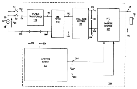
FIG. 2 describes a ballast 100 for powering at least one gas discharge
lamp 30 from a conventional alternating current (AC) voltage source 20.
Ballast
100 comprises a plurality of input connections 102,104,106, a sensing
transformer 120, an electromagnetic interference (EMI) filter 140, a full-wave
rectifier circuit 160, a capacitor C1, a detector circuit 200, power factor
correction (PFC) and inverter circuits 300, and output connections 108,110.
The plurality of input connections includes a first hot input connection
102, a second hot input connection 104, and a neutral input connection 106.
First hot input connection 102 is adapted for coupling to a hot wire 22 of AC
source 20 via a first on-off switch Sl . Second hot input connection 104 is
adapted for coupling to the hot wire 22 of AC source 20 via a second on-off
switch S2. Switches S 1 and S2 are typically implemented by conventional wall
switches having an on state and an off state. Neutral input connection 106 is
adapted for coupling to a neutral wire 24 of AC source 20. Output connections
108,110 are adapted for coupling to a lamp load that includes at least one
discharge lamp 30.
Sensing transformer 120 is coupled to first and second hot input
connections 102,104. EMI filter 140 is coupled (via terminals 142,144) to
sensing transformer 120 and to neutral input connection 106. Full-wave
rectifier 160 is coupled (via terminals 162,164) to EMI filter 140. PFC and
inverter circuits 300 are coupled (via terminals 302,304) to full-wave
rectifier
160 and capacitor Cl. Finally, PFC and inverter circuits 300 are coupled (via
output connections 108,110) to lamp 30.
Detector circuit 200 is coupled to sensing transformer 120. During
operation, detector circuit 200 provides an output voltage, VouT, having a
magnitude that is dependent on the states of switches Sl,S2. More
specifically,
when both switches Sl and S2 are in the on state, the magnitude of VouT is at
a
first level (e.g., 0 volts), causing the ballast (via PFC and inverter
circuits 300)
to operate lamp 30 at a first light level (e.g., 100% of full light output).
When
only one of the switches S 1 and S2 is in the on state, the magnitude of VouT
is at
CA 02537911 2006-02-28
a second level (e.g., 15 volts), causing the ballast to operate lamp 30 at a
second
light level (e.g., 50% of full light output).
PFC and inverter circuits 300 may be realized by any of a number of
arrangements that are well known to those skilled in the art, and thus will
not be
5 described in any further detail herein. For example, PFC and inverter
circuit
300 may be implemented using a boost converter followed by a driven series
resonant half bridge inverter. For purposes of the present invention, it is
required that PFC and inverter circuits 300 are capable of responding to the
output, Vo~T, of detector circuit 200 in the manner previously described. More
specifically, it is important that PFC and inverter circuits 300 drive lamp 30
at
the first light level (e.g., 100% of full light output) when VouT is at the
first
level (e.g., zero volts), and at the second light level (e.g., 50% of full
light
output) when Vo~T is at the second level (e.g., 15 volts).
Preferred structures for sensing transformer 120, EMI filter 140, full-
wave rectifier 160, and detector circuit 200 are now described with reference
to
FIG. 3 as follows.
Sensing transformer 120 includes first and second primary windings
122,128 and a secondary winding 134. First primary winding 122 is electrically
coupled to first hot input connection 102, and has a first polarity (as
indicated by
the dot on the left side of winding 122). Also, as described in FIG. 3, first
primary winding 122 is electrically coupled (on one end) to second primary
winding 128. Second primary winding 128 is electrically coupled to second hot
input connection 104 and is magnetically coupled to first primary winding 122;
second primary winding 128 has a second polarity (as indicated by the dot on
the right side of winding 128) that is opposite that of the first polarity.
Also, as
described in FIG. 3, second primary winding 128 is electrically coupled (on
one
end) to first primary winding 122. Secondary winding 134 is magnetically
coupled to first and second primary windings 122,128, and is electrically
coupled to detector circuit 200.
Preferably, sensing transformer 120 is realized using a toroidal core. In
order to ensure proper operation, it is important that the core have a high
permeability. A high permeability is required because of the low frequency
CA 02537911 2006-02-28
6
(e.g., 60 hertz) currents that flow through one or both primary windings
122,128
during operation of ballast 100. Preferably, each of the primary windings
122,128 is wound with 1 wire turn, and secondary winding 134 is wound with
about 500 wire turns.
EMI filter 140 may be realized by any of a number of suitable
arrangements that are well known to those skilled in the art. As an example of
a
preferred implementation, as described in FIG. 3, EMI filter 140 includes
first
and second inputs 142,144, a first inductor 146, a second inductor 152, and a
capacitor 158. First and second inductors 146,152 are magnetically coupled to
each other.
Full-wave rectifier 160 is preferably realized by a diode bridge
comprising four diodes D1,D2,D3,D4 connected in a conventional manner. A
capacitor C1 is coupled between full-wave rectifier 160 and PFC and inverter
circuits 300. Capacitor C1 is typically realized by a relatively low valued
capacitance (e.g., on the order of less than one microfarad; the preferred
value is
dependent on the number & type of lamps to be powered by the ballast).
As described in FIG. 3, detector circuit 200 preferably includes first and
second input terminals 202,204, first and second output terminals 206,208, a
comparator U1, a diode D5, a first resistor R2, a capacitor C2, a second
resistor
R3, a third resistor R4, and a fourth resistor R5. First and second input
terminals 202,204 are coupled to the secondary winding 134 of sensing
transformer 120. First input terminal 202 is also coupled to a circuit ground
60.
First and second output terminals 206,208 are coupled to PFC and inverter
circuits 300. Second output terminal 208 is also coupled to circuit ground 60.
Comparator U 1 has a non-inverting (+) input 3, an inverting (-) input 2,
and a comparator output 1. Non-inverting input 3 is coupled to a first node
210,
inverting input 2 is coupled to a second node 212, and comparator output 1 is
coupled (via a third node 214) to first output terminal 206. Comparator U 1
also
includes a DC supply input 4 and a ground terminal 11. DC supply input 4 is
coupled to a direct current (DC) voltage source (+VCC) that provides a
suitable
DC voltage, such as +15 volts, for operating comparator U1. Ground terminal
11 is coupled to circuit ground 60.
CA 02537911 2006-02-28
7
Diode DS is coupled between second input terminal 204 and (via first
node 210) the non-inverting input 3 of comparator U 1. First resistor R2 and
capacitor C2 are each coupled between non-inverting input 3 and circuit ground
60. Second resistor R3 is coupled between the DC voltage source (+V~~) and
inverting input 2. Third resistor R4 is coupled between inverting input 2 and
circuit ground 60. Fourth resistor RS is coupled between comparator output 1
and circuit ground 60.
During operation of detector circuit 200, resistors R3,R4 function as a
voltage divider that provides a low level reference voltage (e.g., on the
order of
about 100 millivolts or so) at the inverting input 2 of comparator U 1. The
voltage at the non-inverting input 3 is dependent on the voltage provided
across
input terminals 202,204 by sensing transformer 120, which, in turn, is
dependent
on the states of switches S1,S2. During operation, the voltage at the non-
inverting input 3 is compared with the reference voltage at the inverting
input 2.
When the voltage at non-inverting input 3 is less than the reference voltage,
the
voltage at comparator output 1 (and, correspondingly, VouT) will be
essentially
zero. Conversely, when the voltage at non-inverting input 3 is greater than
the
reference voltage, the voltage at comparator output 1 (and, correspondingly,
VouT) will be approximately equal to the DC supply voltage +VC~ (e.g., 15
volts).
The detailed operation of ballast 100 and detector circuit 200 is now
described with reference to FIG. 3 as follows. The four operating conditions
of
interest are: (i) S 1 and S2 off; (b) S 1 and S2 on; (c) S 1 on and S2 off;
and (d) S 1
off and S2 on. In the following description, the frequency of AC source 20 is
assumed to be 60 hertz. Additionally, unless stated otherwise, all voltages
are
understood to be with respect to circuit ground 60.
(a) When both switches S 1 and S2 are off, no power is applied to ballast
100 and lamp 30 is not illuminated.
(b) When both switches S 1 and S2 are on, Vou~~ will be at the first level
(e.g., zero volts) and lamp 30 will be illuminated at a full light level. This
occurs as follows. With both switches S 1 and S2 turned on, substantially
equal
currents will flow through first and second primary windings 122,128. Because
CA 02537911 2006-02-28
8
of the opposite polarities of primary windings 122,128, the flux that develops
from the current flowing through first primary winding 122 will be canceled by
the flux that develops from the current flowing through second primary winding
128. That is, the net flux will be approximately zero. As a result,
essentially no
voltage will develop across secondary winding 134. Correspondingly, the
voltage at second input terminal 204 of detector circuit 200 will be
essentially
zero. Within detector circuit 200, the voltage at the non-inverting input 3 of
comparator U1 will be essentially zero and, thus, less than the reference
voltage
(e.g. 0.1 volts) at the inverting input 2 of comparator U1. Conseguently, the
voltage at comparator output 1 (and, correspondingly, VouT) will be
essentially
zero. As previously described, with VouT at zero volts, PFC and inverter
circuits
300 will operate in a non-dimmed mode and power the lamp 30 at a full light
level.
(c) When switch S1 is on and switch S2 is off, VouT will be at the second
level (e.g., 15 volts) and lamp 30 will be operated at a reduced light level.
This
occurs in the following manner. With S 1 on and S2 off, a current will flow
through first primary winding 122, but no current will flow through second
primary winding 128. The flux that develops from the current flowing through
first primary winding 122 will cause a low value 60 hertz AC voltage (e.g.,
having a peak value on the order of a few volts or so) to develop across
secondary winding 134. That voltage will be applied to the second input
terminal 204 of detector circuit 200. Within detector circuit 200, the voltage
at
the non-inverting input 3 of comparator Ul will thus be greater than the small
reference voltage (e.g., 0.1 volts) at the inverting input 2 of comparator Ul.
Consequently, the voltage at comparator output 1 will go high (e.g., 15
volts).
VouT will thus be at its second level (e.g., 15 volts). As previously
described,
with VouT at its second level, PFC and inverter circuits 300 will operate in a
reduced power mode, causing lamp 30 to be illuminated at a reduced light level
(e.g., 50% of full light output).
(d) When switch Sl is off and switch S2 is on, VouT will be the same as
previously described for when S 1 is on and S2 is off (i.e., VouT will be at
the
second level and lamp 30 will be illuminated at a reduced light level). In
this
CA 02537911 2006-02-28
9
case, a current will flow through second primary winding 128, but no current
will flow through first primary winding 122. The flux that develops from the
current flowing through second primary winding 128 will cause a low value 60
hertz AC voltage to develop across secondary winding 134. That voltage will be
applied to the second input terminal 204 of detector circuit 200. Within
detector
circuit 200, the voltage at the non-inverting input 3 of comparator U1 will be
greater than the reference voltage (e.g., 0.1 volts) that is present at the
inverting
input 2 of comparator U 1. Consequently, the voltage at comparator output 1
will
go high. VouT will thus be at its second level (e.g., 15 volts). As previously
described, with VouT at its second level, PFC and inverter circuits 300 will
operate in a reduced power mode, causing lamp 30 to be illuminated at a
reduced
light level (e.g., 50% of full light output).
In this way, sensing transformer 120 and detector circuit 200 monitor the
states of switches Sl,S2, and provide a control signal to PFC and inverter
circuits 300 for selectively operating lamp 30 at two light levels.
Although the present invention has been described with reference to
certain preferred embodiments, numerous modifications and variations can be
made by those skilled in the art without departing from the novel spirit and
scope of this invention.
What is claimed is: