Note: Descriptions are shown in the official language in which they were submitted.
CA 02537974 2006-03-03
WO 2005/024379 PCT/US2004/028626
FIBER OPTIC SENSOR SYSTEM
FIELD OF THE INVENTION
The invention generally relates to fiber optic sensors, and more particularly
to
a fiber optic sensor identification system.
BACKGROUND OF THE INVENTION
Available electronic sensors measure a variety of values, such as, pH, color,
temperature, or pressure, to name a few. For systems that require a string of
electronic sensors over a long distance, e.g., twenty to thirty kilometers or
longer,
powering the electronic sensors becomes difficult. Conventionally, the
powering of
electronic sensors requires running electrical wire from a power source to
each of the
electronic sensors. However, electric wires spanning such long distances
create too
much interference and noise, thereby reducing the accuracy of the electronic
sensors.
Optical fibers have become the communication medium of choice for long
distance communication due to their excellent light transmission
characteristics over
long distances and the ability to fabricate such fibers in lengths of many
kilometers.
Further, the light being communicated can also power the sensors, thus
obviating the
need for lengthy amounts of electric wire. This is particularly important in
the
petroleum and gas industry, where strings of electronic sensors are used in
wells to
monitor down hole conditions. Powering electronic sensors electrically has
been a
problem in the petroleum and gas industry.
As a result, in the petroleum and gas industry, fiber optic sensors are used
to
obtain various down hole measurements, such as, pressure or temperature. A
string of
optical fibers within a fiber optic system is used to communicate information
from
wells being drilled, as well as from completed wells.
Conventionally, each sensor in a multi-sensor fiber optic system is calibrated
to a particular communication channel. Thus, each sensor sends data back to a
dedicated communication channel. Currently, calibration coefficients for each
communication channel, which are necessary to ensure that data from a
particular
sensor is communicated to the proper channel, are manually entered. If a
particular
channel is defective or, for whatever reason, cannot be used to receive data,
the
-1-
CA 02537974 2008-12-29
calibration coefficients for the respective sensor have to be manually re-
entered into
another channel, increasing the possibility of human error.
SUMMARY OF THE INVENTION
Accordingly, in one aspect there is provided an optic sensor system
comprising:
an optical sensor outputting an optical signal connected to a monitoring
apparatus and an identification device dedicated to the sensor, wherein the
optical
sensor is capable of returning a return optical signal, which includes a
unique identifier
from the identification device when the monitoring apparatus sends an
interrogating
optical signal to the optical sensor, wherein the interrogating optical signal
reaches the
optical sensor in a substantially unaltered waveform.
BRIEF DESCRIPTION OF THE DRAWINGS
In the accornpanying drawings, which form a part of the specification and are
to be read in conjunction therewith and in which like reference numerals are
used to
indicate like parts in the various views:
FIG. 1 is a schematic view of a fiber optic system having identification
systems constructed in accordance with an exemplary enibodiment of the
invention;
and
FIG. 2 is a schematic view of an alternate embodiment of a fiber optic system
having identification systems.
DETAILED DESCRIPTION OF THE PREFERRED EMBODIMENTS
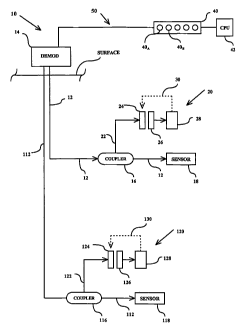
Referring to FIG. 1, a fiber optic system 10 is shown. System 10 includes a
monitoring apparatus 50 including a channel array 40 and a central processing
unit 42
in connection with an interrogator 141ocated at the surface. Preferably,
interrogator
14 is a demodulator. A first fiber 12 extends from demodulator 14 down to a
first
sensor 18. Also illustrated is a second fiber 112 extending down to a second
sensor
118. It should be appreciated that the number of fibers 12, 112 extending down
hole
-2-
CA 02537974 2006-03-03
WO 2005/024379 PCT/US2004/028626
from demodulator 14 is not fixed and is a sufficient number of fibers to allow
communication between a number of sensors 18, 118 down hole with demodulator
14.
Sensors 18, 118 are each associated with a respective, dedicated
identification
system 20, 120. Identification system 20 includes a coupler 16, a shunt line
22, a
modulating device 24, a power converting device 26, and a high temperature
integrated circuit 28. Identification system 120 similarly includes a coupler
116, a
shunt line 122, a modulating device 124, a power converting device 126, and a
high
temperature integrated circuit 128.
Monitoring apparatus 50 may be a standard stationary monitoring apparatus,
or it may be a portable monitoring apparatus that is transported from well to
well for
the purpose of obtaining data from each respective well. For example, a
portable
monitoring apparatus 50 may be coupled with a first well, at which relevant
data from
the well, taken and reported by sensors 18, 118, is obtained. Then, the
portable
monitoring apparatus 50 may be decoupled from the first well, moved to a
second
well, and coupled with the second well to obtain like information.
After monitoring apparatus 50 has been coupled with a well, it is important to
ascertain which sensors are associated with which channel in channel array 40.
As
shown, two channels 40A and 40B are denoted. To ascertain which sensor 18, 118
is
associated with which fiber 12, 112, a signal is sent from demodulator 14 down
fiber
12. The light signal, travels through fiber 12 to coupler 16, where a majority
of the
light continues along fiber 12 to sensor 18. A portion of the light, such as
about ten
percent (10%), is shunted off onto fiber optic shunt line 22 toward modulating
device
24.
Modulating device 24 may modulate through any suitable mechanism, such as
through electro-optical or microelectromechanical (MEMS) means. Modulating
device 24 causes periodic intensity variations in the light reflected back to
demodulator 14 through coupler 16 in response to the light sent from
demodulator 14
to identification system 20. In other words, the intensity variations only
occur when
individual sensor 18 is addressed. The modulation occurs as a result of
changing the
properties of the optical path. This can be accomplished by inserting a
reflector in the
path with a MEMS device or changing the polarization with an LCD device.
The light transmitted through shunt line 22 is transmitted through modulating
device 24 and converted into electrical energy by power converting device 26.
-3-
CA 02537974 2006-03-03
WO 2005/024379 PCT/US2004/028626
Alternatively, the light transmitted through shunt line 22 may be transmitted
directly
to power converting device 26 for conversion into electrical energy. A
suitable power
converting device 26 may be a photocell. Power converting device 26 may
include an
anti-reflective coating which provides a minimum and constant amount of
reflection
to minimize interference with fiber optic sensor 18.
The now converted electric energy powers integrated circuit 28. Information
identifying the particular sensor 18 to which identification system 20 is
coupled is
stored on integrated circuit 28. Integrated circuit 28 may be a standard high
temperature integrated circuit such as those manufactured by Honeywell and
rated to
200 C for a ten year mean time before failure (MTBF). Alternatively,
integrated
circuit 28 may include one of various more exotic constructions, such as
sapphire or
diamond, which are rated for higher than 200 C for a ten year MTBF.
The electrical energy, which comes from power converting device 26 to
integrated circuit 28, provides power to integrated circuit 28 to allow it to
send the
identifying information back to the surface. In response to the electrical
energy,
integrated circuit 28 sends a modulating response 30 back to modulating device
24.
Modulating response 30 may be as simple as a digital identification number
corresponding to relevant sensor 18 or as complex as all the calibration data
for
relevant sensor 18. Modulating device 24 forwards modulating response 30 back
through coupler 16 and up fiber 12 to demodulator 14 on the surface. The
identifying
information is used to verify that sensor 18 is associated with fiber 12 and
is
calibrated to a particular channel, such as channel 40A. A similar exercise is
then
accomplished with fiber 112 to verify that sensor 118 is associated with fiber
112.
In operation, a light signal is transmitted through fiber 12 by monitoring
apparatus 14 to coupler 16 corresponding with a particular sensor 18 and its
respective identification system 20. The signal is for only a specific sensor,
and thus
only its respective identification system 20 will be enabled to respond. A
portion of
the light is shunted away from fiber 12 leading to sensor 18 and onto optical
fiber
shunt line 22. The shunted light passes through modulating device 24, such as
a
liquid crystal display, which then transmits the light to power conversion
device 26,
such as a photocell. Photocell 26 transforms the light energy into electrical
energy
and sends the electrical energy in pulses toward the high temperature
integrated
circuit 28.
-4-
CA 02537974 2006-03-03
WO 2005/024379 PCT/US2004/028626
Now powered by the electrical energy, and in response to the pulsed signal
provided by photocel126, integrated circuit 28 sends a modulating response 30
to
modulating device 24. Modulating response 30 is determined by the digital
information contained in integrated circuit 28. Integrated circuit 28 does not
send any
information until the proper sequence of pulses is first received from
photocel126.
The pulse sequence is a trigger or command for the sensor circuit to send one
or more
packets of information. Modulating response 30 is then transmitted back up to
the
surface.
Alternatively, modulating device 24 may be pre-set to reflect the shunted
light
at a particular intensity, which intensity correlates to a particular sensor
18. For
example, modulating device 24 may be a digital micromirror device (DMD), such
as
those available from Texas Instruments. While most DMDs are dynamically
controlled, i.e., the individual micromirrors in the array are toggled in real
time to
drive the modulation of the optical beam, a DMD may also be passive. In this
case,
the individual micromirrors are set into a particular configuration which is
not altered
thereafter. Central processing unit 42 can be pre-programmed to recognize the
signature generated by the modulation caused by a particular DMD to identify a
particular sensor. For example, central processing unit 42 may contain memory
that
stores a database of signatures and corresponding sensors as well as
calibration data
related to those sensors. By comparing the detected signal to the signatures
in the
database, sensor 18 may be identified.
Additionally, the digital information contained in integrated circuit 28 can
also
be stored in central processing unit 42. When the information identifying the
sensor
is stored in the central processing unit 42 or the monitoring device 50,
dedicated
channels 40A, 40B may be omitted. The measurement readings from sensors 18,
118
are continually coupled with or are associated with the identifying
information,
thereby associating the measurements to the sensor without the need for a
dedicated
channel.
In another embodiment, shown in FIG. 2, a fiber optic system 210 is includes
a monitoring apparatus 250 that includes a channel array 240 and a central
processing
unit 242 at the surface, similar to channel array 40 and central processing
unit 42
discussed above with respect to FIG. 1.
-5-
CA 02537974 2006-03-03
WO 2005/024379 PCT/US2004/028626
Monitoring apparatus 250 also includes at the surface an interrogator 214.
Preferably, interrogator 214 is an optical frequency domain reflectometer
(hereinafter,
"OFDR"). Such devices are known in the art, and OFDRs typically utilize swept-
wavelength interferometry to interrogate systems and/or devices. OFDR 214 may
be
any OFDR known in the art, such as those available from Luna Technologies Inc.
of
Blacksburg, VA. OFDR 214 includes at least a light source 244 and a detector
246.
Although shown in FIG. 2 as separate components, alternatively, OFDR 214 may
also
incorporate channel array 240 and/or central processing unit 242 within a
single unit
(not shown).
A first fiber 212 connects OFDR 214 to a first sensor 218. Similarly, a second
fiber 312 connects OFDR 214 to a second sensor 318. More sensors may be
utilized
as desired, depending upon the well system to be monitored. Associated with
each
sensor 218, 318 is a dedicated identification device 220, 320, respectively.
For clarity
of description, the arrangement of system 210 with respect to sensor 218 is
described;
the other sensors within system 210 are arranged in a similar manner.
Identification device 220 is preferably a fiber Bragg grating (FBG), although
the use of any reflective medium capable of causing intensity or frequency
variations
or phase shift within a light beam is appropriate for use with the present
invention.
Identification device 220 is preferably placed in series with sensor 218 on
fiber 212.
As would be apparent to those skilled in the relevant art, identification
device 220
may be a separate FBG that is optically coupled with fibers 212.
Alternatively,
identification device 220 may also be written directly into fiber 212, or
incorporated
into sensor 218. FBGs that modulate or reflect light to encode signals are
known in
the art.
Encoded into identification device 220 is information related to their
respective associated sensor 218 such as a serial number, calibration data, or
the like.
Preferably, a binary "bit" is written in a specific spatial location in fiber
212. In other
words, at a given location along the length of fiber 212, a value of one or
zero is
encoded, where "one" is the presence of a grating pattern or other reflective
device
and "zero" is the absence of a grating pattern or other reflective device. A
series of
bits at pre-determined locations within fiber 212 contain all of the desired
information, such as numbers in a serial code or a calibration coefficient.
Each
encoded location could be specified to be, for the purposes of example only, 1
cm
-6-
CA 02537974 2006-03-03
WO 2005/024379 PCT/US2004/028626
apart starting at a specific point in fiber 212. A series of bits could
correspond to a
particular digit in the sensor serial number or calibration coefficient. Any
known
binary coding scheme could be employed.
In operation, OFDR 214 interrogates sensor 218 by passing an optical signal
through identification device 220 as the light travels to and from sensor 218.
Both
sensor 218 and identification device 220 alter the optical beam to encode data
therewithin. The signal is then reflected back to OFDR 214, where the signal
is
detected. In addition to the information gathered from sensor 218, OFDR 214
detects
the encoded identification information reflected from identification device
220. The
information is then transmitted to central processing unit 242. Central
processing unit
242 is programmed with the predetermined bit spacing and format, and the
necessary
fiber sensor identification or calibration information can then be
extrapolated. Sensor
218 may then be identified, calibrated, and assigned to a specific channel
240A within
channel array 240. A similar process is performed for sensor 318 using
identification
device 320 to assign sensor to a channe1240B, as well as any other sensors
included
with system 210. Alternatively, as the encoded information from identification
device
220, 320 is transmitted with each interrogation, central processing unit 242
may be
programmed to determine the sensor of origin of the signal with each
interrogation.
In such a case, sensor 218 would not be assigned to a dedicated channel.
Alternatively, identification device 220 may be the optical fiber lead to
sensor
218. As is known in the art, Rayleigh scattering, the scattering of light by
the
particles of the material through which the light is transmitted, occurs in
optical fiber
transmissions. When sensor 218 is manufactured, the unique Rayleigh scattering
profile of the lead is scanned with an OFDR. This Rayleigh scattering profile,
which
remains fixed throughout the usable life of sensor 218, is recorded and stored
in a
database in central processing unit 240. Sensor 218 is deployed down hole by
splicing the lead onto fiber 212 or coupling the lead thereto using a
mechanical
coupler. After sensor 218 is deployed down hole, OFDR 214 interrogates sensor
218
and compares the received Rayleigh scattering profile with the database,
thereby
identifying the scanned sensor as sensor 218.
Yet another manner in which the lead to sensor 218 may be used as
identification device 220 is to intentionally vary the length of the leads for
all sensors
in system 210 in a known fashion. In a typical multi-sensor system, care is
taken to
-7-
CA 02537974 2006-03-03
WO 2005/024379 PCT/US2004/028626
splice all leads the same length and to ensure invisibility of the splice.
However, for
use as identification device 220, the splice is intentionally made visible to
the
interrogation beam. Using sensor 218 as a reference reflector, the distance
between
the splice and sensor 218 is measured. This measurement is then compared with
a
database of sensor lead lengths stored in central processing unit 242 in order
to
identify the scanned sensor as sensor 218.
Another alternative for identification device 220 is a spectral filter. OFDR
214 preferably employs a tunable laser as the light source. This laser cycles
through
the available channels at specified increments. A typical OFDR utilizes
hundreds of
channels. Identification device 220 can remove a pre-determined portion of the
channel spectrum, thereby providing a signature to identify sensor 218.
While it is apparent that the illustrative embodiments of the invention
disclosed herein fulfill the objectives of the present invention, it is
appreciated that
numerous modifications and other embodiments may be devised by those skilled
in
the art. Additionally, feature(s) and/or element(s) from any embodiment may be
used
singly or in combination with other embodiment(s). Therefore, it will be
understood
that the appended claims are intended to cover all such modifications and
embodiments, which would come within the spirit and scope of the present
invention.
-8-