Note: Descriptions are shown in the official language in which they were submitted.
CA 02538345 2006-03-08
WO 2005/027448 PCT/US2004/029867
CHANNEL BONDING OF A PLURALITY OF MULTI-GIGABIT
TRANSCEIVERS
BACKGROUND OF THE INVENTION
TECHNICAL FIELD OF THE INVENTION
This invention relates generally to general-purpose
integrated circuits and more particularly to integrated
circuits having a plurality of serial transceivers.
DESCRIPTION OF RELATED ART
As is known, integrated circuits (ICs) may be fabricated
using a variety of technologies (e. g., CMOS, gallium
arsenide, silicon germanium, bi-polar, etc.) to provide an
endless list of electronic circuits. For example,
microprocessors, read only memory (ROM), static random
access memory (SRAM), dynamic random access memory (DRAM),
field programmable gate arrays (FPGA), and digital signal
processors (DSP) are typically fabricated using CMOS
technology and provide vast programmable electronic
2o circuits and/or data storage.
As the amount of data processed by such ICs increases and
the time to process such data decreases, getting the data
on to and off of the chip in sufficient amounts and in a
timely manner presents an ever increasing IC design
challenge. One common solution to this problem is to
increase the width of the input and output interfaces of
the IC. For instance, the data may be provided in parallel
in 32 bit data words, 64 bit data words, etc. While this
technique meets its objective, it requires the IC to a
large number of pins to accommodate the large parallel
inputs and outputs, which increases the IC package size,
increases die size, adds cost, and makes IC and printed
circuit board (PCB) layouts more difficult.
Another solution is to include high-speed serial interfaces
on the IC. As is known, a high-speed serial interface
transmits and receives a serial stream of data, thus
requiring only one IC pin for the transmit path and one IC
pin for the receive path. As is further known, a high
speed interface converts received serial data into parallel
4o data to correspond to the internal bus size of the IC. In
1
CA 02538345 2006-03-08
WO 2005/027448 PCT/US2004/029867
addition, a high.-speed serial interface, or transceiver,
converts transmit parallel data into transmit serial data.
5nrhen such high-speed serial interfaces are implemented
using CMOS technology, the rate of the serial data is
somewhat limited. For example, a 3.125 Gigabit-per-second
(Gbps) serial data rate is about the maximum rate for 0.18
micron CMOS technology.
To achieve data rates above a technology limitation (e. g.,
the 3.125 Gbps for 0.18 micron CMOS), several serial
so channels may be operated in parallel, which is referred to
as channel bonding. For example, to achieve a 12.5 Gbps
data rate, four 3.125 Gbps transceivers may be bonded
together (i.e., 4*3.125 - 12.5). In this example, each
transceiver processes 1/4t'' of the data, which is done at
the same time as the other transceivers are processing
their respective fourths of the data.
The technical challenge with channel bonding is to insure
that each transceiver stays in step with all of the other
transceivers, such that the ordering of the data is not
lost during the parallel processing. For instance, in the
four transceiver example, a first transceiver processes the
first of every four bits of the input or output serial
data, a second transceiver processes the second of every
four bits of the input or output serial data, a third
transceiver processes the third of every four bits of the
input or output serial data, and a fourth transceiver
processes the fourth of every four bits of the input or
output serial data. If this ordering is lost, even
temporarily, the received or transmitted data will be
3o corrupted.
Due to channel bonding set-up latencies (i.e., the
processing time to recognize initiation of channel bonding,
to adjust memoxy access timing, and to allocate
responsibilities to the transceivers), the number of
3s transceivers that can be bonded together are limited.
Typically, only about four 3.125 Gbps transceivers can be
bonded together due to set-up latencies. As the dies size
increases, the spacing of the transceivers may also
increase, which adds to the set-up latencies. Further,
2
CA 02538345 2006-03-08
WO 2005/027448 PCT/US2004/029867
consumer demands for even higher data rates (e. g., ~0 Gbps)
are increasing.
Therefore, a need exists for a technique of bonding a
significant number of channels (i.e., high-speed serial
transceivers) to achieve high data rates without limitation
due to set-up latencies.
BRIEF SUN.~lARY OF THE INVENTTON
The channel bonding of a plurality of multi-gigabit
so transceivers of the present invention substantially meets
these needs and others. In one embodiment, a method for
channel bonding a plurality of mufti-gigabit transceivers
begins when a master transceiver of the plurality of multi
gigabit transceivers receives a channel bonding sequence
(i.e., an indication for channel bonding, which includes
the desired data rate, the number of channels being
bonding, and channel assignments). The process continues
with the master transceiver generating a channel bonding
request (e. g., specific slave channel bonding
responsibilities) in response to the channel bonding
sequence. The process continues with the master
transceiver transmitting the channel bonding request and
channel bonding configuration information (e.g., number of
slaves, propagation delays, arid clock correction
information) to slave transceivers of the plurality of
mufti-gigabit transceivers.
The process continues with each of the slave transceivers
receiving the channel bonding sequence and, at the same or
a different time, receiving the channel bonding request anal
3o the channel bonding configuration information. The process
continues as each of the slave transceivers processes the
channel bonding request and the channel bonding sequence in
accordance with the channel bonding configuration
information to determine individual slave channel bonding
start information. The process continues as the master
transceiver processes the channel bonding sequence in
accordance with the channel bonding configuration
information and the channel bonding request to determine
master channel bonding start information.
3
CA 02538345 2006-03-08
WO 2005/027448 PCT/US2004/029867
The process continues by commencing channel bond writing of
respective data to and reading of the respective data from
corresponding buffers by the master transceiver and the
slave transceivers in accordance with the individual slave
channel bonding start information and the master channel
bonding start information. With such a method, propagation
delays of processing the channel bonding set-up are
accounted for and, as such, can be factored into setting up
a wide channel (e. g., a large number of transceivers bonded
1o together).
In another embodiment, a method for channel bonding by a
multi-gigabit transceiver begins by determining whether the
mufti-gigabit transceiver is a master transceiver or a
slave transceiver. When the mufti-gigabit transceiver is
~5 the slave transceiver, the process continues by detecting a
channel bonding sequence at a given time to produce a
detected channel bond sequence. The slave process
continues by delaying the detected channel bonding sequence
for a predetermined period of time to produce a delayed
2o channel bonding sequence. The slave process continues by
receiving a channel bonding request at a second given time.
The slave process continues by determining whether the
receiving of channel bonding request and the delayed
channel bonding sequence are within a time window.
25 When the receiving of channel bonding request and the
delayed channel bonding sequence are within the time
window, the slave process continues by aligning data with
respect to data alignment of the master transceiver to
produce aligned data. The slave process continues by
3o synchronizing the aligned data with data of the master
transceiver. With such a method, propagation delays of
processing the channel bonding set-up are accounted for
and, as such, can be factored into setting up a wide
channel (e. g., a large number of transceivers bonded
35 together).
An embodiment of a channel bonding module for a multi-
gigabit transceiver includes a channel bonding sequence
comparator, a pointer generation module, and a channel
bonding processing module. The channel bonding sequence
4o comparator is operably coupled to a buffer of the multi-
4
CA 02538345 2006-03-08
WO 2005/027448 PCT/US2004/029867
gigabit transceiver that temporarily stores received
parallel data. As coupled, the channel bonding sequence
comparator compares data blocks (e.g., data word lines of
the buffer) of the received parallel data with a channel
bonding sequence. When a current data block of the data
blocks of the received parallel data substantially matches
the channel bonding sequence, the channel bonding sequence
comparator generates a channel bonding sequence detect
signal. The pointer generation module is operably coupled
to generate a read pointer and a write pointer for reading
to and writing from the buffer.
The channel bonding processing module is operably coupled
to: generate a channel bonding sequence address based on
the write pointer and the channel bonding sequence detect
i5 signal; generate a channel bonding start address based on
the channel bonding sequence address and channel bonding
configuration information; generate a channel bonding start
indication based on the channel bonding configuration
information; and provide the channel bonding start address
2o arid the channel bonding start indication to the pointer
generation module~such that, at commencement of channel
bonding, the write pointer corresponds to the channel
bonding start address. With. such a module, propagation
delays of processing the channel bonding set-up are
25 accounted for and, as such, can be factored into setting up
a wide channel ~(e.g., a large number of transceivers bonded
together).
BRIEF DESCRIPTION OF THE SEVERAL VIEWS OF THE DRAWINGS
3o Figure 1 is a schematic block diagram of a programmable
logic device in accordance with the present invention;
Figure 2 is a schematic block diagram of a programmable
multi-gigabit transceiver in accordance with the present
invention;
35 Figure 3 is a schematic block diagram of a programmable
receive physical coding sublayer module in accordance with
the present invention;
Figure 4 is an illustrative of channel bonding in
accordance with the present invention;
5
CA 02538345 2006-03-08
WO 2005/027448 PCT/US2004/029867
Figure 5 is a timing diagram of the illustrative channel
bonding of Figure 4;
Figure 6 is a schematic block diagram of one of a plurality
of channel bonding configurations in accordance with the
present invention;
Figure 7 is a schematic block diagram of another one of the
plurality of channel bonding configurations in accordance
with the present invention;
Figure 8 is a schematic block diagram of a channel bonding
1o module in accordance with the present invention;
Figure 9 is a logic diagram of a method for channel bonding
a plurality of multi-gigabit transceivers in accordance
with the present invention;
Figure 10 is a logic diagram of the slave processing of the
logic diagram of Figure 9; and
Figure 11 is a logic diagram of a method for channel
bonding by a multi-gigabit transceiver in accordance with
the present invention.
DETAILED DESCRIPTION OF THE INVENTION
Figure 1 is a schematic block diagram of a programmable
logic device 10 that includes programmable logic fabric 12,
a plurality of programmable multi-gigabit transceivers
(PMGT) 14-28 and a control module 30. The programmable
logic device 10 may be a programmable logic array device, a
programmable array logic device, an erasable programmable
logic device, and/or a field programmable gate array
(FPGA) . U~h.en the programmable logic device 10 is a field
programmable gate array (FPGA), the programmable logic
3o fabric 12 may be implemented as a symmetric array
configuration, a row-based configuration, a sea-of-gates
configuration, and/or a hierarchical programmable logic
device configuration. The programmable logic fabric 12 may
further include at least one dedicated fixed processor,
such as a microprocessor core, to further facilitate the
programmable flexibility offered by a programmable logic
device 10.
The control module 30 may be contained within the
programmable logic fabric 12 or it may be a separate
4o module. In either implementation, the control module 30
6
CA 02538345 2006-03-08
WO 2005/027448 PCT/US2004/029867
generates the control signals to program each of the
transmit and receive sections of the programmable multi-
gigabit transceivers 14-28. In general, each of the
programmable mufti-gigabit transceivers 14-28 performs a
serial-to-parallel conversion on received data and performs
a parallel-to-serial conversion on transmit data. The
parallel data may be 8-bits, 16-bits, 32-bits, 64-bits, et
cetera wide. Typically, the serial data will be a 1-bit
stream of data that may be a binary level signal, multi-
level signal, etc. Further, two or more programmable
mufti-gigabit transceivers may be bonded together to
provide greater transmitting speeds. For example, if
mufti-gigabit transceivers 14, 16 and 18 are transceiving
data at 3.125 gigabits-per-second, the transceivers 14-18
25 may be bonded together such that the effective serial rate
is 3 times 3.125 gigabits-per-second. Channel bonding will
be described in greater detail with reference to Figures 3
- 11.
Each of the programmable mufti-gigabit transceivers 14-28
2o may be individually programmed to conform to separate
standards. In addition, the transmit path and receive path
of each mufti-gigabit transceiver 14-28 may be separately
programmed such that the transmit path of a transceiver is
supporting one standard while the receive path of the same
25 transceiver is supporting a different standard. Further,
the serial rates of the transmit path and receive path may
be programmed from 1 gigabit-per-second to tens of
gigabits-per-second. The size of the parallel data in the
transmit and receive sections, or paths, is also
3o programmable and may vary from 8-bits, 16-bits, 32-bits,
64-bits, et cetera.
Figure 2 illustrates a schematic block diagram of a
representative one of the programmable mufti-gigabit
transceivers 14-28. In this embodiment, the programmable
35 mufti-gigabit transceiver 14-28 includes a transmit section
70, a receive section 72, a control module 35 and a
programmable interface 36. The transmit section 70
includes a programmable transmit PMA module 38 and a
programmable transmit PCS module 42. The receive section
7
CA 02538345 2006-03-08
WO 2005/027448 PCT/US2004/029867
72 includes a programmable receive PNlA module 40 and a
programmable receive PCS module 44.
In operation, the programmable logic fabric 12 provides
transmit data words 46, which may be 2 bytes, 4 bytes, 8
bytes, etc. in width, to the programmable transmit PCS
module 42 via the programmable interface 36. The
programmable transmit PCS module 42 converts the transmit
data words 46 into transmit parallel data 48, which may be
8, 16, 32, 64, etc. bits in width. The programmable
1o transmit PMA module 38 converts the transmit parallel data
into transmit serial data 50.
The programmable receive PMA module 40 is operably coupled
to convert receive serial data 52 into receive parallel
data 54, which may be 8, 16, 32, 64, etc. bits in width.
The programmable receive PCS module 44, which will be
described in greater detail with reference to Figure 3,
converts the receive parallel data 54 into receive data
words 56, which may be 2 bytes, 4 bytes, 8 bytes, etc. in
width. The programmable receive PCS module 44 provides the
2o receive data words 56 to the programmable logic fabric 12
via the programmable interface 36.
In this embodiment, the control module 35 programs the
transmit section 70 and the receive section 72 via transmit
setting 74 and receive setting 76, respectively. The
control module 35 also programs the programmable interface
36 via the logic interface setting 58. Accordingly, the
control module 35 may program the receiver section 72 to
function in accordance with one standard while programming
the transmit section 70 in accordance with another standard
3o and to participate in channel bonding. Further, the logic
interface setting 58 may indicate that the transmit data
words 46 are received from the programmable logic fabric 12
at a different rate than the receive data words 56 are
provided to the programmable logic fabric 12. As one of
average skill in the art will appreciate, the programmable
interface 36 may include a transmit buffer and a receive
buffer, and/or an elastic store buffer to facilitate the
providing and receiving of the data words 56 and 46 to-and-
from the programmable logic fabric 12.
8
CA 02538345 2006-03-08
WO 2005/027448 PCT/US2004/029867
Figure 3 is a schematic block diagram of a programmable
receive PCS module 44 that includes a programmable data
alignment module 80, a programmable descramble and decode
module 82, a programmable storage module 84, and a
programmable decode and verify module 86. The programmable
storage module 84 includes a channel bonding module 90, an
elastic storage buffer 88 and a multiplexer 92.
Tn operation, the programmable data alignment module 170
receives the receive parallel data 54. Based on settings
76, the programmable data alignment module 80 may pass the
receive parallel data 54 to the programmable descramble and
decode module 82 without processing, may validate the
receive parallel data prior to programmable descramble and
decode module 82, and/or synchronize the validated data
prior to providing it to the programmable descramble and
decode module 82.
The programmable descramble and decode module 82 receives
the output of multiplexer 184 and, based on setting 76,
either passes the data unprocessed to the programmable
2o storage module 84, descrambles the data prior to providing
it to the programmable storage module 84, and/or decodes
the data prior to providing it to the programmable storage
module 84.
The programmable storage module 84 may buffer the data it
receives from the programmable descramble and decode module
82 via the elastic store buffer 84 to facilitate channel
bonding or pass the data directly to multiplexer 92. The
channel bonding module 90, which will be discussed in
greater detail with reference to Figures 4 -11, enables the
3o receiver of one programmable mufti-gigabit transceiver to
be linked or bonded with another receiver within another
mufti-gigabit transceiver to increase the effective serial
data rate.
The programmable decode and verify module 86 receives the
output of multiplexer 92 and passes it directly as the
receive data word 56 in accordance with setting 76,
processes the data via a cyclic redundancy check, and/or
further decodes it to produce the receive data word 56.
Figure 4 is an illustrative of channel bonding of three
4o channels. In this example, PMGT 14 has been designated as
9
CA 02538345 2006-03-08
WO 2005/027448 PCT/US2004/029867
the master transceiver, while PMGTs 16 and 18 have been
designated as slave transceivers. Typically, the user of
the programmable logic device 10, or the user of an IC that
includes a plurality of multi-gigabit transceivers, makes
the master/slave designations. Alternatively, one of the
transceivers may be selected as the master via a default
mechanism. As another alternative, the master transceiver
may be dynamically established upon channel bonding
initiation.
1o As shown, MGT 14 receives TX data 1 via a transmission
line, MGT 16 receives TX data 2 via a separate transmission
line, and MGT 18 receives TX data 3 via yet another
separate transmission line. In this example, the transmit
data (TX data 1, 2, and 3) is a serial data stream that
represents four byte data words. For instance, a first
data word of TX data 1 includes four bytes (A1, B1, C1, and
a first data word of TX data 2 includes four bytes (A~,
B2, C2, and DZ) , and a first data word of TX data 3 includes
four bytes (A3, B~, C3, arid D3) . As one of average skill in
2o the art will appreciate, the data word size may correspond
to a word line of the buffer 88, a multiple thereof, and/or
to the bus width of the programmable logic device.
Tn this example, due to differences in the transmission
lines (e.g., differing transmission line effects), each of
the MGTs 14 - 18 receives, stores, and processes their
respective data at slightly different times. In addition,
due to slight differences in clock speeds of the MGTs, they
each store and process their respective data from the
elastic storage buffer 88 at slightly different rates.
3o This is illustrated in that the first bytes of each of the
first data words of the TX data 1, 2, and 3 (e.g., A1, A2,
and A3) are placed on to their respective transmission lines
in synch. However, as shown at the contents of the
respective elastic storage buffers 88, the byte alignment
of the data has shifted. For instance, MGT 16 is the first
of the three transceivers to receive, store, and process
the first byte of the first data word of TX data 2 (e. g.,
Aa) . But does so in a shifted position with respect to the
originally transmitted data (e. g., in byte position three
as opposed to byte position one).
CA 02538345 2006-03-08
WO 2005/027448 PCT/US2004/029867
MGT 14 is the next MGT to receive, store, and process the
first byte of the first data word of its corresponding TX
data, but does so three bytes later than MGT 16 received
its corresponding first byte of the first data word. As
s such, due to the different transmission line effects and
processing speeds, MGT 14 is processing its first byte of
i is f i rs t data word on a di f f erent data word 1 ine than MGT
16'. MGT 18 is the last MGT to process its first byte of
its first data word.
1o As long as the TX data is serial nonbonded data 102, which
corresponds to the first two data word lines of the TX data
1, 2, and 3 in this example, the differences in processing
time and transmission line effects do not impact the
performance of the MGTs since they are each processing
15 independent data. However, when the MGTs are to be channel
bonded, these differences need to be accounted for and
corrected.
As shown, the third data word line of each TX data includes
a channel bonding sequence, which is represented by a four
2o byte word (X, X, X, X). The channel bonding sequence
includes channel bonding set up information, which includes
one or more of, number of channels, physical sequence
(i.e., which channel supports which bytes of the TX data),
the byte width, channel bonding initiation. The channel
25 bonding sequence may further identify the master
transceiver. As shown, the channel bonding sequence 104 is
synchronously transmitted within the TX data 1, 2, and 3,
but is received, stored, and processed at slightly
different times by each of the MGTs. As is further shown,
3o the TX data transmissions pause for a specific period of
time before transmitted serial bonded data 106. The
duration of the pause depends on the channel bonding
configuration. During the pause, the TX data 1, 2, and 3
may be stopped, or continued with null, don' t care data or
35 repeated transmission of the beginning data word line of
the serial bonded data 106.
With MGT 14 as the master, when it detects the channel
bonding sequence, it generates a channel bonding request
(CBR) 100 and channel bonding configuration information
(CBCI) 108, which it provides to slaves 1 and 2 (i.e., MGT
11
CA 02538345 2006-03-08
WO 2005/027448 PCT/US2004/029867
16 and MGT 18). Note that, depending on the channel
bonding configuration, the master may provide the CBR. 100
and CBCI 108 to each slave directly or indirectly through
intervening slaves. The channel bonding request 100 is an
indication to the slaves that a channel bond is being set
up and provides a timing benchmark for the channel bond set
up. The channel bonding configuration information 108
includes the number of slaves in the channel bond, the
propagation delays of the slaves with respect to the
1o master, and clock correction information. The clock
correction information includes pointer separation
information, an address offset, and an adjust enable
signal.
To establish channel bonding, the master processes the
channel bonding sequence to determine the channel bonding
start. The slaves process the channel bonding sequence
along with the channel bonding request 100 and the channel
bonding configuration information 108 to identify the
channel bonding start, and to align and synchronize the
2o processing of its data with the processing of the data by
the master. As shown, the first data word that can be
bonded begins with a four byte word (W, X, Y, and z) for
each TX data 1, 2, and 3. Due to the transmission line
effects and/or process speed, the master processes its data
words shifted by one byte. This establishes the byte
alignment for all of the slaves, which they must adjust to.
Further, the processing speed at which the master reads and
writes data into its corresponding buffer 88 provides the
reading and writing rate to which the slaves must
3o synchronize. In addition, the master determines, based on
the maximum propagation delay of the channel bonding
configuration, that the first data word that can be bonded
is data word (W, X, Y, Z). This information may also be
provided to the slaves.
While the channel bond is being established, the master and
slaves are still independently operating. As such, until
the channel bonding commences, the slaves continue to store
data at its independent rate with its independent byte
offset. However, upon processing the channel bonding
4o sequence, the channel bonding request, and the channel
12
CA 02538345 2006-03-08
WO 2005/027448 PCT/US2004/029867
bonding configuration information, each of the slaves knows
when the channel bonding will begin, the first data word
line of the bonded data, and the byte position of the data
word line.
As shown, slave 1, which, in time, is ahead of the master,
receives and processes the first data word that can be
bonded prior to the master, thus it stores the data as it
receives it. However, when the channel bonding begins, the
first data word, or a portion thereof, is again stored in
so its buffer. As illustrated, slave 1 repeats the storing of
bytes W, X and Y to obtain the alignment and
synchronization with the master's storing of these bytes.
As is also shown, slave 2 is trailing, in time, the
master's storing of data words. Thus, at the commencement
of the channel bonding, slave 2 jumps ahead to the
appropriate data word (W, X, Y, Z), thus omitting the
storing of bytes U and V of the preceding data word, to
obtain alignment and synchronization with the master.
With the slaves aligned and synchronized with the master,
2o the resulting data of the corresponding buffers 88 of each
of the MGTs is channel bonded. By including the
propagation delays of the MGTS in the set up process, the
latencies of channel bonding set up can be accounted for
and factored into the channel bond establishment. As such,
the number of transceivers that can be bonded together is
limited only by the number of transceivers on an integrated
circuit. Further, the slaves may be coupled to the master
in a wide variety of configurations.
Figure 5 is a timing diagram of the illustrative channel
3o bonding of Figure 4. In this illustrative example, the
functioning of the master and the slaves of Figure 4 to
establish a channel bond are separately graphed in time.
As shown, the master MGT detects the channel bonding
sequence (CBS) at a given time, which triggers the master
to generate the channel bonding request (CBR), to generate
the channel bonding configuration information (CBCI), to
determine a wait period based on the maximum propagation
delay before commencing channel bonding, and to determine
its channel bonding start address based on the wait period
4o and the detection of the CBS.
13
CA 02538345 2006-03-08
WO 2005/027448 PCT/US2004/029867
As part of detecting the channel bonding sequence (CBS),
the master determines the address of its buffer at which
the CBS is stored to produce a CBS address. The master
interprets the CBS to determine the number of slaves in the
channel bond. and to determine the channel bonding
configuration. As will be discussed with reference to
Figures 6 and 7 , there are a variety of ways in which the
slaves may be coupled to the master to accomplish channel
bonding.
1o The master knows its processing time to prepare the channel
bonding request (CBR), the propagation delays to transmit
the CBR to each of the slaves, and the processing time of
each slave to process the CBR, the channel bonding
sequence, and the channel bonding configuration information
to be ready for channel bonding commencement. The maximum
propagation delay for the master thus includes it
processing time to generate the CBR and the longest delay
of the slaves to be ready for channel bonding. In this
example, slave 2 has the longest delay. Note that there is
2o some additional time added to the wait period for the
master after slave 2 is ready to account for process
variations, temperature variations, and/or to provide some
tolerance.
The master also generates the channel bonding configuration
information (CBCI) that is subsequently provided to the
slaves. V~hile this example illustrates the master
generating the CBCI after completion of generating the
channel bonding request (CBR), the master may generate the
CBCI any time after it detects the channel bonding sequence
(CBS) .
The master then generates its channel bonding start address
based it processing time of the CBR, the maximum
propagation delay, its processing rate, and the CBS
address. For example, if the CBS address is address 100,
the memory includes a four byte data word line, a word line
of data can be processed in 1 microsecond, its processing
time of the CBR is 10 microseconds, and the maximum
propagation delay is 25 microseconds, at total of 35
microseconds pass from the detection of the CBS until the
4o system is ready for channel bonding. During those 35
14
CA 02538345 2006-03-08
WO 2005/027448 PCT/US2004/029867
microseconds, 35 word lines of data will be received, thus
the write pointer to the buffer will advance 35 addresses
from the CBS address. Thus, the channel bonding start
address is 136 (e. g., 100 + 35 + 1), which is the next
address in time.
The time line for slave 1 begins when it detects the
channel bonding sequence (CBS). As shown, slave 1 detects
the CBS prior to the master detecting the CBS, which was
also illustrated in Figure 4. To account for the
1o processing delays of the master in preparing the channel
bonding request (CBR) and the propagation delays in
receiving the CBR, slave 1 effectively delays the detection
of the CBS for a specific period of time to produce a
delayed CBS. Upon detecting the CBS, slave 1 begins to
z5 look for the CBR from the master or for the delayed CBS.
In this example, since slave 1 is ahead of the master, the
delayed CBS occurs, in time, before it receives the CBR.
As such, at the delayed CBS, slave 1 initiates a time
window. The effective purpose of the time window is to
insure that the channel bonding request that is being
processed, is the same one the other slaves are processing.
Accordingly, the duration of the time window depends on
design constraints placed upon the IC as to how many slaves
can be bonded and on data misalignment between the MGTs.
25 Slave 1 then waits to either receive the channel bonding
request (CBR) or the expiration of the time window. If the
time window expires before the CBR is received, a channel
bonding error has occurred and a channel bond is not
established. If, as in this example, the CBR is received
3o during the time window, slave 1 begins to determine its
channel bonding start address. Slave 1 further receives
the channel bonding configuration information (CBCI) at
some point in time. In this example, the CBCI is received
subsequently to the receipt of the CBR, however, they may
35 be received together or the CBCI may be received prior to
receipt of the CBR. From this information, slave 1 adjusts
its channel bonding start address and determines its unique
hold time such that it may commence channel bonding in step
with the master.
CA 02538345 2006-03-08
WO 2005/027448 PCT/US2004/029867
Slave 2 performs identical steps to prepare for channel
bonding, but delayed in time since it receives the CBR and
CBCI from slave 1, which has a propagation delay in
forwarding the information. As shown in Figure 4, slave 2
is lagging behind the master, thus, in Figure 5, slave 2
detects the CBS after the master has detected its CBS.
Slave 2 delays the CBS detect to produce a delayed CBS. In
time, slave 2 receives the CBR before the delayed CBS. In
this instance, slave 2 starts the time window upon receipt
of the CBR and determines whether the delayed CBS occurs
before expiration of the time window. In this example, it
does, thus slave 2 continues to generate its channel
bonding start address and unique hold time and is able
commence channel bonding in step with the master.
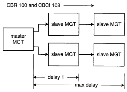
Figure 6 is a schematic block diagram of one of a plurality
of channel bonding configurations in accordance with the
present invention. In this illustration the slaves are
daisy chain coupled to the master. The master provides the
channel bonding request (CBR) 100 and the channel bonding
2o configuration information (CBCI) 108 to the first slave in
the chain. Delay 1 corresponds to the time it takes for
the first slave to have its channel bonding address
completely generated.
The first slave provides the CBR 100 and CBCI 108 to the
2~ second slave, which, in turn, provides the CBR and CBCI to
the third slave and so on. In this illustration, there are
four slaves coupled to the master. Thus, the time it takes
the fourth slave to completely generate its channel bonding
start address is the maximum delay, which is used by the
3o master and the other slaves to determine the channel
bonding commencement.
Figure 7 is a schematic block diagram of another one of the
plurality of channel bonding configurations in accordance
with the present invention. In this example, the master is
35 coupled to two slaves, which are each coupled to another
slave. In this illustration, the maximum delay is less
than in the example of Figure 6, since there are fewer
slaves in series. Note that the channel bonding
configuration information 108 is uniquely generated for
4o each channel bonding configuration.
16
CA 02538345 2006-03-08
WO 2005/027448 PCT/US2004/029867
As one of average skill in the art will appreciate, there
are numerous ways in which the master may be coupled to the
slaves for channel bonding. Further, by accounting for the
processing and propagation delays of the transceivers, any
number of transceivers may be bonded together without
encounter the latency issues of the past.
Figure 8 is a schematic block diagram of a channel bonding
module 90 operably coupled to the elastic storage buffer
88. In this embodiment, the channel bonding module 90
1o includes a pointer generation module 120, a channel bonding
sequence comparator 122, a channel bonding processing
module 124, and a clock correction module 126. In general,
the function of the channel bonding module 90, whether in
slave mode or master mode, is to read data from and write
data to its corresponding buffer at the same time and with
the same byte positioning as every other channel bonding
module 90 in a channel bond. Each of the modules of the
channel bonding module 90 may be separate processing
devices or contained in one processing device with multiple
2o functions. The processing module may have an associated
memory to store the corresponding operational instructions
of the functions performed by the processing device. Such
a processing device includes, but is not limited to,
microprocessor, micro-controller, digital signal processor,
microcomputer, central processing unit, field programmable
gate array, programmable logic device, state machine, logic
circuitry, analog circuitry, digital circuitry, and/or any
device that manipulates signals (analog and/or digital)
based on operational instructions.
3o In the example of Figure 8, which corresponds to the
example of Figure 4, the byte positioning of the data is
shifted by one byte. Thus, a single data block 130 or 132
is stored on two data word lines 128 of the buffer 88. For
instance, byte DO is stored at byte position B1 of a
particular data word line 128 of the buffer 88; byte D1 is
stored at byte position B2 of the same data word line; and
byte D2 is stored at byte position B3 of the same data word
line. Byte D4 of the data is stored at byte position BO of
a subsequent data word line of buffer 88. However, the
4o data block 130 is written to the buffer as if its stored in
17
CA 02538345 2006-03-08
WO 2005/027448 PCT/US2004/029867
the same data word line. Similarly, the data block 132 is
read from the memory as if it is stored on one data word
line. The channel bonding module 90 provides the memory
manipulation to accommodate the reading from and writing to
of data in this manner.
The channel bonding sequence comparator 122 compares bytes
of data as it is written into the buffer 88 with a channel
bonding sequence. When four bytes, regardless of their
byte position in the buffer 88, correspond to the channel
so bonding sequence, the channel bonding sequence comparator
122 generates a channel bonding sequence detect signal 134.
This is done in the same manner whether the channel bonding
module is in the slave mode or in the master mode.
In the master mode, the channel bonding processing module
124, generates a channel bonding sequence (CBS) address 136
based on the CBS_detect signal 134 and the write pointer
(write ptr). Typically, whatever address the write pointer
is pointing to at the time the CBS_detect signal 134 is
activated will be the CBS address 136. The channel bonding
2o processing module 124 also generates the channel bonding
request (CBR.) 100 and the channel bonding configuration
information (CBCI) 108 in response to the CBS.
The channel bonding processing module 124 generates the
CBCI 108 to include a number of slave transceivers,
propagation delays of each of the slave transceivers with
respect to the master transceiver transmitting the channel
bonding request, and clock correction information. The
channel bonding processing module 124 generates the clock
correction information by generating pointer separation
3o information (i.e., the difference between its read pointer
and its write pointer), generating an address offset (i.e.,
its byte positioning of when the first byte of the channel
bonding sequence), and generating an adjust enable signal.
The channel bonding processing module 124 also generates
its channel bonding start address 138 and its channel
bonding start indication 140 as was discussed with
reference to Figures 4 and 5. The pointer module 120
generates the read and write pointers for accessing the
buffer 88 in accordance with the start address 138.
18
CA 02538345 2006-03-08
WO 2005/027448 PCT/US2004/029867
In the master mode, the clock correction module 126 is
idle. In the slave mode, the clock correction module 126
generates pointer adjust information 142 based on the
channel bonding configuration information 108 (in
particular, the pointer separation, the address offset, and
may further include processing rate of the master), the
write pointer and the read pointer. Based on the pointer
adjust information 142 and in accordance with the adjust
enable signal, the pointer generation module 120 adjusts
1o the read pointer and write pointer to be byte aligned and
synchronous with the read and write pointers of the master,
even through they may be pointing to different addresses.
In other words, the pointer adjust information 142 enables
the pointer generation module 120 to insure that the read
and write pointers of a slave have the same address offset
and pointer separation as the master and that these
parameters are maintained.
In the slave mode, the channel bonding processing module
124 generates the channel bonding start address 136 and the
2o channel bonding start indication 140 based on the CBS
detect signal 134, the CBR 100, the CBCI 108, and the write
pointer. In this mode, the channel bonding processing
module 124 receives the CBR 100 and the CBCI 108 from the
master or another slave.
Another embodiment of the channel bonding module 90
includes a processing module and memory. The processing
module may be a single processing device or a plurality of
processing devices. Such a processing device may be a
microprocessor, micro-controller, digital signal processor,
3o microcomputer, central processing unit, field programmable
gate array, programmable logic device, state machine, logic
circuitry, analog circuitry, digital circuitry, and/or any
device that manipulates signals (analog and/or digital)
based on operational instructions. The memory may be a
single memory device or a plurality of memory devices.
Such a memory device may be a read-only memory, random
access memory, volatile memory, non-volatile memory, static
memory, dynamic memory, flash memory, cache memory, and/or
any device that stores digital information. Note that when
the processing module implements one or more of its
19
CA 02538345 2006-03-08
WO 2005/027448 PCT/US2004/029867
functions via a state machine, analog circuitry, digital
circuitry, and/or logic circuitry, the memory storing the
corresponding operational instructions may be embedded
within, or external to, the circuitry comprising the state
machine, analog circuitry, digital circuitry, and/or logic
circuitry. The memory stores, and the processing module
executes, operational instructions corresponding to at
least some of the steps and/or functions illustrated in
Figures 9 - 11.
1o Figure 9 is a logic diagram of a method for channel bonding
a plurality of multi-gigabit transceivers that begins at
step 150 where the master transceiver of the plurality of
mufti-gigabit transceivers receives a channel bonding
sequence. In one embodiment, the channel bonding sequence
i5 is received within incoming data and subsequently detected.
The process then proceeds to step 152 where the master
transceiver generates a channel bonding request in response
to the channel bonding sequence. The process then proceeds
to step 154 where the master transceiver transmits the
2o channel bonding request and channel bonding configuration
information to the slave transceivers.
The channel bonding configuration information includes a
number of slave transceivers, propagation delays of each of
the slave transceivers with respect to the master
25 transceiver transmitting the channel bonding request, and
clock correction information. The clock correction
information includes pointer separation information, an
address offset, and an adjust enable signal. The pointer
separation may be generated by determining a read pointer
30 of the master transceiver when the channel bonding sequence
is received to produce a master read pointer, determining a
write pointer of the master transceiver when the channel
bonding sequence is received to produce a master write
pointer, and determining the pointer separation as a
35 difference between the master read pointer and the master
write pointer. The address offset may be generated by
determining byte positioning of the channel bonding
sequence with respect to a word line of memory of the
master transceiver, and establishing the address offset
4o based on the byte positioning.
CA 02538345 2006-03-08
WO 2005/027448 PCT/US2004/029867
The process then proceeds to step 156 where each of the
slave transceivers receives the channel bonding sequence,
which may be contained within incoming data. The process
then proceeds to step 158 where each of the slave
transceivers receives the channel bonding request and the
channel bonding configuration information. The process
then proceeds to step 160 where each of the slave
transceivers processes the channel bonding request and the
channel bonding sequence in accordance with the channel
1o bonding configuration information to determine individual
slave channel bonding start information. The processing of
step 160 will be described in greater detail with reference
to Figure 10.
The processing of Figure 9 continues at step 162 where the
master transceiver processes the channel bonding sequence
in accordance with the channel bonding configuration
information and the channel bonding request to determine
master channel bonding start information. In one
embodiment this may be done by storing an address at which
2o the channel bonding sequence was received to produce a
channel bonding sequence address, and determining a channel
bonding write start address based on the channel bonding
sequence address and maximum propagation delay of the
channel bonding configuration information.
The process then proceeds to 'step 164 where channel bond
writing of respective data to and reading of the respective
data from corresponding buffers by the master transceiver
and the slave transceivers commences in accordance with the
individual slave channel bonding start information and the
3o master channel bonding start information.
Figure 10 is a logic diagram of the slave processing at
step 160 of the logic diagram of Figure 9. The processing
begins at step 170 where the channel bonding sequence is
delayed for a predetermined period of time based on the
propagation delays of a corresponding one of the slave
transceivers to produce a delayed channel bonding sequence.
The process then proceeds to step 172 where a determination
is made as to whether receipt of the channel bonding
request and the delayed channel bonding sequence are within
4o a time window. Such a determination may be made by
21
CA 02538345 2006-03-08
WO 2005/027448 PCT/US2004/029867
initiating the time window when one of the delay channel
bonding sequence or the channel bonding request is
received, and determining whether the other one of the
delay channel bonding sequence or the channel bonding
request is received prior to expiration of the time window.
The process then proceeds to step 174, where the process
branches to step 178 when the receipt of the channel
bonding request and the delayed channel bonding sequence
are within the time window and to step 176 when they
are
Zo not. At step 176, a channel bonding error is generated.
At step 178, a unique hold time is determined based
on a
difference between the propagation delay of the
corresponding one of the slave transceivers and a maximum
propagation delay. The process then proceeds to step
180
where an address at which the channel bonding sequ ence
was
received by the corresponding one of the slave transceivers
is stored to produce a channel bonding sequence address.
The process then proceeds to step 182 where a channel
bonding write start address is determined based on at least
one of: the channel bonding sequence address, the channel
bonding request, and the unique hold time. The process,
then proceeds to step 184 where a read pointer and a write
pointer of the corresponding one of the slave tran sceivers
are adjusted based on the pointer separation, the address
offset, and the channel bonding write start address.
Figure 11 is a logic diagram of a method for channel
bonding by a multi-gigabit transceiver that begins at step
190 where a determination is made as to whether the
multi-
gigabit transceiver is a master transceiver or a slave
3o transceiver. When the multi-gigabit transceiver is the
slave transceiver to process proceeds to step 190 where
a
channel bonding sequence is detected at a given time
to
produce a detected channel bond sequence. The process
then
proceeds to step 192 where the detected channel bonding
sequence is delayed for a predetermined period of time
to
produce a delayed channel bonding sequence. The process
then proceeds to step 194 where a channel bonding request
is received at a second given time.
The process then proceeds to steps 196 and 198 where
a
4o determination is made as to whether the receiving
of
22
CA 02538345 2006-03-08
WO 2005/027448 PCT/US2004/029867
channel bonding request and the delayed channel bonding
sequence are within a time window. This may be done by
first determining whether the delayed channel bonding
sequence occurs, in time, before the receiving of the
channel bonding request. ~nrhen the delayed channel bonding
sequence occurs before the receiving of the channel bonding
request, the determination continues by initiating a first
clock cycle count from the delay channel bonding sequence
to establish the time window and determining whether the
1o channel bonding request is received before expiration of
the first clock cycle count. When the channel bonding
request is received before expiration of the first clock
cycle count, the determination continues by determining
that the receiving of channel bonding request and the
delayed channel bonding sequence are within the time
window. ~h.en the delayed channel bonding sequence occurs
after the receiving of the channel bonding request, the
determination continues by initiating a second clock cycle
count from the receiving of the channel bonding request to
2o establish the time window, and determining whether the
delayed channel bonding sequence occurs before expiration
of the second clock cycle count. When the delayed channel
bonding sequence occurs before expiration of the second
clock cycle count, the determination continues by
determining that the receiving of channel bonding request
and the delayed channel bonding sequence are within the
time window. Tn~hen the delayed channel bonding sequence
occurs at substantially the same time as the receiving of
the channel bonding request, the determination continues by
3o determining that the receiving of channel bonding request
and the delayed channel bonding sequence are within the
time window.
If the channel bonding request and the delayed channel
bonding sequence are not within the time window as
determined in step 198, the process proceeds to step 200
where a channel bonding error is generate. If the
receiving of channel bonding request and the delayed
channel bonding sequence are within the time window, the
process proceeds to step 202 where data is aligned with
4o respect to data alignment of the master transceiver to
23
CA 02538345 2006-03-08
WO 2005/027448 PCT/US2004/029867
produce aligned data. The process the proceeds to step 204
where the aligned data is synchronized with data of the
master transceiver.
If the transceiver is a master, the process proceeds to
step 206 where the predetermined period of time is
established based on propagation delay between the master
transceiver detecting the channel bonding sequence and the
slave transceiver receiving the channel bonding request.
The process then proceeds to step 208 where an address at
1o which the channel bonding sequence was received is stored
to produce a channel bonding sequence address. The process
then proceeds to step 210 where a channel bonding write
start address is determined based on the channel bonding
sequence address and maximum propagation delay of channel
bonding configuration information.
As one of average skill in the art will appreciate, the
term "substantially", as may be used herein, provides an
industry-accepted tolerance to its corresponding term.
Such an industry-accepted tolerance may range, for example,
2o from less than one percent to twenty percent and may
correspond to, but is not limited to, component values,
integrated circuit process variations, temperature
variations, rise and fall times, and/or thermal noise. As
one of average skill in the art will further appreciate,
the term °operably coupled", as may be used herein,
includes direct coupling and indirect coupling via another
component, element, circuit, or module where, for indirect
coupling, the intervening component, element, circuit, or
module does not modify the information of a signal but may
3o adjust its current level, voltage level, andlor power
level. As one of average skill in the art will also
appreciate, inferred coupling (i.e., where one element is
coupled to another element by inference) includes direct
and indirect coupling between two elements in the same
3s manner as °operably coupled".
The preceding discussion has present a variety of
embodiments for channel bonding a plurality of multi-
gigabit transceivers. Such channel bonding is applicable
to any integrated circuit that includes a plurality of
4o high-speed interfaces and may be used with data word lines
24
CA 02538345 2006-03-08
WO 2005/027448 PCT/US2004/029867
of more or less than four bytes. As one of average skill
in the art will appreciate, other embodiments may be
derived. from the teachings of the present invention without
deviating from the scope of the Claims.