Note: Descriptions are shown in the official language in which they were submitted.
CA 02538851 2006-03-08
Attorney Docket OS-1-285
METHOD OF SETTING DESIRED RMS LOAD VOLTAGE IN A LAMP
Background of the Invention
[0001] The present invention is directed to a power controller that supplies a
specified power to a load, and more particularly to a lamp with a voltage
converter that
converts line voltage to a voltage suitable for lamp operation.
[0002] Some lamps operate at a voltage lower than a line (or mains) voltage
of,
for example, 120V or 220V, and for such lamps a voltage converter that
converts line
voltage to a lower operating voltage must be provided. A lower lamp operating
voltage
provides benefits, including the ability to use a filament wire with a larger
cross section
and shorter length, thereby increasing lamp efficiency, color temperature and
filament
efficacy, and improving sag resistance, hot shock resistance and vibration
induced
flickering.
[0003] Power supplied to a lamp may be controlled with a phase-control clippW
g
circuit that typically includes an RC circuit and uses phase-control clipping
to reduce the
line voltage to an RMS load voltage suitable for operation of the light
emitting element of
the lamp.
[0004] A simple four-component RC phase-control clipping circuit is shown in
Figure 1 and includes a capacitor 22, a diac 24, a triac 26 that is triggered
by the diac 24,
and resistor 28. The resistor 28 may be a potentiometer that sets a resistance
in the circuit
CA 02538851 2006-03-08
to control a phase at which the triac 26 fires. The RMS load voltage and
current are
determined by the resistance and capacitance values in the clipping circuit
since the phase
at which the clipping occurs is determined by the RC series network and since
the RMS
voltage and current depend on how much energy is removed by the clipping.
Figure 2
illustrates a clipped waveform formed by a phase-control clipping circuit such
as
illustrated in Figure 1.
[0005] The phase-control clipping circuit has drawbacks. As seen in Figure 2,
the
voltage is applied to the lamp light emitting element (e.g., filament) part
way through the
power cycle. This causes a current pulse that can generate electromagnetic
interference
(EMI) and cause harmonic distortion (THD). Filtering elements (e.g., chokes)
may be
installed to reduce EMI and THD but such elements can increase the cost,
weight and
size of the system and can generate heat.
[0006] Another drawback of the phase-control clipping circuit is that the lamp
may not operate properly when driven by a dimmer that delivers a clipped line
voltage
waveform to the lamp. The phase-control clipping circuit shown in Figure 1
needs a sine
wave voltage input for the phase setting components to operate correctly. If
the line
voltage has been clipped by a dimming circuit so that a sinusoidal voltage
waveform is
no longer presented to the lamp, the phase-control clipping circuit may not
trigger the
diac and triac as intended.
[0007] Further, it is desirable to provide a filament for a lamp that is
designed for
a particular operating voltage. However, variations in line voltage cause the
operating
voltage to vary (for example, by as much as 10%) and thus filament have been
designed
2
CA 02538851 2006-03-08
to operate over a range of voltages, which may include voltages that cause the
filament to
operate with less than the desired effect.
[0008] When the phase-control power controller is used in a voltage converter
of
a lamp, the voltage converter may be provided in a fixture to which the lamp
is connected
or within the lamp itself. U.S. Patent 3,869,631 is an example of the latter,
in which a
diode is provided in an extended stem between the lamp screw base and stem
press of the
lamp for clipping the line voltage to reduce RMS load voltage at the light
emitting
element. U.S. Patent 6,445,133 is another example of the latter, in which a
voltage
conversion circuit for reducing the load voltage at the light emitting element
is divided
with a high temperature-tolerant part in the lamp base and a high temperature-
intolerant
part in a lower temperature part of the lamp spaced from the high temperature-
tolerant
part.
Summary of the Invention
[0009] An object of the present invention is to provide a novel lamp and
method
in which an internal voltage controller converts a line voltage to a desired
RMS load
voltage using pulse width modulation (PWM).
[0010] A further object is to provide a novel lamp with a voltage controller
that is
entirely within a lamp base and uses PWM to define an RMS load voltage, where
the
voltage controller includes a feed-back circuit that adjusts the RMS load
voltage to a
desired level based on a comparison of the load voltage to a preset reference,
and a
switching transistor that pulse width modulates lamp current and that is
responsive to the
CA 02538851 2006-03-08
feed-back circuit to adjust the duty cycle of the switching transistor to
cause the RMS
load voltage to reach the desired level.
[0011] A yet further object is to provide a novel lamp and method in which an
internal voltage controller converts a line voltage to a predetermined RMS
load voltage
using a microcontroller that compares the RMS load voltage to a reference and
adjusts
the duty cycle of the switching transistor based on a result of the
comparison.
Brief Description of the Drawings
[0012] Figure 1 is a schematic circuit diagram of a phase-controlled clipping
circuit of the prior art.
[0013] Figure 2 is a graph illustrating voltage clipping in the phase-
controlled
clipping circuit of Figure 1.
[0014] Figure 3 is a partial cross section of an embodiment of a lamp of the
present invention.
[0015] Figure 4 is a schematic circuit diagram showing an embodiment of the
present invention.
[0016] Figure S is a graph depicting the pulse width modulation of the load
voltage of the present invention.
[0017] Figure 6 is a circuit diagram of a further embodiment of the present
invention.
4
CA 02538851 2006-03-08
Description of Preferred Embodiments
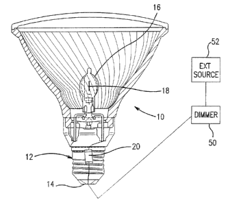
[0018] With reference to Figure 3, a lamp 10 includes a base 12 that is
arranged
and adapted to fit into a lamp socket and has an exterior lamp terminal 14
that is adapted
to be connected to line voltage, a light-transmitting envelope 16 attached to
the base 12
and housing a light emitting element 18 (an incandescent filament in the
embodiment of
Figure 3), and a lamp internal voltage conversion circuit 20 for converting a
line voltage
at the lamp terminal 14 to a desired RMS load voltage.
[0019] The voltage conversion circuit 20 is housed entirely within the base 12
(that is, entirely within the part of the lamp that is arranged and adapted to
fit into a lamp
socket such as shown in Figure 3) and connected in series between the lamp
terminal 14
and the light emitting element 18. The voltage conversion circuit 20 may be an
integrated circuit in a suitable package as shown schematically in Figure 3.
[0020] While Figure 3 shows the voltage conversion circuit 20 in a parabolic
aluminized reflector (PAR) halogen lamp, the voltage conversion circuit 20 may
be used
in any incandescent lamp when placed in series between the light emitting
element (e.g.,
filament) and a connection to a line voltage (e.g., lamp terminal).
(0021] With reference to Figure 4 that illustrates an embodiment of the
present
invention, the voltage conversion circuit 20 includes line terminals 32 for a
line voltage
and load terminals 34 for a load voltage, and a PWM circuit 36 that pulse
width
modulates the load voltage and that is connected to the line and load
terminals. The
PWM circuit 36 includes a transistor switch 38 that pulse width modulates the
current
supplied to a bridge 40 that provides the RMS load voltage to the lamp, and a
microcontroller 42. The microcontroller 42 includes a time-based signal source
that
CA 02538851 2006-03-08
sends time-based signals to a gate of the transistor switch 38 and a feed-back
circuit that
compares the load voltage to a reference and adjusts a duty cycle of the
transistor switch
38 (ON time compared to total time) based on the comparison so that the RMS
load
voltage reaches the desired level. The duty cycle (set by changing frequency
and/or
duration of the time-based signals) determines the total time per cycle that
the transistor
switch is ON, which defines the RMS load voltage.
[0022] In one embodiment, microcontroller 42 includes an analog-to-digital
converter (ADC) that converts the load voltage to a digital value, a
comparator that
compares the output from the ADC to a preset reference value, and a program
(e.g., in a
hardwired and/or programmable circuit) that adjusts the duty cycle of the
transistor
switch (e.g., increasing the duration of the pulses to increase the RMS load
voltage)
based on an output from the comparator so that the desired RMS load voltage is
reached.
The reference value is preset to a value that provides the desired RMS load
voltage for
the lamp. The structure and operation of microcontroller 42 need not be
described in
detail as such microcontrollers are known in the art and are commercially
available from
various sources, including Microchip Technology, Inc. under the PIC trademark
(e.g., a
PICTM 8-pin 8-bit CMOS microcontroller, such as PIC12F683).
[0023] In operation, the microcontroller 42 generates signals (e.g., pulses)
whose
frequency and duration provide a transistor switch duty cycle that is
appropriate for the
desired RMS load voltage. The signals are applied to the gate of the
transistor switch so
that the voltage applied to the light emitting element is switched ON and OFF
at much
greater speed than the line voltage frequency (typically 50-60 Hz). The
frequency of the
signals is desirably higher than the audible range (i.e., above about 20 kHz).
Figure 5
CA 02538851 2006-03-08
shows an example of an incoming voltage waveform and a pulse width modulated
voltage waveform (the frequency being reduced to illustrate the modulation).
[0024] The microcontroller senses the load voltage and compares this voltage
to a
reference that has been set in advance to provide the desired RMS load
voltage. The
microcontroller then adjusts the RMS load voltage to the desired amount by
adjusting the
triggering of conduction in PWM circuit 36 based on the comparison.
[0025] In an alternative embodiment, the feed-back circuit includes separate
components (e.g., timer, comparator, timer adjustment program) that perform
the above-
described functions, rather than a microcontroller.
[0026] With reference now to Figure 6, a particular embodiment of the present
invention includes a full-wave bridge 44, an insulated gate bipolar transistor
46 (which
alternatively may be a MOSFET), and a programmable microcontroller 48 (e.g., a
PICTM
microcontroller) that includes an analog-to-digital converter. The
microcontroller 48
monitors the voltage on the output line and automatically adjusts the duty
cycle of the
pulse stream delivered to the transistor switch such that the RMS load voltage
supplied to
the lamp filament is constantly at the desired level. Inputs to the
microcontroller 48 may
be provided by including appropriate circuitry such as the connections,
resistors and
capacitors in Figure 6, which are shown by way of example. The microcontroller
desirably is or operated to be astable (not having a stable state at which it
can rest). A
heat sink (not shown) may be attached to the transistor switch as needed.
[0027] With reference again to Figure 3, the lamp may also include a dimmer 50
that clips a line voltage. The dimmer 50 is external to the lamp I O and
connected
between exterior lamp terminal 14 and an external source of the line voltage
52. The
CA 02538851 2006-03-08
dimmer may be a conventional forward or reverse phase-control dimmer, or pulse
width
modulation dimmer, that delivers a clipped line voltage waveform (such as the
forward
clipped waveform shown in Figure 2) to the line terminals of the lamp. The PWM
voltage controller of the present invention operates independently of line
voltage
magnitude and waveform and thus is not affected by the clipping.
[0028] Since the voltage conversion circuit is not divided into separate
parts, such
as the high temperature tolerant and intolerant parts in the above-cited U.S.
Patent
6,445,133, the cost for the circuit is reduced and manufacturing complexity is
reduced.
Further, since the voltage conversion circuit is not in the stem and the size
of the stem is
not affected by the addition of the circuit within the lamp (see the extended
stem in the
above-cited U.S. Patent 3,869,631), the complexity of the stem and the
manufacturing
cost thereof and the size of the lamp are reduced.
[0029] The addition of the PWM voltage controller inside the lamp base as an
integral component of the lamp, rather than separately external to the lamp,
permits the
use of optimized low-voltage filaments in lamps intended for use with standard
sockets,
thereby improving lamp beam performance, color temperature, efficacy, sag
resistance,
hot shock resistance, and vibration-induced flickering resistance.
[0030] While conventional RC phase-control clipping circuits are very
sensitive
to fluctuations in the line voltage magnitude, the present invention provides
a power
controller that operates substantially independently of the incoming line
voltage
magnitude and waveform because no component of the PWM voltage controller is
dependant on the magnitude or waveform of the incoming signal. Additionally,
because
the current is drawn from the incoming signal equally during all periods of
the input
CA 02538851 2006-03-08
cycle, PWM of load voltage avoids the phase-control clipping pulses that cause
EMI and
THD in the prior art. This advantage is particularly significant when a large
number of
lamps are connected to the same supply circuit.
[0031] The present invention affords the additional advantage that the lamp
filament can be designed specifically for a predetermined reduced voltage. By
operation
of the present invention, the lamp designer is assured that the filament will
receive this
predetermined voltage.
[0032] While embodiments of the present invention have been described in the
foregoing specification and drawings, it is to be understood that the present
invention is
defined by the following claims when read in light of the specification and
drawings.