Note: Descriptions are shown in the official language in which they were submitted.
CA 02538965 2001-03-02
WAVELENGTH COMPENSATED OPTICAL WAVELENGTH DIVISION COUPLER AND
ASSOCIATED METHODS
BACKGROUND OF THE INVENTION
Field of the Invention
The present invention is directed to a wavelength compensated optical
wavelength
division coupler, more particularly to an integrated coupler.
Description of Related Art
to Optical multiplexers/demultiplexers are generally known in the art. See,
for example,
U.S. Patent No. 4,244,045 entitled "Optical Multiplexer and Demultiplexer",
which is hereby
incorporated by reference in its entirety for all purposes. In the
configurations set forth therein,
the mux/demux includes a plurality of filters for the respective wavelengths,
a corresponding
plurality of prisms for providing the filtered light from/to a corresponding
plurality of
t s sources/detectors and a corresponding plurality of elements for
collimating/condensing light. The
multiplex path that either receives or supplies the multiplexed light includes
a prism and an
element for condensing/collimating light.
As can be seen in the '045 patent, a plurality of narrow band pass filters are
required, one
for each of the channels. To multiplex a plurality of channels requires a
plurality of narrow band
2o pass (NBP) filters connected in series such that the output of one filter
provides part of the input
to another. This serial connection typically requires a critical off-axis
alignment that must be
precisely controlled. As shown in the '045 patent, this involves introducing a
light beam at a
desired incident angle using the lens and the prism. Since each of the
multiple beams required a
different incident angle, different prisms are used for each beam. These
prisms are very small,
25 making them difficult to manufacture and making further reduction in size
of the multiplexer
impractical. Another example of such adjustment includes fixing the NBP
filters and then
adjusting the location of the ports for the input and output of light to
thereby control the angle of
incidence on the filter. Since each beam requires different angles, and thus
different prisms, in
using these configurations for multiple beams, very small different prisms are
required.
3o Attention has been focused on eliminating these small parts and separate
filters. One
solution involves using linear variable filters, as set forth in U.S. Patent
5,583,683 entitled
"Optical Multiplexing Device" to Scobey. The device disclosed therein is a
parallel optical block
having a filter of varying thickness on at least one side thereof. The light
is incident on the block
at the same tilt angle, but due to the varying thickness of the filter,
different wavelengths are
3s transmitted at each port, with the remaining wavelengths being reflected,
again creating the
CA 02538965 2001-03-02
zigzag pattern of the '045 patent. However, thickness control is difficult to
reliably achieve and
the control of the input tilt angle is also critical. Another solution
involves using a wedge-shaped
optical block with the filter on at least one side thereof. The wedged shaped
optical block used
therein results in the sequentially reflected light beams striking the
wavelength selective filter at
different angles.
However, even these integral filter element solutions still require precise
control of either
filter thickness or wedge profile. Further, the number of channels to be
practically multiplexed by
the variable filter thickness is limited by process control and to be
practically multiplexed by the
wedge shaped due to the increased length needed to accommodate many channels.
Therefore,
t o while these configurations may overcome some of the attendant problems of
numerous separate
filters, they still require expensive angular alignments.
SUMMARY OF THE PRESENT INVENTION
The present invention is therefore directed to an integrated coupler that
substantially
overcomes one or more of the problems due to the limitations and disadvantages
of the related
art.
It is an object of the present invention to create a multiplexer having fewer
individual
parts, thereby improving manufacturability and scalability.
At least one of these and other objects may be realized by providing an
optical device
including a wavelength selective filter, a first port for propagating at least
a first wavelength, a
second port for propagating at least a second wavelength different from the
first wavelength, a
third port for propagating at least the first wavelength and the second
wavelength, and at least
two individual optical elements, each optical element being associated with
one of the ports,
between an associated port and the wavelength selective filter, wherein all
optical elements
needed for directing light between the ports and the wavelength selective
filter are provided on at
least one of a substrate and substrates bonded thereto. All three ports are
positioned relative to
the wavelength selective filter
The wavelength selective filter and the at least two optical elements may be
integrated on
a wafer level. The wavelength selective filter may be a multi-layer dielectric
stack formed on one
of the substrates. The bonding of substrates may occur at a wafer level, and
the bonded
substrates are diced to form the optical device. The at least two optical
elements may be formed
lithographically.
The at least two optical elements may be diffractive elements. The diffractive
elements
may have a same deflection grating. The at least two diffractive elements may
include at least
three diffractive elements. The diffractive elements may perform both
deflection and collimation.
2
CA 02538965 2001-03-02
The at least two optical elements may be refractive elements. The refractive
elements may be
off-axis refractive elements. The at least two optical elements may include a
pair of optical
elements. The pair of optical elements may include a refractive element and a
diffractive
element. All optical elements may be provided on a single substrate. The at
least two optical
elements may be provided on a same surface.
The optical device may include light sources adjacent to substrates on which
optics!
elements are formed. The optical device may include power monitors for the
light sources. The
at least two optical elements may deflect a portion of the light from each of
the light sources onto
a respective power monitor.
to At least one of the above and other objects may be realized by providing a
diffractive
multiple wavelength optical coupler including at least two diffractive
elements having a same
deflection grating period, each diffractive receiving a substantially
monochromatic light beam, a
wavelength selective filter for at least one of the at least two diffractive
elements, the wavelength
selective filter passing a desired wavelength and reflecting all other
wavelengths; and a multiplex
~ 5 diffractive receiving a multiplex optical signal. The coupler may serve as
a multiplexes or a
demultiplexer. The at least two diffractives may include at least three
diffractives, wherein a
spacing between adjacent diffractives is different from one another.
At least one of the above and other objects of the present invention may be
realized by
providing a multiple wavelength optical coupler including at least a first,
second and third surface
20 on which an optical function is performed, at least two individual optical
elements, each individual
optical element receiving a substantially monochromatic light beam, the at
least two individual
optical elements being formed on the first surtace, a wavelength selective
filter that passes a
desired wavelength and reflect all other wavelengths formed on a second
surface, the third
surface reflecting light incident thereon, and a multiplex optical element
receiving a multiplex
25 optical signal.
The coupler may serve as a multiplexes or as a demultiplexer. The individual
optical
elements may be refractive elements and/or diffractive elements. The at least
two individual
optical elements may include at least three individual optical elements,
wherein a spacing
between adjacent individual optical elements is different from one another.
3o At least one of the above and other objects may be realized by providing a
multiple
wavelength optical coupler including at least three separate optical elements,
each individual
optical element receiving a substantially monochromatic light beam, wherein
each separate
optical element outputs light at a different deflection angle and a spacing
between adjacent
individual optical elements is different from one another, a plurality of
wavelength selective filters,
35 a wavelength filter being provided for at least two of the three separate
optical elements, each
3
CA 02538965 2001-03-02
wavelength selective filter passing a desired wavelength and reflecting all
other wavelengths,
and a multiplex optical element receiving a multiplex optical signal. The
coupler may serve as a
multiplexer or as a demultiplexer. The separate optical elements may be
refractive elements
and/or diffractive elements.
s At least one of the above and other objects may be realized by providing a
method of
coupling multiple wavelengths including receiving a plurality of substantially
monochromatic light
beams at a corresponding plurality of ports, each port receiving a
monochromatic light beam of a
different wavelength, providing an optical element at each port, each optical
elements outputting
light at a particular deflection angle, wavelength selectively filtering at
each non-terminal port, the
~ o filtering including passing the substantially monochromatic light beam
associated with the port
and substantially reflecting all other wavelengths, directing the
substantially monochromatic light
beams between the optical elements and a multiplex port, and receiving a
multiplex optical signal
at a multiplex port. The providing may include, when there are at least three
optical elements,
spacing adjacent optical elements differently from one another. The optical
elements may output
is light at the same or different, unique deflection angles.
In an aspect of the invention, there is provided an optical component,
comprising a
mirror-filter block positioned with respect to the light beam so that light
entering the mirror-filter
block is wavelength separated through a plurality of reflections between a
flat mirror surface and
a plurality of filters coupled between the collimating lens and a lens array
and a plurality of
2o focusing lenses formed on the fens array, each of the plurality of focusing
lenses optically
coupled to one of the plurality of filters.
In another aspect, there is provided a method of demultiplexing a light beam,
comprising
collimating the light beam with a collimating lens, separating each wavelength
of light from the
light beam by reflecting the light beam between a flat mirror and a plurality
of optical filters, each
25 of the plurality of optical filters passing light in a narrow region about
a specified wavelength
propagating light passed through each of the plurality of optical filters
substantially along the
optical axis of one of a plurality of focusing lenses and focusing light from
each of the plurality of
optical filters with one of the plurality of focusing lenses.
These and other objects of the present invention will become more readily
apparent from
3o the detailed description given hereinafter. However, it should be
understood that the detailed
description and specific examples, while indicating the preferred embodiments
of the invention,
are given by way of illustration only, since various changes and modifications
within the spirit and
scope of the invention will become apparent to those skilled in the art from
this detailed
description.
4
CA 02538965 2001-03-02
BRIEF DESCRIPTION OF THE DRAWINGS
The foregoing and other objects, aspects and advantages will be described with
reference
to the drawings, in which:
Figure 1 is a schematic cross-sectional view of a multiplexer using different
single
wavelength channel diffractives;
Figure 2 is a schematic cross-sectional view of a multiplexer using the
identical s ingle
wavelength channel diffractives;
Figure 3A is an elevational perspective view of a plurality of fibers
integrated with a
multiplexer;
t o Figure 3B is an elevational exploded perspective view of a plurality of
fibers housed in v-
grooves;
Figure 4 is detailed schematic cross-section of a multiplexer of the present
invention;
Figure 5 is a perspective elevational view of the detailed schematic of Figure
4;
Figure 6 is a schematic side view of the paths taken by light of different
wavelengths
through the multiplexer;
Figure 7A is a schematic cross-section of a multiplexer of the present
invention using
refractive elements and diffractive elements; and
Figure 7B is a schematic cross-section of a multiplexer of the present
invention using off-
axis refractive elements.
DETAILED DESCRIPTION OF PREFERRED EMBODIMENTS
Since filters are readily available in sheets and other optical elements are
readily
produced on the wafer level, it is practical to provide the optical elements
on a separate surface
from the filters. While individual diffractive elements, off-axis refractive
elements, or combination
of diffractive and on-axis refractive elements could be provided or formed on
the filter itself, to
substitute for the prisms in the above related configurations, this often does
not result in the most
scaleable, manufacturable configuration. Further, reflective surfaces are
still needed to transfer
the light beams to/from the multiplexed signal. Therefore, it is often
convenient to provide at
least three surfaces on which the optical elements, including the reflector,
and the filters may be
3o provided. One method for forming more than two surfaces on which to provide
at least one
optical element is set forth, for example, in U.S. Patent No. 6,096,155, which
is hereby
incorporated by reference in its entirety for all purposes. As used herein,
"wafer level" is to mean
any production of multiple optical systems that are subsequently diced for
final use.
A diffractive optical multiple wavelength coupler 1 including two substrates
5, 25 is shown
3s in Figure 1. Only two separate light paths, each for a particular
wavelength of light, are shown for
5
CA 02538965 2001-03-02
simplicity. Further, while the following explanation assumes the device is
operating as a
multiplexer, the device could clearly also function as a demultiplexer. Light
of different
wavelengths is input to respective separate interfaces 10, 12 which direct the
light through a
substrate 5 to a corresponding individual diffractive 20, 22. Light 15a
passing through the
diffractive 20 is incident upon a wavelength filter 30, which allows only
light at a desired
wavelength to pass therethrough. If the light 15a is sufficiently
monochromatic for a desired end-
use, the wavelength sensitive filter 30 may be eliminated. Light passing
through the filter 30 and
the substrate 25 is internally reflected at an opposite surface 35 of the
substrate 25, either due to
total internal reflection or to a reflective coating provided on the opposite
surface. Light 15b
t o passing through the diffractive 22 is incident upon a wavelength filter
32. The light 15a reflected
from the opposite surface 35 is also incident on the wavelength filter 32.
Since the wavelength
filter 32 transmits the wavelength of light 15b and reflects all other
wavelengths, both light 15a
and 15b are directed back to the surface 35, where they are reflected to a
multiplex diffractive
40. This multiplex diffractive 40 directs the light 15a, 15b through the
substrate 5 onto a
t 5 multiplex interface 50, which, e.g., supplies the multiple wavelengths to
a single fiber.
In accordance with conventional design, such as in the prisms of the '045
patent, each of
the individual diffractives 20, 22 outputs light therefrom at the same angle.
Since diffractives are
highly wavelength dependent, this requires a different diffractive grating for
each wavelength.
However, upon reaching the multiplex diffractive 40, the light output
therefrom will not all be
2o collimated and focused on the multiplex interface 50, since the performance
of diffractives is
highly wavelength dependent. In other words, the light delivered at the same
angle to the
multiplex diffractive 40 will be output at different angles. Thus, a lot of
the light will be lost.
In accordance with an illustrative embodiment of the present invention, as
shown in
Figure 2, a diffractive optical multiple wavelength coupler 2 has individual
diffractives 24, 26
25 which all have the same grating period for deflection. Thus, the
combination of the individual
diffractives 24, 26 and the multiplex diffractive 40 will be independe nt of
wavelength. In other
words, since the individual diffractive 24, 2 will diffract each wavelength
differently, light at
different wavelengths will reach the multiplex diffractive 40 at different
angles. Thus, while light
15a will still be reflected by the opposite surface 35 and directed onto the
wavelength filter 32,
3o the light 15a and 15b from the wavelength filter 32 will be traveling at
different deflection angles.
Since fight 15a, 15b of different wavelengths will be incident on the
multiplex diffractive at
different angles, the multiplex diffractive 40 then will collimate all of the
different wavelengths and
output them to the multiplex interface 50.
Thus, in accordance with the present invention, each pair of diffractives,
i.e., an individual
35 diffractive 24, 26 and the multiplex diffractive 40, acts as an achromatic
pair. In other words, the
6
CA 02538965 2001-03-02
diffractives compensate for one another for differences in wavelengths.
Further, even if the
wavelength varies from a desired output, the diffractive pair will self-
compensate for this shift.
Each diffractive 24, 26 40 may be a deflection grating plus an on-axis lens.
When the
lens function is added to the diffractives 24, 26 while the deflection grating
remains the same for
all lenses, the lens function will be different, resulting in different
diffractive structures for the
different wavelengths. The lens portion for each diffractive is to be designed
for a different focal
length so that the multiplex lens 40 focuses the light to the same depth along
the z-axis.
Alternatively, the lens function of the diffractives 22, 26, 40 may be
replaced by a plurality of the
same refractive lenses. These refractive lenses are not nearly as wavelength
dependent, i.e.,
to have much less chromatic dispersion than diffractive lenses, so the same
refractives may be
used for the light 15a, 15b. If the refractives are to be positioned where the
diffractives are, the
diffractives supplying the deflection could be provided on the refractives or
on the filters.
The interfaces 10, 12, 50 illustrated in Figures 1 and 2 are shown as they
would appear if
they constituting an optical fiber butt-coupled to the interfaces, with the
light diverging therefrom.
Alternatively, associated lenses for collimating the light before the
interface may be provided,
which would result in the fibers being spaced from the interfaces. These
associated lenses
could be used for separate interfaces 10, 12 and/or multiplex interface 50.
Further, the actual
light sources may be provided without the use of a fiber or other delivery
structure.
When the light is deflected at different angles from the separate diffractives
24, 26, the
2o multiplex diffractive 40 will provide all the light to the multiplex
interface 50 at the correct angles,
but the position of these beams will be shifted from the center in the x-y
direction. One way of
compensating for this positional shift is to vary the spacing of the
individual lenses 22 and the
corresponding filters 30 across the array so that all the beams are incident
at the same cross-
sectional position on the lens 40. This also will result in varying the
position of the separate
interfaces 10, which may include varying the position of the corresponding
fibers in an array or
providing some deflection between a fiber array and the interfaces to have the
light thereon
properly positioned. Variation in fiber spacing is advantageously provided
using v-grooves 60
aligned with the coupler to hold fibers 70 therein, as shown in Figure 3a and
3b. V-grooves may
also obviously be used in conjunction with a regular array. The fibers in the
v-grooves may be
3o aligned with the coupler 2 using passive alignment techniques.
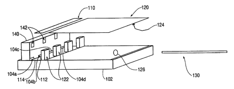
A detailed configuration for more than two beams is shown in Figure 4. Figure
4 is a
schematic cross-section of the multiplexes of the present invention. An array
104 of light
sources 104a-104d, here shown as vertical cavity surface emitting lasers
(VCSELs), is provided
on a substrate 102. Light output by the light source array 104 is directed to
a first optics block
110 having a corresponding plurality of collimating/deflecting elements 112.
The light source
CA 02538965 2001-03-02
array 104 is separated from the first optics block 110 by a spacer 106, here
shown as etched
silicon. The collimated/deflected light then hits a corresponding plurality of
filters 122, one for
each appropriate wavelength of light. The filters 122 are preferably mounted
on or formed on a
second optics block 120, but may be provided on a separate, intermediate
optics block.
The light passing through the filters 122 is directed to an opposite surface
of the optics
block 120 having a reflective element 124 thereon. In this particular
configuration, the opposite
side of the optics block 120 also has a focusing/deflecting element 126
thereon for focusing the
light onto a fiber 130, which, as shown in Figure 4, may be housed in an MT-RJ
connector 132.
The light reflected by the reflective element 124 is directed back toward the
input surface of the
to optics block 120 where it is incident on another filter of the plurality of
filters 122. Since each
filter will only pass light of a particular wavelength and the light source
array 104 has light
sources of different wavelengths, all of the filters other than the
corresponding filter at the output
of the light source will reflect the light back toward the other surface of
the optics block 120.
Each corresponding filter allows the light from the corresponding light source
to pass
therethrough to thereby enter the optics block 120.
A schematic perspective, elevational view of the multiplexer of Figure 4 is
shown in
Figure 5, along with an array of detectors 142 for monitoring the outputs of
the light sources. In
Figure 5, the light sources 104a-104d are edge emitting light sources, rather
than the vertical
emitting sources of Figure 4. For providing light to the detectors 142, the
first optics block 110
2o further includes a plurality of splitting/deflecting elements 114 for
splitting off a portion of the light
and directing it up and back towards the detectors 142. In this embodiment,
the reflective
surface 124 on the optics block 120 reflects the split light back to the
detectors 142. The rest of
the beam that is not split off continues to the collimatingldeflecting
elements 112 as in Figure 4.
These elements may be combined 112, 114 may be combined. In the particular
configuration
shown in Figure 5, the first and second optics blocks 110, 120 are mounted on
the same
substrate 102 as the light sources 104a-104d, which here are edge-emitting
lasers.
Figure 6 illustrates a side view of the path light will take through the
multiplexer. As can
be seen therein, light from an edged emitting light source incident at a first
port 150 is collimated
and deflected. No filter is required at this end of the system, since the
wavelength corresponding
3o to the first port is the only wavelength either remaining in or input to
the system. Light 151'
incident at a second port 151 is also collimated and deflected at a different
angle as the light
input at the first port. The light 151' is also incident on a filter that
transmits light 151' while
reflecting light 150'. Similarly, light 152' and 153' incident at third and
fourth port 152, 153
respectively, is collimated and deflected at a different angle as the light
input at the first and
second ports, and from each other. The light 152' is also incident on a filter
that transmits light
8
CA 02538965 2001-03-02
152' while reflecting light 150', 151', while light 153' is incident on a
filter that transmits light 153'
while reflecting light 150', 151', 152'. Finally, element focuses multiplexed
light 154' to a
multiplex port 154.
Figures 7A and 7B illustrate refractive embodiments of the present invention.
Figure 7A
illustrates a multiplexer using refractive elements 160 for each of the ports.
In this configuration,
the diffractive elements 24, 26 are the same and serve to provide the
deflection angle, which will
then be different for the different wavelengths form the light sources 104a,
104b. Otherwise the
operation is the same as in Figure 2. This configuration provides the
efficiency of refractive
elements for focusing and collimating the beam, while using the difference in
deflection angles
to output from the diffractive elements to reduce the requirements on the
wavelength filters.
Figure 7B is an all refractive configuration in which off-axis refractive
elements 170 are
used to provide the deflection angle as well as the collimating and focusing.
The light at different
wavelengths from 104a, 104b output from these off-axis refractives 170 will
have the same
angle, so the requirements on the wavelength filter 32 are not reduced.
However, this
t 5 configuration is the most efficient regarding the optical power.
Thus, the present invention results in an integrated wavelength compensated
coupler
that may include a power monitor for the light sources. While the above
embodiments have
described regarding a multiplexer, it is to be understood that the active
elements may instead be
detectors, with the multiplex port 154 serving as the input port and first-
fourth ports serving as
20 output ports. Further, the wavelength filter at the terminal end is
optional.
While the present invention is described herein with reference to illustrative
embodiments
for particular applications, it should be understood that the present
invention is not limited
thereto. Those having ordinary skill in the art and access to the teachings
provided herein will
recognize additional modifications, applications, and embodiments within the
scope thereof and
25 additional fields in which the invention would be of significant utility
without undue
experimentation. Thus, the scope of the invention should be determined by the
appended
claims and their legal equivalents, rather than by the examples given.
35
9